EP0375900A2 - Système ordinateur - Google Patents
Système ordinateur Download PDFInfo
- Publication number
- EP0375900A2 EP0375900A2 EP89120836A EP89120836A EP0375900A2 EP 0375900 A2 EP0375900 A2 EP 0375900A2 EP 89120836 A EP89120836 A EP 89120836A EP 89120836 A EP89120836 A EP 89120836A EP 0375900 A2 EP0375900 A2 EP 0375900A2
- Authority
- EP
- European Patent Office
- Prior art keywords
- message
- bus
- iocp
- messages
- control means
- Prior art date
- Legal status (The legal status is an assumption and is not a legal conclusion. Google has not performed a legal analysis and makes no representation as to the accuracy of the status listed.)
- Withdrawn
Links
Images


Classifications
-
- G—PHYSICS
- G06—COMPUTING; CALCULATING OR COUNTING
- G06F—ELECTRIC DIGITAL DATA PROCESSING
- G06F13/00—Interconnection of, or transfer of information or other signals between, memories, input/output devices or central processing units
- G06F13/10—Program control for peripheral devices
- G06F13/12—Program control for peripheral devices using hardware independent of the central processor, e.g. channel or peripheral processor
- G06F13/122—Program control for peripheral devices using hardware independent of the central processor, e.g. channel or peripheral processor where hardware performs an I/O function other than control of data transfer
-
- G—PHYSICS
- G06—COMPUTING; CALCULATING OR COUNTING
- G06F—ELECTRIC DIGITAL DATA PROCESSING
- G06F13/00—Interconnection of, or transfer of information or other signals between, memories, input/output devices or central processing units
- G06F13/14—Handling requests for interconnection or transfer
- G06F13/36—Handling requests for interconnection or transfer for access to common bus or bus system
- G06F13/362—Handling requests for interconnection or transfer for access to common bus or bus system with centralised access control
Definitions
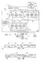
- the IOCP 38 is attached to the CPU by way of a communication bus 44.
- This bus allows either processor (CPU or IOCP) to transfer interrupt and control information to the other.
- the IOCP is attached to the IOPs via a bus 39.
- the IOPs are intelligent microprocessor-based subsystems providing control of attached I/O devices. It is contemplated that the designer might provide multiple IOP subsystems, with each specific type of IOP dedicated to a particular category of I/O devices. Varying system I/O requirements would lead to different combinations of IOPs. It is further comtemplated that IOPs can be connected directly to the common bus 39, instead of indirectly through a local bus and BIU. Yet, in the context of Fig. 2, there would be only one centralized IOCP per I/O system.
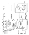
- the control circuit 136 samples the MESSAGE BUFFER TOGGLE signal in the loop 181-182-181, until the signal is deactivated. This is to avoid providing concurrent access to message storage locations to an IOP and to the IOCP, which could result in corruption of data.
- MESSAGE BUFFER TOGGLE signal is deactivated, one of the two exits from the decision 185 is taken, depending upon the code in the function field 142 of the microword. Assume now that the microword is a READ microword requiring the message to be moved from the buffer 99 onto the microcode databus 65 through the bus driver 132b.
- decoder 138 provides a set of signals indicating that the microword is a swap message acceptance register (SMAR) microword.
- SMAR swap message acceptance register
- the microword control circuit waits until the MESSAGE BUFFER TOGGLE signal is deactivated.
- the microcode control circuit operation sequence undertakes a procedure (represented by step 192) to capture the current contents of the MBOR counter 101 in an RT register 193 and to load a new value into the counter 101 by way of an RS register 194. This sequence is initiated by provision, first, of a LOAD RT signal on signal line 197 to a multiplexer 198.
- the IOCP 38 When the IOCP 38 is ready to examine the contents of the buffer 99, data integrity is maintained by execution of a SMAR microword. By this operation, the IOCP swaps the MBOR value in the counter 101 with a value set up by microcode in the RS register 104. Thus, the IOCP gets the address of the last word in the receive message. From this point, it can extract the message. Simultaneously, the MBOR register/counter gets a new value pointing to a section of the buffer 99 which is currently unused. Thus, the IOP receive message entry will not corrupt the message of interest to the IOCP. While the IOCP 38 is interrogating the contents of messages at the MBOR location, receive messages can be received from the bus 39 at the new MBOR value.
Applications Claiming Priority (2)
| Application Number | Priority Date | Filing Date | Title |
|---|---|---|---|
| US29154388A | 1988-12-29 | 1988-12-29 | |
| US291543 | 1988-12-29 |
Publications (2)
| Publication Number | Publication Date |
|---|---|
| EP0375900A2 true EP0375900A2 (fr) | 1990-07-04 |
| EP0375900A3 EP0375900A3 (fr) | 1991-09-18 |
Family
ID=23120735
Family Applications (1)
| Application Number | Title | Priority Date | Filing Date |
|---|---|---|---|
| EP19890120836 Withdrawn EP0375900A3 (fr) | 1988-12-29 | 1989-11-10 | Système ordinateur |
Country Status (2)
| Country | Link |
|---|---|
| EP (1) | EP0375900A3 (fr) |
| JP (1) | JPH065521B2 (fr) |
Cited By (1)
| Publication number | Priority date | Publication date | Assignee | Title |
|---|---|---|---|---|
| EP0550223A2 (fr) * | 1992-01-02 | 1993-07-07 | International Business Machines Corporation | Logique de commande d'arbitrage pour système d'ordinateur avec architecture à double bus |
Citations (1)
| Publication number | Priority date | Publication date | Assignee | Title |
|---|---|---|---|---|
| EP0231595A2 (fr) * | 1985-11-15 | 1987-08-12 | Data General Corporation | Dispositif de commande entrée/sortie pour un système de traitement de données |
-
1989
- 1989-11-10 EP EP19890120836 patent/EP0375900A3/fr not_active Withdrawn
- 1989-11-14 JP JP29407989A patent/JPH065521B2/ja not_active Expired - Lifetime
Patent Citations (1)
| Publication number | Priority date | Publication date | Assignee | Title |
|---|---|---|---|---|
| EP0231595A2 (fr) * | 1985-11-15 | 1987-08-12 | Data General Corporation | Dispositif de commande entrée/sortie pour un système de traitement de données |
Non-Patent Citations (1)
| Title |
|---|
| IBM TECHNICAL DISCLOSURE BULLETIN. vol. 30, no. 4, September 1987, NEW YORK US pages 1591 - 1523; "HIGH SPEED MESSAGE BUFFERS FOR INPUT/OUTPUT PROCESSORS TO MINIMIZE BUFFER NOT-AVAILABLE MESSAGES" * |
Cited By (2)
| Publication number | Priority date | Publication date | Assignee | Title |
|---|---|---|---|---|
| EP0550223A2 (fr) * | 1992-01-02 | 1993-07-07 | International Business Machines Corporation | Logique de commande d'arbitrage pour système d'ordinateur avec architecture à double bus |
| EP0550223A3 (en) * | 1992-01-02 | 1993-09-01 | International Business Machines Corporation | Arbitration control logic for computer system having dual bus architecture |
Also Published As
| Publication number | Publication date |
|---|---|
| JPH02190956A (ja) | 1990-07-26 |
| EP0375900A3 (fr) | 1991-09-18 |
| JPH065521B2 (ja) | 1994-01-19 |
Similar Documents
| Publication | Publication Date | Title |
|---|---|---|
| US4860244A (en) | Buffer system for input/output portion of digital data processing system | |
| US5448702A (en) | Adapters with descriptor queue management capability | |
| US4354225A (en) | Intelligent main store for data processing systems | |
| US4949301A (en) | Improved pointer FIFO controller for converting a standard RAM into a simulated dual FIFO by controlling the RAM's address inputs | |
| EP0550164B1 (fr) | Méthode et dispositif d'entrelacement d'opérations d'accès direct en mémoire en canaux-multiples | |
| US4527237A (en) | Data processing system | |
| US4516199A (en) | Data processing system | |
| CA2123447C (fr) | Structure d'interruption evolutive pour systeme multiprocesseur | |
| US5133062A (en) | RAM buffer controller for providing simulated first-in-first-out (FIFO) buffers in a random access memory | |
| US5001624A (en) | Processor controlled DMA controller for transferring instruction and data from memory to coprocessor | |
| US4495571A (en) | Data processing system having synchronous bus wait/retry cycle | |
| US4493034A (en) | Apparatus and method for an operating system supervisor in a data processing system | |
| US3964054A (en) | Hierarchy response priority adjustment mechanism | |
| US4318174A (en) | Multi-processor system employing job-swapping between different priority processors | |
| JPH02168341A (ja) | データ処理システム | |
| US4415970A (en) | Cache/disk subsystem with load equalization | |
| US5210828A (en) | Multiprocessing system with interprocessor communications facility | |
| JPH04312160A (ja) | マルチプロセッサシステムおよびそのメッセージ送受信制御装置 | |
| US6061757A (en) | Handling interrupts by returning and requeuing currently executing interrupts for later resubmission when the currently executing interrupts are of lower priority than newly generated pending interrupts | |
| US5524211A (en) | System for employing select, pause, and identification registers to control communication among plural processors | |
| EP0037424A1 (fr) | Systeme de traitement de donnees | |
| US5455918A (en) | Data transfer accelerating apparatus and method | |
| CA1169574A (fr) | Multiplexeur de communications a deux microprocesseurs | |
| EP0375900A2 (fr) | Système ordinateur | |
| US4665481A (en) | Speeding up the response time of the direct multiplex control transfer facility |
Legal Events
| Date | Code | Title | Description |
|---|---|---|---|
| PUAI | Public reference made under article 153(3) epc to a published international application that has entered the european phase |
Free format text: ORIGINAL CODE: 0009012 |
|
| AK | Designated contracting states |
Kind code of ref document: A2 Designated state(s): DE FR GB |
|
| 17P | Request for examination filed |
Effective date: 19901025 |
|
| PUAL | Search report despatched |
Free format text: ORIGINAL CODE: 0009013 |
|
| AK | Designated contracting states |
Kind code of ref document: A3 Designated state(s): DE FR GB |
|
| STAA | Information on the status of an ep patent application or granted ep patent |
Free format text: STATUS: THE APPLICATION IS DEEMED TO BE WITHDRAWN |
|
| 18D | Application deemed to be withdrawn |
Effective date: 19930602 |