EP0375272B1 - Coherent phase shift keyed demodulator - Google Patents
Coherent phase shift keyed demodulator Download PDFInfo
- Publication number
- EP0375272B1 EP0375272B1 EP89313062A EP89313062A EP0375272B1 EP 0375272 B1 EP0375272 B1 EP 0375272B1 EP 89313062 A EP89313062 A EP 89313062A EP 89313062 A EP89313062 A EP 89313062A EP 0375272 B1 EP0375272 B1 EP 0375272B1
- Authority
- EP
- European Patent Office
- Prior art keywords
- phase
- carrier signal
- components
- phase angle
- input
- Prior art date
- Legal status (The legal status is an assumption and is not a legal conclusion. Google has not performed a legal analysis and makes no representation as to the accuracy of the status listed.)
- Expired - Lifetime
Links
Images


Classifications
-
- H—ELECTRICITY
- H04—ELECTRIC COMMUNICATION TECHNIQUE
- H04L—TRANSMISSION OF DIGITAL INFORMATION, e.g. TELEGRAPHIC COMMUNICATION
- H04L27/00—Modulated-carrier systems
- H04L27/18—Phase-modulated carrier systems, i.e. using phase-shift keying
- H04L27/22—Demodulator circuits; Receiver circuits
- H04L27/227—Demodulator circuits; Receiver circuits using coherent demodulation
- H04L27/2275—Demodulator circuits; Receiver circuits using coherent demodulation wherein the carrier recovery circuit uses the received modulated signals
Description
- The present invention relates to apparatus for demodulating phase modulated carrier signals, and, although not limited thereto, particularly to modems for transmitting and receiving digital data via communications network such as telephone networks.
- EP-A-0-349-185, which claims a priority date before but was published after the priority date of this specification describes that one type of phase modulation data transmission systems is a differential detection system which detects transmitted data by looking at changes in the phase of input differential phase modulated carrier signal.
- Briefly, two basic methods (or systems) are known for demodulating a differential phase modulated carrier signal; a coherent method and non-coherent method.
- In the coherent method, a carrier recovery circuit is used to reconstruct in-phase and quadrature-phase reference signals which are multiplied against the received signal and phase shifted version of the received signal. The results are then linearly combined to produce a pair of demodulated signals representing the two modulation components of the received signal. In the non-coherent demodulation method, no carrier recovery circuit is used. Instead, a delayed version of the received signal is multiplied against the received signal to produce the demodulated signal.
- Non-coherent demodulation has the advantage of being simple to implement, as it does not require a carrier recovery circuit. Moreover, the input filtering is less complex since a phase splitting filter is not required to generate the complex form of the received signal. However, for the non-coherent method, typically a post detection filter is needed to eliminate double frequency terms generated by the multiplication process. In digital signal processing (where demodulating functions are performed using digital number values obtained from a periodic sampling of the received signal) the coherent method becomes more attractive because many of the calculations can be done at the symbol or baud rate which may range from approximately 600 Hz to 2400 Hz. Digital implementation of the non-coherent method requires operations at the higher sampling rate of at least 8 Hz, for the post detection filter.
- EP-A-0-349-185 discloses that estimates of the in-phase and quadrature-phase components of the input demodulated carrier signal may be used in the demodulation process for generating a so-called "pseudo-coherent" demodulator. To do this, the EP-A-0-349-185 device has the structure of a typical coherent demodulator, but does not have any carrier recovery circuits, using instead the instantaneous estimates of the input carrier signal components. These carrier estimates are obtained directly from the received carrier signal, with a delay of one baud between the calculation of the carrier estimates and their use in the demodulator, for effecting a differential phase shifted demodulated signal at the output of the demodulator.
- Although this demodulator is "pseudo-coherent", the fact remains that it still is not coherent per se. Therefore, in order to obtain better signal-to-noise ratios and better modem performance, a coherent demodulator is still deemed desirable.
- US Patent 4,466,108 describes a demodulator for demodulating a phase modulated input carrier signal. The received phase modulated signal is demodulated before the phase error is determined. The base band signal is then sampled to determine the phase error which, in turn, is used to correct the samples.
- "Open Loop Frequency Synchronization of MDPSK with Doppler" by D.Divsalar in IEEE International Conference on Communications, 7-10 June 1987, Vol.1, p.232-238 describes a Doppler-shifted differential detector for a phase modulated signal. The detector includes a Doppler estimation portion in which in-phase and quadrature phase components of a phase modulated input carrier signal is means for sampling demodulator for demodulating a phase modulated carrier signal are correlated with the input. The correlated signals are then sampled, accumulated, and integrated to produce an estimate of the Doppler shift. Sine and Cosines of the estimate are then used to remove the Doppler shift form the in-phase and quadrature detection channels.
- In accordance with the present invention, there is now provided a demodulator for demodulating a phase modulated input carrier signal, comprising: conversion means for sampling an input carrier signal at baud periods, converting each sample of the input carrier signal into a binary input word representative of the amplitude of input carrier signal at the moment of sampling, and generating in-phase and quadrature-phase components for a current sample of the input carrier signal; first control means for comparing the in-phase and quadrature-phase components of the current sample with corresponding stored ideal components of an existing sample of the input carrier signal to determine phase angle deviation between the current components and ideal components;
second control means for summing the phase deviation with a phase angle of the existing sample and phase shift proportional to the differential phase shift between the baud period in which the current sample was taken and the baud period from which the existing sample was taken to effect a new phase angle for deriving new ideal components of the input carrier signal for comparing with a next sample of the input carrier signal thereby phase-locking the stored ideal components of the input carrier signal in a steady state, and thereby incrementally effecting coherently demodulated and substantially ideal in phase and quadrature-phase components of the input carrier signal. - The present invention provides for a demodulator which uses estimates of the in-phase (or cosine) and quadrature-phase (or sine) components as inputs into a carrier recovery mechanism in order to derive the proper phase and to average out any instantaneous variations in the in-phase and quadrature-phase components, in order to obtain improved signal-to-noise ratios and to have a structure which can be switched from non-coherent to coherent signal processing.
- To achieve this end, the instantaneous carrier estimates are input to a carrier recovery circuit and compared with ideal components which have pre-existing phase angles for generating a phase error signal, i.e. a phase angle deviation between the instantaneous estimates of the components and the ideal components, which then is combined with a pre-existing phase angle and a phase shift for generating a new phase angle. The newly generated phase angle is then used as an input to a sine table which, in response to the new phase angle, outputs new ideal sine and cosine components, to be fed back and compared with the phase error signal. By means of this feedback, the phase error signal is incrementally decreased, thereby eventually leading to substantially ideal sine and cosine components, which are fed to multiplier and adder means, to be recovered as a coherent demodulated carrier signal, minus any phase angle deviations.
- Inasmuch as the coherent demodulator of the invention uses instantaneous estimates of the components of a sample of the input carrier signal, it, like the "pseudo- coherent" demodulator of EP-A-0 349 185, is able to operate at the baud rate, instead of the sampling rate.
- It is, therefore, an objective of the present invention to provide a coherent phase shift keyed demodulator that can be implemented simply and can sample at the baud rate.
- It is another objective of the present invention to provide a coherent demodulator that has an enhanced signal-to-noise ratio and is an extension of the so-called "pseudo-coherent" demodulator.
- The above-mentioned objectives and advantages of the present invention will become more apparent and the invention itself will be best understood by reference to the following description of an embodiment of the invention taken in conjunction with the accompanying drawings, wherein:
-
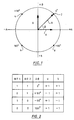
- Figure 1 is a vector diagram of a phase modulated carrier signal to be input to the demodulator of the present invention;
- Figure 2 is a chart used in conjunction with the Figure 1 vector diagram and the demodulator of the present invention to explain the operation of the same;
- Figure 3 is a circuit block diagram showing a digital embodiment of a demodulator constructed in accordance with the present invention;
- Figure 4 is a block diagram showing a representative embodiment of the vital processor hardware which may be used to implement or execute the functions of the Figure 3 digital embodiment;
- Figure 5 is a timing diagram showing typical signal waveforms that may occur at different points at the Figure 3 embodiment; and
- Figure 6 is a circuit block diagram showing an analog embodiment of a demodulator constructed in accordance with the present invention.
- Referring to Figure 1, there is shown a vector diagram of a carrier signal R which is to be input to the demodulator of the present invention. This carrier signal is a four-phase type signal, which means that at any given moment its phase angle may be at any one of four different values. The received carrier signal R is sinusoidal in nature and may be described by the following mathematical relationship:

where
- The symbol "f" denotes the frequency of the carrier signal and "t" denotes time.
- With reference to Figure 1, it can be seen that the outer end of vector R may be located at any one of four
points 2, 4, 6 and 8, at any given instant that Θ is a multiple of 2π. The peak magnitude "C" (in Equation 1) of vector R is represented by the length of the vector, i.e. the radius of the circle in Figure 1; and the instantaneous amplitude of R is represented by its projection onto the real (horizontal) axis. The angle "φ" denotes the phase difference between the transmitted signal R and the reference signal cosine Θ. - The first part of the
Equation 1 describes the received carrier signal R in terms of its in-phase and quadrature-phase components. The in-phase component (cosine Θ) lies on the horizontal axis in Figure 1 and has a peak amplitude value of "A", which is equal to either +1 or -1, depending on the value of the data being transmitted at that moment. The quadrature-phase component (sine Θ) lies along the vertical axis of Figure 1 and has a peak amplitude value of "B", which is equal to +1 or -1, depending on the value of the data being transmitted. It should be appreciated that the vector addition of the in-phase and quadrature-phase components produces the received carrier signal R in Figure 1. - For the four-phase type signal, the data bits to be transmitted are divided into, or organized as, pairs of bits (sometimes also called "dibits"). One pair of the data bits is transmitted during each transmission interval, or baud period. The first bit in each data bit pair determines the amplitude value A of the in-phase component cos Θ while the second data bit in each pair determines the amplitude value B of the quadrature-phase component sin Θ.
- Since each of the amplitude values A and B is binary in nature, i.e. having a value of either +1 or -1, there are four possible phase angles, or phase values, for the carrier signal R. These phase angles are represented by the four
points 2, 4, 6 and 8 shown in Figure 1. In effect, the first data bit in each dibit pair modulates the in-phase component and the second data bit of each dibit pair modulates the quadrature-phase component of the carrier signal R. - In a fixed reference type of phase modulation system, each of the four possible phase angles for the carrier signal R would represent a different two-bit binary value. However, for a differential phase demodulator, such as that of the instant invention, it is not the actual phase angle at any given moment that determines the two-bit binary value, but rather it is the change in phase angle from one transmission interval (baud period) to the next which determines the two-bit binary value.
- The relationship between two-bit binary values being transmitted and the resulting phase angles (φ) which are used to represent such two-bit values is shown in Figure 2. Thus, for example, if the carrier signal R has the same value in a second baud period as it had in the immediately preceding baud period (zero degree phase change), a two-bit binary data value of (1,1) is represented. Similarly, a +90° phase change from one baud period to the next represents a two-bit binary value of (0,1). The amount of phase change from one baud period to the next, therefore, determines the binary values of the two-bit pair.
- This background having been given, attention is directed to Figure 3 wherein a digital embodiment of the demodulator of the present invention is shown. Although shown as discrete components in the embodiment of Fig. 3, it should be appreciated that each of these components may also be interpreted or replaced in other embodiments by functions to be performed, for example, as microcodes in a microprocessor.
- As shown in Fig. 3, a phase modulated carrier signal R is input to a sampling means, such as an analog-to-
digital converter 10. The analog input carrier signal is then converted by analog-to-digital converter 10 into a multi-bit input carrier signal which is transmitted to first and second bandpass filters 12 and 14. As is apparent, analog-to-digital converter 10 periodically samples input carrier signal R and produces for each sample a multi-bit input carrier number representing the amplitude value of the input carrier signal R at the moment of sampling. Thus, there appears at the output of analog-to-digital converter 10 a continuous stream of multi-bit binary numbers, varying in the same manner as the amplitude of the input phase modulator carrier signal R. These discrete digital number values represent the amplitude values at periodically spaced points on the analog waveform. - These bits are fed to digital bandpass filters 12 and 14, which may be of the finite impulse response (FIR) type.
Filter 12 in essence filters out extraneous noise and signals that are beyond its bandwidth so that only the original transmitted signal (in the form of a multi-bit signal) is output therefrom as R. The output fromfilter 14, likewise, is the original transmitted signal, but with a phase shift of 90°. Implementingfilter 14 can be accomplished by means of well known sine and cosine transformations for non-integrating phase shifting of the output signal fromfilter 14 relative to that fromfilter 12. The output offilter 14 is represented as the signal S. - The respective signals R and S are fed to corresponding
dividers 

where R and S are the real and imaginary components, i.e. the in-phase and quadrature-phase components, of the received signal; Ts is the sample period; and P represents a phase offset between the actual carrier and the sampling instant nTs. - Although referred to as the instantaneous estimates of the cosine and sine components, it should be appreciated that these estimates are only valid toward the center of the baud period, and are represented respectively by y and x in Figure 3.
- In EP-A-0 349 185 the instantaneous estimates x and y are sent directly to multipliers and adders, such as
multipliers 24 to 30 andadders 32 and 34. - For the present invention, however, the instantaneous estimates of the in-phase and quadrature-phase of the input carrier signal, output from subtracter 20 and adder 22, which together with
dividers estimator circuit 36 enclosed by dotted lines, are fed to a differential carrier recovery mechanism, designated 38. - Specifically, the instantaneous estimates x and y are fed into a
computational block 40 which has twomultipliers subtracter 46. - The x and y components, when they are input to
computational block 40, have information regarding only the sine and cosine components of the input carrier signal. Incomputational block 40, the x and y components are multiplied and combined according to the following equation:
where A represents the coherent carrier phase Θ and B represents the phase implied inEquations 2 and 3. - It should be noted that the phase implied in
Equations 2 and 3 is never calculated directly via inverse sine and cosine functions since Equation 4 does not require the actual sine and cosine angles. The actual phase error, or phase angle deviation, can be found by taking the sine of the phase error found in Equation 4, and performing an inverse sine function on the value via a table lookup or other possible methods. This process, however, can be avoided by noting that for small angles, the sine of the angle is approximately equal to the magnitude of the angle, in radian measure. Therefore, as the recovered carrier approaches the actual phase of the transmitted carrier, Equation 4 becomes a very good estimate of the actual phase error of the carrier, and thus can be used for adjusting the carrier phase to achieve a very accurate phase synchronization. This phase error is output fromcomputational block 40, vialine 48, and fed into amultiplier 50, which acts as a scaler for multiplying the phase error with a multiplication factor D. - The reason for requiring a
multiplier 50 is that when the phase error is first output from computational block (for instance when the system is first initiated) it tends to be very large. The invention employs a convergence process so this large phase error can be incrementally decreased, by means of feedback. While Equation 4, at the beginning of its computation, is an invalid expression of the actual phase error, the sign of the output phase error does correspond to the sign of the actual phase error. Hence, continuously converging the phase error (or phase angle deviation) output fromcomputational block 40, with some ideal numbers, the phase error eventually will be corrected to reflect the actual phase error. - To achieve this feedback, the scaled phase error is sent next to a
summer 52 which has as its inputs, besides the scaled phase error signal (from multiplier 50), a phase angle from an existing sample of the input carrier signal and a phase shift proportional to the differential phase shift between the baud period in which the current sample of the input carrier signal was taken and the baud period in which the existing sample of the input carrier was taken. The phase shift is represented by the expression Q(n·Ts), which is determined from the output of the demodulator, represented by U and V, as shown in Fig. 2. In other words, the expression Q(n·Ts) is the actual differential phase shift detected by the demodulator. The carrier phase Θ may be obtained from a standard first order loop which tracks the phase error as follows:
- The actual differential phase shift Q(n·Ts) must be added to the coherent carrier phase in order for the instantaneous estimates X and Y to be in-phase with the recovered carrier. This phase shift is also needed if the demodulator is to generate differential phase shifts directly. Alternately, a carrier signal may be maintained without a phase shift being used in demodulating absolute phase shifted signals, and the running phase shift term, Q, may be kept separately and added to the carrier phase for calculation of the phase error, and then taken away afterwards. In Equation 5, E(n·Ts) represents the phase error signal defined by the following equation:

where Equation 6 was obtained by the substitution ofEquations 2 and 3 into Equation 4. - During the initial convergence, the coherent demodulation process cannot provide a valid output phase shift, Q. Therefore, a "pseudo-coherent" demodulator such as that disclosed in the EP-A-0 349 185 is used to provide initial estimates of the phase shifts. After the initiation of the phase convergence, the demodulator can be switched (by either conventional firmware or software, not shown) to a coherent mode in order to obtain better performance.
- Continuing with Fig. 3, it can be seen that the phase angle Θ′ output from
summer 52 is fed to a delay line 54, which may be implemented as a memory. Delay line 54 insures that the new phase angle Θ′ output ofsummer 52 has in fact, as part of its calculation, the existing angle Θ which was provided as an output by delay line 54 and fed back tosummer 52, by means of feed backline 56. The separation of new phase angle Θ′ and phase angle Θ is by one baud period. Accordingly, as new phase angles Θ′ are constantly being produced bysummer 52, constantly updated phase angle Θ are led back tosummer 52, thereby effecting an averaging circuit for incrementally decreasing the phase error signal fromcomputational block 40. - The phase angle Θ is next fed to a sine table 58 which may be a memory or a collection of memories. Although not limited thereto, for this embodiment, phase angle Θ is assumed to have an eight bit value (since it is in a digital format), and the eight bit value of Θ is used as an address for selecting one of, for example, 256 possible entries (or trigonometric functions) which had previously been stored in sine table 58. Thus, in response to a new phase angle Θ, sine table 58 provides a corresponding trigonometric function comprising sine and cosine components to
line computational block 40. - These sine and cosine components from sine table 58, although being multi-bit numbers, actually do represent the amplitudes of the sine wave and cosine wave of the input carrier signal at the phase angle Θ which has just been provided as an input to sine table 58. These sine and cosine waveforms are coherent, although it must be kept in mind that they only represent one sample of the sine wave and one sample of the cosine wave for their particular baud period; and it takes a plurality of these components to fully represent the sine and cosine wave of the input carrier signal.
- The coherent sine and cosine components are next fed to
multipliers adder 32 and subtracter 34 to provide output components U and V, as represented in Fig. 2 and defined by the equations below.

- With reference to Fig. 2, it can be seen the U and V represent the amplitude values of the modulation components of the input carrier signal R. For example, when U equals +1 and V equals +1, a zero (0) degree phase shift is represented. If, in the next baud period, a U of -1 and a V of +1 are obtained, then it can be said that a phase shift of +90°, corresponding to an information dibit pair of (0,1) has been detected. The dibit information, of course, relates to the actual data information that is being conveyed by the analog input carrier signal R, which is to be sent for additional processing, as for example to a slicer whose output may be fed back to
summer block 52 as Q(n·Ts). - The discrete components of the Fig. 3 embodiment can be replaced as functions and be performed by certain specialized digital signal processing (DSP) microprocessors, such as that shown in Fig. 4. In the embodiment of Fig. 4 a
microprocessor 64 is connected through a combination instruction data bus andaddress bus 66 to a number of components. The phase modulated input carrier signal R is fed to an analog-to-digital converter such as 10 shown in Fig. 3. For the Fig. 4 embodiment, the steady stream of multi-bit binary numbers are fed from analog- to-digital converter 10 todata bus 66 and stored in sequential storage locations of a random access read-write memory (RAM) 68. Also included in the Fig. 4 embodiment are a random-access read only memory (ROM) 70 and an input/output interface mechanism 72, which is connected by another data bus 74 to other input/output interface mechanisms. -
Microprocessor 64, in addition to performing other chores, controls the movement of the input carrier multi- bit numbers from analog-to-digit converter 10 toRAM 48. A typical hardware multiplier (not shown) may be added to this type of microprocessor to aid the computation of the different previously discussed equations. Themicroprocessor 64 executes various program routines representing the different functions performed by the components shown in the Fig. 3 embodiment. - These program routines are permanently stored in
ROM 70, which is also coupled tomicroprocessor 64. For example, a first of these function program routines may be analogous to the function performed bybandpass filter 12. A second function program routine may correspond to the function performed byestimator circuit 36, i.e. the earlier discussedEquations 2 and 3. Similarly, a further function program routine may be used for calculating Equation 4, also performed bycomputational block 40 of the Fig. 3 embodiment. Of course, it should be appreciated that these different function program routines are performed in a microcode format and the resulting coherent sine and cosine components of the input carrier signal may still be multiplied and added to form demodulator signal numbers which represent the amplitude values of the input carrier signal, as U and V. - Also, a memory may be partitioned in
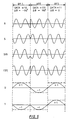
RAM 68 for effecting the delay function of delay block 54, while a portion ofmemory ROM 70 may be reserved for storing the values representing the ideal sine and cosine components stored in sine table 58 of the Fig. 3 embodiment. The resulting demodulator signal numbers U and V are in turn stored inRAM 68 and are to be used for further signal processing operations such as slicing, decoding, descrambling, and deserialization. - Referring to Fig. 5, there is shown a plurality of representative signal patterns at the different outputs of the respective components shown in the Fig. 3 embodiment. The waveforms of Fig. 5 represent three continuous baud periods. As is well known, a baud is a unit of signaling speed and refers to the number of times the state or condition of a signal line may change per second. A baud period is the time interval in which the state or condition of the signal is required to remain the same.
- As shown, the upper waveform in Fig. 5 represents the input carrier signal at the output of
bandpass filter 12; while the second waveform represents the phase shifted signal at the output ofbandpass filter 14. As the cosine and sine components of the carrier signal converge, with short term deviations due to noise being eliminated as a result of the converging process, waveforms representing the coherent sine and cosine components of the carrier signal -- provided as outputs from sine table 58 -- are output, as shown by the middle two waveforms of Fig. 5. As illustrated, the sine and cosine waveforms are shifted by 90° inbaud period BP 2, frombaud period BP 1. Also, even though there is no phase shift betweenbaud period BP 2 and baud period BP 3, there is still a change in the patterns of sine and cosine waveforms for those baud periods based on the phase shift detected inBP 2. - The last two waveform patterns are representative of the amplitude values of the modulation components of the input carrier signal R and, as can be seen at the center of the respective baud periods, U and V do represent the amplitude values of the input carrier signal. For example, for
baud period BP 1, U has a +1 value while in has a -1 value, which correspond to a dibit pair information of (1,0). Likewise inbaud period BP 2, both U and V in have -1 amplitudes. This translates to a dibit pair information of (0,0). As for baud period BP 3, both in U and V have +1 amplitudes values, the dibit pair information contact becoming (1,1). - Although the phase change shown in Fig. 2 and discussed so far relates to a change in the phase angle, an absolute phase may also be used. For the absolute phase scenario, instead of 0°, 90°, 180°, and -90°, corresponding 45°, 135°, 225° and 315° are used. The results remain the same.
- An analog embodiment of the demodulator of the present invention is shown in Fig. 6. For the Fig. 6 embodiment, carrier signal R is fed through a
bandpass filter 76 to asignal distribution line 78. Aphase shifter 80 phase shifts carrier signal R ninety degrees, for generating the signal S. The R and S signals are fed to modulators 82 to 88 and torespective attenuators difference circuits carrier recovery circuit 100, more specifically tomodulators circuit 100. As in earlier embodiments, the input signals are modulated by ideal analog signals, provided in this embodiment by a voltage controlledoscillator 108, in response to a predetermined phase angle Θ. - By means of a
difference circuit 110, the modulated signals from computational block 106 are provided as a phase error signal (or a phase angle deviation) to anamplifier 112, to be multiplied with a constant D. It should be appreciated that D is a fractional constant for assuring that the correction of the phase error signal is only performed in incremental steps, instead of correcting for the entire error in one single step, so that the signal will not become unstable and oscillatory. The thus amplified signal is then summed by a summer 114 with the predetermined phase angle provided by a sample and holdcircuit 116 and a differential phase shift, Q(n·Ts), which is proportional to the differential phase shifts between the input carrier signal and the predetermined input carrier signal. - By thus summing the original
pre-existing phase angle 0 and the current phase shift with the error signal, anew phase angle 0 is calculated and transmitted to sample and holdcircuit 116, from whence anew phase angle 0 is calculated. As before, thisnew phase angle 0 is fed back to summer 114 for further calculations of new phase angles, and to voltage controlledoscillator 108 for providing an input thereto so that ideal cosine and sine waveforms can be output therefrom. The ideal cosine and sine waveforms are fed back byfeedback lines 118 and 120, respectively, to computational block 106, thereby effecting a feedback loop for averaging out the phase error signal. - The thus produced sine and cosine waveforms are next fed, in conjunction with carrier signals R and S, to modulators 82 and 88, paired and added or subtracted by the respective sum and
difference circuits
Claims (10)
- A demodulator for demodulating a phase modulated input carrier signal, comprising:
conversion means (10,12,14) for sampling an input carrier signal (R) at baud periods, converting each sample of the input carrier signal (R) into a binary input word representative of the amplitude of input carrier signal (R) at the moment of sampling, and generating in-phase and quadrature-phase components (R,S) for a current sample of the input carrier signal;
first control means (40) for comparing the in-phase and quadrature-phase components (R,S) of the current sample (R) with corresponding stored ideal components (60,62) of an existing sample of the input carrier signal (R) to determine phase angle deviation (48) between the current components (R,S) and ideal components (60,62); and
second control means (52,54,56,58) for summing the phase deviation (48) with a phase angle (φ) of the existing sample and phase shift (Q(n*Ts)) proportional to the differential phase shift between the baud period in which the current sample was taken and the baud period from which the existing sample was taken to effect a new phase angle (φ′) for deriving new ideal components (COS,SIN) of the input carrier signal (R) for comparing with a next sample of the input carrier signal (R), thereby phase-locking the stored ideal components (COS,SIN) of the input carrier signal (R) in a steady state, and thereby incrementally effecting coherently demodulated and substantially ideal in phase and quadrature-phase components (U,V) of the input carrier signal (R). - A demodulator as claimed in Claim 1, wherein the first control means (40) comprises:
a plurality of multiplier elements (44,42) each multiplying one of the current components (R,5) with a corresponding one of the ideal components (SIN,COS) and; - A demodulator as claimed in Claim 1, comprising:
scaler means (50) for multiplying the phase angle deviation (48) with a fractional correction constant (D). - A demodulator as claimed in Claim 1, wherein the conversion means (10,12,14) comprises:
a first filter (12) for filtering the binary input word to generate a filtered input carrier signal (R) having the same amplitude values as the input carrier signal (R) and;
a second filter (14) for filtering and phase shifting the binary input word to generate a filtered phase shifted carrier signal (S) having the same amplitude values as the input carrier signal (R). - A demodulator as claimed in Claim 1, wherein the second control means (52,54,56,58) comprises:
a first adder (52) for summing the phase angle deviation (48) with the phase angle (56) of the existing sample and the proportional differential phase shift (Q(n*Ts)) and for outputting the new phase angle (φ) and;
a delay element (54) for providing at its output the phase angle (φ) of the existing sample to the first adder (52) and for receiving at its input the new phase angle (φ′) output from the first adder (52), the delay element (54) providing a delay of at least one baud period between the phase angle (φ) output therefrom and the new phase angle (φ′) input thereto. - A demodulator as claimed in Claim 5, further comprising:
a memory (58) responsive to the phase angle (φ) provided at the output of the delay element (54) for outputting stored ideal cosine and sine components (COS,SIN) corresponding to the phase angle output from the delay element (54) whereby the stored cosine and sine components (COS,SIN) are fed back to the first control means to be compared with instantaneous estimates of the in-phase and quadrature-phase components (R,5) of the next sample of the input carrier signal (R). - A demodulator as claimed in Claim 6, further comprising:
multiplier means (24-30) for multiplying the stored cosine and sine components of (COS.SIN) of the input carrier signal (R) corresponding to the phase angle (φ) output from the delay means (54) with the current sample (R,S); and
a second adder (32,34) for summing results of the multiplier means (26,28) provide the coherently demodulated in phase and quadrature-phase components (U,V) of the input carrier signal (R). - A demodulator as claimed in Claim 7, wherein the delay element (54) comprises a sample and hold circuit, and wherein the memory (58) comprises a voltage controlled oscillator.
- A demodulator as claimed in Claim 8, further comprising;
amplifier means (50) for providing a correction gain (D) to the phase angle deviation. - Apparatus as claimed in Claim 1, wherein the second control means (52,54,56.58) comprises:
a memory (58) for outputting a prestored value (SIN,COS) in response to the current phase angle (φ) of the input carrier signal (R) as a feedback to incrementally eliminate the phase angle deviation;
means (24-30) for multiplying the value (SIN,COS) from the memory (58) with the binary input word (R) and a corresponding phase shifted binary input word (S); NP means (32,34) for adding results from the multiplying means (24-30) to generate coherently demodulated in-phase and quadrature-phase components (U,V) of the input carrier signal (R).
Applications Claiming Priority (2)
| Application Number | Priority Date | Filing Date | Title |
|---|---|---|---|
| US289064 | 1988-12-23 | ||
| US07/289,064 US4871974A (en) | 1988-12-23 | 1988-12-23 | Coherent phase shift keyed demodulator |
Publications (3)
| Publication Number | Publication Date |
|---|---|
| EP0375272A2 EP0375272A2 (en) | 1990-06-27 |
| EP0375272A3 EP0375272A3 (en) | 1990-10-31 |
| EP0375272B1 true EP0375272B1 (en) | 1994-09-21 |
Family
ID=23109887
Family Applications (1)
| Application Number | Title | Priority Date | Filing Date |
|---|---|---|---|
| EP89313062A Expired - Lifetime EP0375272B1 (en) | 1988-12-23 | 1989-12-13 | Coherent phase shift keyed demodulator |
Country Status (5)
| Country | Link |
|---|---|
| US (1) | US4871974A (en) |
| EP (1) | EP0375272B1 (en) |
| JP (1) | JPH0666818B2 (en) |
| CA (1) | CA2000007C (en) |
| DE (1) | DE68918421T2 (en) |
Families Citing this family (32)
| Publication number | Priority date | Publication date | Assignee | Title |
|---|---|---|---|---|
| US4849706A (en) * | 1988-07-01 | 1989-07-18 | International Business Machines Corporation | Differential phase modulation demodulator |
| JPH0687541B2 (en) * | 1989-06-22 | 1994-11-02 | シャープ株式会社 | Quadrature amplitude modulation wave demodulator |
| US5134634A (en) * | 1989-08-31 | 1992-07-28 | Nec Corporation | Multilevel quadrature amplitude demodulator capable of compensating for a quadrature phase deviation of a carrier signal pair |
| CA2079422C (en) * | 1991-09-30 | 1996-07-02 | Osamu Ichiyoshi | Phase-locked circuit capable of being quickly put in a phase-locked state |
| US5841816A (en) * | 1992-10-22 | 1998-11-24 | Ericsson Inc. | Diversity Pi/4-DQPSK demodulation |
| US5801895A (en) * | 1996-05-28 | 1998-09-01 | Hewlett Packard Company | Disk drive servo demodulation system which suppresses noise on the position error signal |
| EP1017201A1 (en) * | 1998-12-29 | 2000-07-05 | Alcatel | QAM receiver with separate detection of phase and amplitude |
| US7277494B2 (en) * | 2003-06-04 | 2007-10-02 | Honeywell Federal Manufacturing & Technologies, Llc | Method of differential-phase/absolute-amplitude QAM |
| US7995648B2 (en) * | 2004-04-09 | 2011-08-09 | Trident Microsystems (Far East) Ltd. | Advanced digital receiver |
| US8611408B2 (en) | 2004-04-09 | 2013-12-17 | Entropic Communications, Inc. | Apparatus for and method of developing equalized values from samples of a signal received from a channel |
| US20080298518A1 (en) * | 2004-08-12 | 2008-12-04 | Gopalan Krishnamurthy | Automatic Gain Control Unit of a Receiver |
| US9198608B2 (en) | 2005-04-28 | 2015-12-01 | Proteus Digital Health, Inc. | Communication system incorporated in a container |
| CN101496042A (en) | 2006-05-02 | 2009-07-29 | 普罗秋斯生物医学公司 | Patient customized therapeutic regimens |
| EP2083680B1 (en) | 2006-10-25 | 2016-08-10 | Proteus Digital Health, Inc. | Controlled activation ingestible identifier |
| US8718193B2 (en) * | 2006-11-20 | 2014-05-06 | Proteus Digital Health, Inc. | Active signal processing personal health signal receivers |
| ES2930588T3 (en) | 2007-02-01 | 2022-12-19 | Otsuka Pharma Co Ltd | Ingestible Event Marker Systems |
| KR101528748B1 (en) | 2007-02-14 | 2015-06-15 | 프로테우스 디지털 헬스, 인코포레이티드 | In-body power source having high surface area electrode |
| US8115618B2 (en) | 2007-05-24 | 2012-02-14 | Proteus Biomedical, Inc. | RFID antenna for in-body device |
| DK2192946T3 (en) | 2007-09-25 | 2022-11-21 | Otsuka Pharma Co Ltd | In-body device with virtual dipole signal amplification |
| ES2840773T3 (en) | 2008-03-05 | 2021-07-07 | Otsuka Pharma Co Ltd | Multimode Communication Ingestible Event Markers and Systems |
| SG195535A1 (en) | 2008-07-08 | 2013-12-30 | Proteus Digital Health Inc | Ingestible event marker data framework |
| JP2012514799A (en) | 2009-01-06 | 2012-06-28 | プロテウス バイオメディカル インコーポレイテッド | Methods and systems for ingestion related biofeedback and individual pharmacotherapy |
| TWI517050B (en) | 2009-11-04 | 2016-01-11 | 普羅托斯數位健康公司 | System for supply chain management |
| TWI557672B (en) | 2010-05-19 | 2016-11-11 | 波提亞斯數位康健公司 | Computer system and computer-implemented method to track medication from manufacturer to a patient, apparatus and method for confirming delivery of medication to a patient, patient interface device |
| EP2538596B1 (en) * | 2011-06-21 | 2014-05-14 | Alcatel Lucent | Method of decoding a differentially encoded phase modulated optical data signal |
| US9756874B2 (en) | 2011-07-11 | 2017-09-12 | Proteus Digital Health, Inc. | Masticable ingestible product and communication system therefor |
| WO2015112603A1 (en) | 2014-01-21 | 2015-07-30 | Proteus Digital Health, Inc. | Masticable ingestible product and communication system therefor |
| MX340001B (en) | 2011-07-21 | 2016-06-20 | Proteus Digital Health Inc | Mobile communication device, system, and method. |
| CN104181558A (en) * | 2013-05-24 | 2014-12-03 | 凹凸电子(武汉)有限公司 | GPS receiver and method for judging tracking loop state of GPS receiver |
| EP3005281A4 (en) | 2013-06-04 | 2017-06-28 | Proteus Digital Health, Inc. | System, apparatus and methods for data collection and assessing outcomes |
| US10084880B2 (en) | 2013-11-04 | 2018-09-25 | Proteus Digital Health, Inc. | Social media networking based on physiologic information |
| BR112019000861B1 (en) | 2016-07-22 | 2020-10-27 | Proteus Digital Health, Inc | electronic device |
Family Cites Families (22)
| Publication number | Priority date | Publication date | Assignee | Title |
|---|---|---|---|---|
| GB1431119A (en) * | 1973-05-04 | 1976-04-07 | Siemens Ag | Data transmission systems |
| DE2354718C3 (en) * | 1973-11-02 | 1981-12-17 | Licentia Patent-Verwaltungs-Gmbh, 6000 Frankfurt | Demodulation method for phase-shift keyed oscillations and circuit arrangement for carrying out the method |
| FR2368184A1 (en) * | 1976-10-18 | 1978-05-12 | Ibm France | CARRIER SYNCHRONIZATION SYSTEM FOR COHERENT PHASE DEMODULATOR |
| US4169246A (en) * | 1976-12-06 | 1979-09-25 | Motorola, Inc. | Digital carrier correction circuit |
| JPS5580950A (en) * | 1978-12-08 | 1980-06-18 | Fujitsu Ltd | Arrier wave regenerating circuit |
| US4206320A (en) * | 1978-08-21 | 1980-06-03 | University Of Illinois Foundation | High speed modem suitable for operating with a switched network |
| US4224575A (en) * | 1978-11-29 | 1980-09-23 | E-Systems, Inc. | Phase/frequency controlled phase shift keyed signal carrier reconstruction circuit |
| US4246654A (en) * | 1979-01-09 | 1981-01-20 | Northrop Corporation | Digital coherent phase demodulator |
| US4328587A (en) * | 1979-02-19 | 1982-05-04 | Kokusai Denshin Denwa Kabushiki Kaisha | Phase slip detector and systems employing the detector |
| US4379266A (en) * | 1980-04-03 | 1983-04-05 | Ford Aerospace & Communications Corporation | PSK Demodulator with automatic compensation of delay induced phase shifts |
| US4313205A (en) * | 1980-07-07 | 1982-01-26 | Communications Satellite Corporation | Carrier synchronization and symbol synchronization for offset-QPSK burst communications |
| US4461014A (en) * | 1980-09-23 | 1984-07-17 | Mitsubishi Denki Kabushiki Kaisha | Carrier regenerating circuit |
| US4397039A (en) * | 1980-12-29 | 1983-08-02 | International Business Machines Corporation | Instantaneous phase tracking in single sideband systems |
| US4423390A (en) * | 1981-01-09 | 1983-12-27 | Harris Corporation | Side lock avoidance network for PSK demodulator |
| JPS5825746A (en) * | 1981-08-10 | 1983-02-16 | Fujitsu Ltd | Carrier wave reproducing circuit |
| US4466108A (en) * | 1981-10-06 | 1984-08-14 | Communications Satellite Corporation | TDMA/PSK Carrier synchronization without preamble |
| US4457005A (en) * | 1981-12-07 | 1984-06-26 | Motorola, Inc. | Digital coherent PSK demodulator and detector |
| JPS58114654A (en) * | 1981-12-28 | 1983-07-08 | Fujitsu Ltd | Reproducing circuit of reference carrier wave |
| US4670887A (en) * | 1985-08-05 | 1987-06-02 | Hayes Microcomputer Products, Inc. | Multiplexed PSK demodulator |
| US4740997A (en) * | 1985-08-05 | 1988-04-26 | Hayes Microcomputer Products, Inc. | Band clock offset phase locked loop |
| US4712221A (en) * | 1986-08-29 | 1987-12-08 | International Business Machines Corporation | Carrier recovery of modulated signals |
| US4849706A (en) * | 1988-07-01 | 1989-07-18 | International Business Machines Corporation | Differential phase modulation demodulator |
-
1988
- 1988-12-23 US US07/289,064 patent/US4871974A/en not_active Expired - Fee Related
-
1989
- 1989-10-02 CA CA002000007A patent/CA2000007C/en not_active Expired - Fee Related
- 1989-12-13 DE DE68918421T patent/DE68918421T2/en not_active Expired - Fee Related
- 1989-12-13 EP EP89313062A patent/EP0375272B1/en not_active Expired - Lifetime
- 1989-12-15 JP JP1324163A patent/JPH0666818B2/en not_active Expired - Lifetime
Also Published As
| Publication number | Publication date |
|---|---|
| JPH0666818B2 (en) | 1994-08-24 |
| US4871974A (en) | 1989-10-03 |
| CA2000007C (en) | 1994-10-25 |
| CA2000007A1 (en) | 1990-06-23 |
| EP0375272A3 (en) | 1990-10-31 |
| DE68918421T2 (en) | 1995-03-30 |
| DE68918421D1 (en) | 1994-10-27 |
| JPH02219339A (en) | 1990-08-31 |
| EP0375272A2 (en) | 1990-06-27 |
Similar Documents
| Publication | Publication Date | Title |
|---|---|---|
| EP0375272B1 (en) | Coherent phase shift keyed demodulator | |
| JP2526931B2 (en) | PSK signal demodulator | |
| US5838737A (en) | Method and apparatus for estimating PSK modulated signals | |
| JP2643792B2 (en) | Demodulator | |
| CA2025232C (en) | Carrier recovery system | |
| JP3728573B2 (en) | Demodulator | |
| EP0639914B1 (en) | MSK phase acquisition and tracking method | |
| JPH0552101B2 (en) | ||
| US5581582A (en) | Automatic frequency control method and apparatus therefor | |
| US6075408A (en) | OQPSK phase and timing detection | |
| EP0413153B1 (en) | Quadrature phase demodulation using a training sequence and a local signal offset from the received carrier frequency | |
| US4054838A (en) | QAM phase jitter and frequency offset correction system | |
| US5627861A (en) | Carrier phase estimation system using filter | |
| EP0349185B1 (en) | Demodulating phase modulated carrier signal | |
| US6996191B1 (en) | Efficient accurate controller for envelope feedforward power amplifiers | |
| JP3517056B2 (en) | Sampling timing phase error detector for VSB modulated signal | |
| AU678950B2 (en) | Digital demodulator | |
| US5090027A (en) | Coherent PSK demodulator with adaptive line enhancer | |
| EP0154503A2 (en) | Digital signal processor | |
| US4942592A (en) | Synchronous receiver for minimum shift keying transmission | |
| EP0484914B1 (en) | Demodulator and method for demodulating digital signals modulated by a minimum shift keying | |
| US4439737A (en) | Phase locked loop, as for MPSK signal detector | |
| JP3148090B2 (en) | OFDM signal synchronous demodulator | |
| JP3479882B2 (en) | Demodulator | |
| JPH06237277A (en) | Psk carrier signal regenerating device |
Legal Events
| Date | Code | Title | Description |
|---|---|---|---|
| PUAI | Public reference made under article 153(3) epc to a published international application that has entered the european phase |
Free format text: ORIGINAL CODE: 0009012 |
|
| AK | Designated contracting states |
Kind code of ref document: A2 Designated state(s): DE FR GB |
|
| PUAL | Search report despatched |
Free format text: ORIGINAL CODE: 0009013 |
|
| AK | Designated contracting states |
Kind code of ref document: A3 Designated state(s): DE FR GB |
|
| 17P | Request for examination filed |
Effective date: 19910618 |
|
| 17Q | First examination report despatched |
Effective date: 19930604 |
|
| GRAA | (expected) grant |
Free format text: ORIGINAL CODE: 0009210 |
|
| AK | Designated contracting states |
Kind code of ref document: B1 Designated state(s): DE FR GB |
|
| REF | Corresponds to: |
Ref document number: 68918421 Country of ref document: DE Date of ref document: 19941027 |
|
| ET | Fr: translation filed | ||
| PLBE | No opposition filed within time limit |
Free format text: ORIGINAL CODE: 0009261 |
|
| STAA | Information on the status of an ep patent application or granted ep patent |
Free format text: STATUS: NO OPPOSITION FILED WITHIN TIME LIMIT |
|
| 26N | No opposition filed | ||
| PGFP | Annual fee paid to national office [announced via postgrant information from national office to epo] |
Ref country code: GB Payment date: 19951127 Year of fee payment: 7 |
|
| PGFP | Annual fee paid to national office [announced via postgrant information from national office to epo] |
Ref country code: FR Payment date: 19951128 Year of fee payment: 7 |
|
| PGFP | Annual fee paid to national office [announced via postgrant information from national office to epo] |
Ref country code: DE Payment date: 19951229 Year of fee payment: 7 |
|
| PG25 | Lapsed in a contracting state [announced via postgrant information from national office to epo] |
Ref country code: GB Effective date: 19961213 |
|
| GBPC | Gb: european patent ceased through non-payment of renewal fee |
Effective date: 19961213 |
|
| PG25 | Lapsed in a contracting state [announced via postgrant information from national office to epo] |
Ref country code: FR Effective date: 19970829 |
|
| PG25 | Lapsed in a contracting state [announced via postgrant information from national office to epo] |
Ref country code: DE Effective date: 19970902 |
|
| REG | Reference to a national code |
Ref country code: FR Ref legal event code: ST |