EP0361652A2 - Perforated through-coated plastic sheets - Google Patents
Perforated through-coated plastic sheets Download PDFInfo
- Publication number
- EP0361652A2 EP0361652A2 EP89307434A EP89307434A EP0361652A2 EP 0361652 A2 EP0361652 A2 EP 0361652A2 EP 89307434 A EP89307434 A EP 89307434A EP 89307434 A EP89307434 A EP 89307434A EP 0361652 A2 EP0361652 A2 EP 0361652A2
- Authority
- EP
- European Patent Office
- Prior art keywords
- plastic
- perforations
- sheet
- sheet product
- plastic sheet
- Prior art date
- Legal status (The legal status is an assumption and is not a legal conclusion. Google has not performed a legal analysis and makes no representation as to the accuracy of the status listed.)
- Withdrawn
Links
- 239000002985 plastic film Substances 0.000 title claims abstract description 42
- 239000002131 composite material Substances 0.000 claims abstract description 29
- 229910052751 metal Inorganic materials 0.000 claims description 60
- 239000002184 metal Substances 0.000 claims description 60
- 239000000758 substrate Substances 0.000 claims description 33
- 239000004033 plastic Substances 0.000 claims description 30
- 229920003023 plastic Polymers 0.000 claims description 30
- 238000000576 coating method Methods 0.000 claims description 16
- 238000000034 method Methods 0.000 claims description 16
- 239000011248 coating agent Substances 0.000 claims description 15
- 229920001721 polyimide Polymers 0.000 claims description 9
- 239000004642 Polyimide Substances 0.000 claims description 8
- 229920000642 polymer Polymers 0.000 claims description 6
- -1 polyacrylic Polymers 0.000 claims description 4
- 229920001601 polyetherimide Polymers 0.000 claims description 4
- 239000004593 Epoxy Substances 0.000 claims description 3
- 239000004952 Polyamide Substances 0.000 claims description 3
- 229920002492 poly(sulfone) Polymers 0.000 claims description 3
- 229920002647 polyamide Polymers 0.000 claims description 3
- 239000004417 polycarbonate Substances 0.000 claims description 3
- 229920000515 polycarbonate Polymers 0.000 claims description 3
- 229920000728 polyester Polymers 0.000 claims description 3
- 239000011159 matrix material Substances 0.000 claims 7
- 239000004697 Polyetherimide Substances 0.000 claims 2
- 150000003949 imides Chemical class 0.000 claims 1
- 239000002952 polymeric resin Substances 0.000 claims 1
- 239000012783 reinforcing fiber Substances 0.000 claims 1
- 229920003002 synthetic resin Polymers 0.000 claims 1
- 239000003292 glue Substances 0.000 abstract description 4
- 230000032798 delamination Effects 0.000 abstract description 2
- 239000010408 film Substances 0.000 description 39
- 239000000047 product Substances 0.000 description 31
- 239000000463 material Substances 0.000 description 17
- 238000004080 punching Methods 0.000 description 10
- 238000000151 deposition Methods 0.000 description 9
- 239000011347 resin Substances 0.000 description 9
- 229920005989 resin Polymers 0.000 description 9
- PXHVJJICTQNCMI-UHFFFAOYSA-N Nickel Chemical compound [Ni] PXHVJJICTQNCMI-UHFFFAOYSA-N 0.000 description 8
- 150000002739 metals Chemical class 0.000 description 8
- 229920006255 plastic film Polymers 0.000 description 7
- 150000001875 compounds Chemical class 0.000 description 6
- 238000001755 magnetron sputter deposition Methods 0.000 description 5
- VYZAMTAEIAYCRO-UHFFFAOYSA-N Chromium Chemical compound [Cr] VYZAMTAEIAYCRO-UHFFFAOYSA-N 0.000 description 4
- 241000208822 Lactuca Species 0.000 description 4
- 235000003228 Lactuca sativa Nutrition 0.000 description 4
- 229910052804 chromium Inorganic materials 0.000 description 4
- 239000011651 chromium Substances 0.000 description 4
- 230000008021 deposition Effects 0.000 description 4
- 150000002736 metal compounds Chemical class 0.000 description 4
- 229910052759 nickel Inorganic materials 0.000 description 4
- 229920003223 poly(pyromellitimide-1,4-diphenyl ether) Polymers 0.000 description 4
- 230000001681 protective effect Effects 0.000 description 4
- 238000004544 sputter deposition Methods 0.000 description 4
- WEVYAHXRMPXWCK-UHFFFAOYSA-N Acetonitrile Chemical compound CC#N WEVYAHXRMPXWCK-UHFFFAOYSA-N 0.000 description 3
- 239000000805 composite resin Substances 0.000 description 3
- 239000013615 primer Substances 0.000 description 3
- 239000002987 primer (paints) Substances 0.000 description 3
- 229910052814 silicon oxide Inorganic materials 0.000 description 3
- 239000000243 solution Substances 0.000 description 3
- JOYRKODLDBILNP-UHFFFAOYSA-N Ethyl urethane Chemical compound CCOC(N)=O JOYRKODLDBILNP-UHFFFAOYSA-N 0.000 description 2
- KDLHZDBZIXYQEI-UHFFFAOYSA-N Palladium Chemical compound [Pd] KDLHZDBZIXYQEI-UHFFFAOYSA-N 0.000 description 2
- VYPSYNLAJGMNEJ-UHFFFAOYSA-N Silicium dioxide Chemical compound O=[Si]=O VYPSYNLAJGMNEJ-UHFFFAOYSA-N 0.000 description 2
- GWEVSGVZZGPLCZ-UHFFFAOYSA-N Titan oxide Chemical compound O=[Ti]=O GWEVSGVZZGPLCZ-UHFFFAOYSA-N 0.000 description 2
- 230000002411 adverse Effects 0.000 description 2
- 238000005266 casting Methods 0.000 description 2
- 238000005229 chemical vapour deposition Methods 0.000 description 2
- 238000009730 filament winding Methods 0.000 description 2
- 150000002500 ions Chemical class 0.000 description 2
- 238000001465 metallisation Methods 0.000 description 2
- 239000000203 mixture Substances 0.000 description 2
- BASFCYQUMIYNBI-UHFFFAOYSA-N platinum Chemical compound [Pt] BASFCYQUMIYNBI-UHFFFAOYSA-N 0.000 description 2
- 229920000647 polyepoxide Polymers 0.000 description 2
- 238000002360 preparation method Methods 0.000 description 2
- 239000010703 silicon Substances 0.000 description 2
- 239000010409 thin film Substances 0.000 description 2
- OGIDPMRJRNCKJF-UHFFFAOYSA-N titanium oxide Inorganic materials [Ti]=O OGIDPMRJRNCKJF-UHFFFAOYSA-N 0.000 description 2
- 206010059837 Adhesion Diseases 0.000 description 1
- 229920002799 BoPET Polymers 0.000 description 1
- 229910001369 Brass Inorganic materials 0.000 description 1
- RYGMFSIKBFXOCR-UHFFFAOYSA-N Copper Chemical compound [Cu] RYGMFSIKBFXOCR-UHFFFAOYSA-N 0.000 description 1
- 229910000599 Cr alloy Inorganic materials 0.000 description 1
- YUBJPYNSGLJZPQ-UHFFFAOYSA-N Dithiopyr Chemical compound CSC(=O)C1=C(C(F)F)N=C(C(F)(F)F)C(C(=O)SC)=C1CC(C)C YUBJPYNSGLJZPQ-UHFFFAOYSA-N 0.000 description 1
- 239000005041 Mylar™ Substances 0.000 description 1
- 229920000784 Nomex Polymers 0.000 description 1
- 239000004698 Polyethylene Substances 0.000 description 1
- BLRPTPMANUNPDV-UHFFFAOYSA-N Silane Chemical compound [SiH4] BLRPTPMANUNPDV-UHFFFAOYSA-N 0.000 description 1
- XUIMIQQOPSSXEZ-UHFFFAOYSA-N Silicon Chemical compound [Si] XUIMIQQOPSSXEZ-UHFFFAOYSA-N 0.000 description 1
- BQCADISMDOOEFD-UHFFFAOYSA-N Silver Chemical compound [Ag] BQCADISMDOOEFD-UHFFFAOYSA-N 0.000 description 1
- 229920001646 UPILEX Polymers 0.000 description 1
- 230000001464 adherent effect Effects 0.000 description 1
- 239000002318 adhesion promoter Substances 0.000 description 1
- 239000002998 adhesive polymer Substances 0.000 description 1
- 229910045601 alloy Inorganic materials 0.000 description 1
- 239000000956 alloy Substances 0.000 description 1
- 229910052782 aluminium Inorganic materials 0.000 description 1
- XAGFODPZIPBFFR-UHFFFAOYSA-N aluminium Chemical compound [Al] XAGFODPZIPBFFR-UHFFFAOYSA-N 0.000 description 1
- PNEYBMLMFCGWSK-UHFFFAOYSA-N aluminium oxide Inorganic materials [O-2].[O-2].[O-2].[Al+3].[Al+3] PNEYBMLMFCGWSK-UHFFFAOYSA-N 0.000 description 1
- 239000010951 brass Substances 0.000 description 1
- 239000003054 catalyst Substances 0.000 description 1
- 238000005234 chemical deposition Methods 0.000 description 1
- 239000000788 chromium alloy Substances 0.000 description 1
- 230000001427 coherent effect Effects 0.000 description 1
- 238000009734 composite fabrication Methods 0.000 description 1
- 238000010276 construction Methods 0.000 description 1
- 229910052802 copper Inorganic materials 0.000 description 1
- 239000010949 copper Substances 0.000 description 1
- 238000005520 cutting process Methods 0.000 description 1
- 239000003989 dielectric material Substances 0.000 description 1
- KPUWHANPEXNPJT-UHFFFAOYSA-N disiloxane Chemical class [SiH3]O[SiH3] KPUWHANPEXNPJT-UHFFFAOYSA-N 0.000 description 1
- 230000000694 effects Effects 0.000 description 1
- 125000003700 epoxy group Chemical group 0.000 description 1
- 239000003822 epoxy resin Substances 0.000 description 1
- 238000005530 etching Methods 0.000 description 1
- 239000012467 final product Substances 0.000 description 1
- YBMRDBCBODYGJE-UHFFFAOYSA-N germanium oxide Inorganic materials O=[Ge]=O YBMRDBCBODYGJE-UHFFFAOYSA-N 0.000 description 1
- PCHJSUWPFVWCPO-UHFFFAOYSA-N gold Chemical compound [Au] PCHJSUWPFVWCPO-UHFFFAOYSA-N 0.000 description 1
- 229910052737 gold Inorganic materials 0.000 description 1
- 239000010931 gold Substances 0.000 description 1
- 230000003116 impacting effect Effects 0.000 description 1
- 238000010348 incorporation Methods 0.000 description 1
- APFVFJFRJDLVQX-UHFFFAOYSA-N indium atom Chemical compound [In] APFVFJFRJDLVQX-UHFFFAOYSA-N 0.000 description 1
- 229910003437 indium oxide Inorganic materials 0.000 description 1
- 238000001659 ion-beam spectroscopy Methods 0.000 description 1
- 238000003475 lamination Methods 0.000 description 1
- 229910044991 metal oxide Inorganic materials 0.000 description 1
- 150000004706 metal oxides Chemical class 0.000 description 1
- 239000011104 metalized film Substances 0.000 description 1
- 230000003278 mimic effect Effects 0.000 description 1
- 150000004767 nitrides Chemical class 0.000 description 1
- 239000004763 nomex Substances 0.000 description 1
- 238000010943 off-gassing Methods 0.000 description 1
- 239000003973 paint Substances 0.000 description 1
- 229910052763 palladium Inorganic materials 0.000 description 1
- 238000007747 plating Methods 0.000 description 1
- 229910052697 platinum Inorganic materials 0.000 description 1
- 229920000573 polyethylene Polymers 0.000 description 1
- 239000009719 polyimide resin Substances 0.000 description 1
- 238000007639 printing Methods 0.000 description 1
- 230000001737 promoting effect Effects 0.000 description 1
- 229910000077 silane Inorganic materials 0.000 description 1
- 229910021332 silicide Inorganic materials 0.000 description 1
- 229910052710 silicon Inorganic materials 0.000 description 1
- 229910052709 silver Inorganic materials 0.000 description 1
- 239000004332 silver Substances 0.000 description 1
- 239000007921 spray Substances 0.000 description 1
- 229910001256 stainless steel alloy Inorganic materials 0.000 description 1
- 239000000126 substance Substances 0.000 description 1
- 229920002803 thermoplastic polyurethane Polymers 0.000 description 1
- XOLBLPGZBRYERU-UHFFFAOYSA-N tin dioxide Chemical compound O=[Sn]=O XOLBLPGZBRYERU-UHFFFAOYSA-N 0.000 description 1
- 229910001887 tin oxide Inorganic materials 0.000 description 1
- 150000003673 urethanes Chemical class 0.000 description 1
- 238000001771 vacuum deposition Methods 0.000 description 1
Images
Classifications
-
- B—PERFORMING OPERATIONS; TRANSPORTING
- B29—WORKING OF PLASTICS; WORKING OF SUBSTANCES IN A PLASTIC STATE IN GENERAL
- B29D—PRODUCING PARTICULAR ARTICLES FROM PLASTICS OR FROM SUBSTANCES IN A PLASTIC STATE
- B29D7/00—Producing flat articles, e.g. films or sheets
- B29D7/01—Films or sheets
-
- B—PERFORMING OPERATIONS; TRANSPORTING
- B29—WORKING OF PLASTICS; WORKING OF SUBSTANCES IN A PLASTIC STATE IN GENERAL
- B29C—SHAPING OR JOINING OF PLASTICS; SHAPING OF MATERIAL IN A PLASTIC STATE, NOT OTHERWISE PROVIDED FOR; AFTER-TREATMENT OF THE SHAPED PRODUCTS, e.g. REPAIRING
- B29C70/00—Shaping composites, i.e. plastics material comprising reinforcements, fillers or preformed parts, e.g. inserts
- B29C70/88—Shaping composites, i.e. plastics material comprising reinforcements, fillers or preformed parts, e.g. inserts characterised primarily by possessing specific properties, e.g. electrically conductive or locally reinforced
- B29C70/882—Shaping composites, i.e. plastics material comprising reinforcements, fillers or preformed parts, e.g. inserts characterised primarily by possessing specific properties, e.g. electrically conductive or locally reinforced partly or totally electrically conductive, e.g. for EMI shielding
- B29C70/885—Shaping composites, i.e. plastics material comprising reinforcements, fillers or preformed parts, e.g. inserts characterised primarily by possessing specific properties, e.g. electrically conductive or locally reinforced partly or totally electrically conductive, e.g. for EMI shielding with incorporated metallic wires, nets, films or plates
-
- B—PERFORMING OPERATIONS; TRANSPORTING
- B29—WORKING OF PLASTICS; WORKING OF SUBSTANCES IN A PLASTIC STATE IN GENERAL
- B29C—SHAPING OR JOINING OF PLASTICS; SHAPING OF MATERIAL IN A PLASTIC STATE, NOT OTHERWISE PROVIDED FOR; AFTER-TREATMENT OF THE SHAPED PRODUCTS, e.g. REPAIRING
- B29C2793/00—Shaping techniques involving a cutting or machining operation
- B29C2793/0045—Perforating
-
- B—PERFORMING OPERATIONS; TRANSPORTING
- B29—WORKING OF PLASTICS; WORKING OF SUBSTANCES IN A PLASTIC STATE IN GENERAL
- B29K—INDEXING SCHEME ASSOCIATED WITH SUBCLASSES B29B, B29C OR B29D, RELATING TO MOULDING MATERIALS OR TO MATERIALS FOR MOULDS, REINFORCEMENTS, FILLERS OR PREFORMED PARTS, e.g. INSERTS
- B29K2105/00—Condition, form or state of moulded material or of the material to be shaped
- B29K2105/06—Condition, form or state of moulded material or of the material to be shaped containing reinforcements, fillers or inserts
-
- B—PERFORMING OPERATIONS; TRANSPORTING
- B29—WORKING OF PLASTICS; WORKING OF SUBSTANCES IN A PLASTIC STATE IN GENERAL
- B29K—INDEXING SCHEME ASSOCIATED WITH SUBCLASSES B29B, B29C OR B29D, RELATING TO MOULDING MATERIALS OR TO MATERIALS FOR MOULDS, REINFORCEMENTS, FILLERS OR PREFORMED PARTS, e.g. INSERTS
- B29K2995/00—Properties of moulding materials, reinforcements, fillers, preformed parts or moulds
- B29K2995/0003—Properties of moulding materials, reinforcements, fillers, preformed parts or moulds having particular electrical or magnetic properties, e.g. piezoelectric
- B29K2995/0005—Conductive
-
- Y—GENERAL TAGGING OF NEW TECHNOLOGICAL DEVELOPMENTS; GENERAL TAGGING OF CROSS-SECTIONAL TECHNOLOGIES SPANNING OVER SEVERAL SECTIONS OF THE IPC; TECHNICAL SUBJECTS COVERED BY FORMER USPC CROSS-REFERENCE ART COLLECTIONS [XRACs] AND DIGESTS
- Y10—TECHNICAL SUBJECTS COVERED BY FORMER USPC
- Y10T—TECHNICAL SUBJECTS COVERED BY FORMER US CLASSIFICATION
- Y10T156/00—Adhesive bonding and miscellaneous chemical manufacture
- Y10T156/10—Methods of surface bonding and/or assembly therefor
- Y10T156/1052—Methods of surface bonding and/or assembly therefor with cutting, punching, tearing or severing
- Y10T156/1054—Methods of surface bonding and/or assembly therefor with cutting, punching, tearing or severing and simultaneously bonding [e.g., cut-seaming]
-
- Y—GENERAL TAGGING OF NEW TECHNOLOGICAL DEVELOPMENTS; GENERAL TAGGING OF CROSS-SECTIONAL TECHNOLOGIES SPANNING OVER SEVERAL SECTIONS OF THE IPC; TECHNICAL SUBJECTS COVERED BY FORMER USPC CROSS-REFERENCE ART COLLECTIONS [XRACs] AND DIGESTS
- Y10—TECHNICAL SUBJECTS COVERED BY FORMER USPC
- Y10T—TECHNICAL SUBJECTS COVERED BY FORMER US CLASSIFICATION
- Y10T156/00—Adhesive bonding and miscellaneous chemical manufacture
- Y10T156/10—Methods of surface bonding and/or assembly therefor
- Y10T156/1052—Methods of surface bonding and/or assembly therefor with cutting, punching, tearing or severing
- Y10T156/1056—Perforating lamina
- Y10T156/1057—Subsequent to assembly of laminae
-
- Y—GENERAL TAGGING OF NEW TECHNOLOGICAL DEVELOPMENTS; GENERAL TAGGING OF CROSS-SECTIONAL TECHNOLOGIES SPANNING OVER SEVERAL SECTIONS OF THE IPC; TECHNICAL SUBJECTS COVERED BY FORMER USPC CROSS-REFERENCE ART COLLECTIONS [XRACs] AND DIGESTS
- Y10—TECHNICAL SUBJECTS COVERED BY FORMER USPC
- Y10T—TECHNICAL SUBJECTS COVERED BY FORMER US CLASSIFICATION
- Y10T428/00—Stock material or miscellaneous articles
- Y10T428/24—Structurally defined web or sheet [e.g., overall dimension, etc.]
- Y10T428/24273—Structurally defined web or sheet [e.g., overall dimension, etc.] including aperture
- Y10T428/24281—Struck out portion type
-
- Y—GENERAL TAGGING OF NEW TECHNOLOGICAL DEVELOPMENTS; GENERAL TAGGING OF CROSS-SECTIONAL TECHNOLOGIES SPANNING OVER SEVERAL SECTIONS OF THE IPC; TECHNICAL SUBJECTS COVERED BY FORMER USPC CROSS-REFERENCE ART COLLECTIONS [XRACs] AND DIGESTS
- Y10—TECHNICAL SUBJECTS COVERED BY FORMER USPC
- Y10T—TECHNICAL SUBJECTS COVERED BY FORMER US CLASSIFICATION
- Y10T428/00—Stock material or miscellaneous articles
- Y10T428/24—Structurally defined web or sheet [e.g., overall dimension, etc.]
- Y10T428/24273—Structurally defined web or sheet [e.g., overall dimension, etc.] including aperture
- Y10T428/24298—Noncircular aperture [e.g., slit, diamond, rectangular, etc.]
- Y10T428/24314—Slit or elongated
-
- Y—GENERAL TAGGING OF NEW TECHNOLOGICAL DEVELOPMENTS; GENERAL TAGGING OF CROSS-SECTIONAL TECHNOLOGIES SPANNING OVER SEVERAL SECTIONS OF THE IPC; TECHNICAL SUBJECTS COVERED BY FORMER USPC CROSS-REFERENCE ART COLLECTIONS [XRACs] AND DIGESTS
- Y10—TECHNICAL SUBJECTS COVERED BY FORMER USPC
- Y10T—TECHNICAL SUBJECTS COVERED BY FORMER US CLASSIFICATION
- Y10T428/00—Stock material or miscellaneous articles
- Y10T428/24—Structurally defined web or sheet [e.g., overall dimension, etc.]
- Y10T428/24273—Structurally defined web or sheet [e.g., overall dimension, etc.] including aperture
- Y10T428/24322—Composite web or sheet
-
- Y—GENERAL TAGGING OF NEW TECHNOLOGICAL DEVELOPMENTS; GENERAL TAGGING OF CROSS-SECTIONAL TECHNOLOGIES SPANNING OVER SEVERAL SECTIONS OF THE IPC; TECHNICAL SUBJECTS COVERED BY FORMER USPC CROSS-REFERENCE ART COLLECTIONS [XRACs] AND DIGESTS
- Y10—TECHNICAL SUBJECTS COVERED BY FORMER USPC
- Y10T—TECHNICAL SUBJECTS COVERED BY FORMER US CLASSIFICATION
- Y10T428/00—Stock material or miscellaneous articles
- Y10T428/24—Structurally defined web or sheet [e.g., overall dimension, etc.]
- Y10T428/24777—Edge feature
-
- Y—GENERAL TAGGING OF NEW TECHNOLOGICAL DEVELOPMENTS; GENERAL TAGGING OF CROSS-SECTIONAL TECHNOLOGIES SPANNING OVER SEVERAL SECTIONS OF THE IPC; TECHNICAL SUBJECTS COVERED BY FORMER USPC CROSS-REFERENCE ART COLLECTIONS [XRACs] AND DIGESTS
- Y10—TECHNICAL SUBJECTS COVERED BY FORMER USPC
- Y10T—TECHNICAL SUBJECTS COVERED BY FORMER US CLASSIFICATION
- Y10T428/00—Stock material or miscellaneous articles
- Y10T428/24—Structurally defined web or sheet [e.g., overall dimension, etc.]
- Y10T428/24802—Discontinuous or differential coating, impregnation or bond [e.g., artwork, printing, retouched photograph, etc.]
- Y10T428/24826—Spot bonds connect components
-
- Y—GENERAL TAGGING OF NEW TECHNOLOGICAL DEVELOPMENTS; GENERAL TAGGING OF CROSS-SECTIONAL TECHNOLOGIES SPANNING OVER SEVERAL SECTIONS OF THE IPC; TECHNICAL SUBJECTS COVERED BY FORMER USPC CROSS-REFERENCE ART COLLECTIONS [XRACs] AND DIGESTS
- Y10—TECHNICAL SUBJECTS COVERED BY FORMER USPC
- Y10T—TECHNICAL SUBJECTS COVERED BY FORMER US CLASSIFICATION
- Y10T428/00—Stock material or miscellaneous articles
- Y10T428/24—Structurally defined web or sheet [e.g., overall dimension, etc.]
- Y10T428/24802—Discontinuous or differential coating, impregnation or bond [e.g., artwork, printing, retouched photograph, etc.]
- Y10T428/24917—Discontinuous or differential coating, impregnation or bond [e.g., artwork, printing, retouched photograph, etc.] including metal layer
-
- Y—GENERAL TAGGING OF NEW TECHNOLOGICAL DEVELOPMENTS; GENERAL TAGGING OF CROSS-SECTIONAL TECHNOLOGIES SPANNING OVER SEVERAL SECTIONS OF THE IPC; TECHNICAL SUBJECTS COVERED BY FORMER USPC CROSS-REFERENCE ART COLLECTIONS [XRACs] AND DIGESTS
- Y10—TECHNICAL SUBJECTS COVERED BY FORMER USPC
- Y10T—TECHNICAL SUBJECTS COVERED BY FORMER US CLASSIFICATION
- Y10T428/00—Stock material or miscellaneous articles
- Y10T428/24—Structurally defined web or sheet [e.g., overall dimension, etc.]
- Y10T428/24942—Structurally defined web or sheet [e.g., overall dimension, etc.] including components having same physical characteristic in differing degree
- Y10T428/2495—Thickness [relative or absolute]
- Y10T428/24967—Absolute thicknesses specified
- Y10T428/24975—No layer or component greater than 5 mils thick
-
- Y—GENERAL TAGGING OF NEW TECHNOLOGICAL DEVELOPMENTS; GENERAL TAGGING OF CROSS-SECTIONAL TECHNOLOGIES SPANNING OVER SEVERAL SECTIONS OF THE IPC; TECHNICAL SUBJECTS COVERED BY FORMER USPC CROSS-REFERENCE ART COLLECTIONS [XRACs] AND DIGESTS
- Y10—TECHNICAL SUBJECTS COVERED BY FORMER USPC
- Y10T—TECHNICAL SUBJECTS COVERED BY FORMER US CLASSIFICATION
- Y10T428/00—Stock material or miscellaneous articles
- Y10T428/26—Web or sheet containing structurally defined element or component, the element or component having a specified physical dimension
- Y10T428/263—Coating layer not in excess of 5 mils thick or equivalent
- Y10T428/264—Up to 3 mils
- Y10T428/265—1 mil or less
-
- Y—GENERAL TAGGING OF NEW TECHNOLOGICAL DEVELOPMENTS; GENERAL TAGGING OF CROSS-SECTIONAL TECHNOLOGIES SPANNING OVER SEVERAL SECTIONS OF THE IPC; TECHNICAL SUBJECTS COVERED BY FORMER USPC CROSS-REFERENCE ART COLLECTIONS [XRACs] AND DIGESTS
- Y10—TECHNICAL SUBJECTS COVERED BY FORMER USPC
- Y10T—TECHNICAL SUBJECTS COVERED BY FORMER US CLASSIFICATION
- Y10T428/00—Stock material or miscellaneous articles
- Y10T428/26—Web or sheet containing structurally defined element or component, the element or component having a specified physical dimension
- Y10T428/266—Web or sheet containing structurally defined element or component, the element or component having a specified physical dimension of base or substrate
-
- Y—GENERAL TAGGING OF NEW TECHNOLOGICAL DEVELOPMENTS; GENERAL TAGGING OF CROSS-SECTIONAL TECHNOLOGIES SPANNING OVER SEVERAL SECTIONS OF THE IPC; TECHNICAL SUBJECTS COVERED BY FORMER USPC CROSS-REFERENCE ART COLLECTIONS [XRACs] AND DIGESTS
- Y10—TECHNICAL SUBJECTS COVERED BY FORMER USPC
- Y10T—TECHNICAL SUBJECTS COVERED BY FORMER US CLASSIFICATION
- Y10T428/00—Stock material or miscellaneous articles
- Y10T428/31—Surface property or characteristic of web, sheet or block
-
- Y—GENERAL TAGGING OF NEW TECHNOLOGICAL DEVELOPMENTS; GENERAL TAGGING OF CROSS-SECTIONAL TECHNOLOGIES SPANNING OVER SEVERAL SECTIONS OF THE IPC; TECHNICAL SUBJECTS COVERED BY FORMER USPC CROSS-REFERENCE ART COLLECTIONS [XRACs] AND DIGESTS
- Y10—TECHNICAL SUBJECTS COVERED BY FORMER USPC
- Y10T—TECHNICAL SUBJECTS COVERED BY FORMER US CLASSIFICATION
- Y10T428/00—Stock material or miscellaneous articles
- Y10T428/31504—Composite [nonstructural laminate]
- Y10T428/31507—Of polycarbonate
-
- Y—GENERAL TAGGING OF NEW TECHNOLOGICAL DEVELOPMENTS; GENERAL TAGGING OF CROSS-SECTIONAL TECHNOLOGIES SPANNING OVER SEVERAL SECTIONS OF THE IPC; TECHNICAL SUBJECTS COVERED BY FORMER USPC CROSS-REFERENCE ART COLLECTIONS [XRACs] AND DIGESTS
- Y10—TECHNICAL SUBJECTS COVERED BY FORMER USPC
- Y10T—TECHNICAL SUBJECTS COVERED BY FORMER US CLASSIFICATION
- Y10T428/00—Stock material or miscellaneous articles
- Y10T428/31504—Composite [nonstructural laminate]
- Y10T428/31511—Of epoxy ether
- Y10T428/31529—Next to metal
-
- Y—GENERAL TAGGING OF NEW TECHNOLOGICAL DEVELOPMENTS; GENERAL TAGGING OF CROSS-SECTIONAL TECHNOLOGIES SPANNING OVER SEVERAL SECTIONS OF THE IPC; TECHNICAL SUBJECTS COVERED BY FORMER USPC CROSS-REFERENCE ART COLLECTIONS [XRACs] AND DIGESTS
- Y10—TECHNICAL SUBJECTS COVERED BY FORMER USPC
- Y10T—TECHNICAL SUBJECTS COVERED BY FORMER US CLASSIFICATION
- Y10T428/00—Stock material or miscellaneous articles
- Y10T428/31504—Composite [nonstructural laminate]
- Y10T428/31533—Of polythioether
-
- Y—GENERAL TAGGING OF NEW TECHNOLOGICAL DEVELOPMENTS; GENERAL TAGGING OF CROSS-SECTIONAL TECHNOLOGIES SPANNING OVER SEVERAL SECTIONS OF THE IPC; TECHNICAL SUBJECTS COVERED BY FORMER USPC CROSS-REFERENCE ART COLLECTIONS [XRACs] AND DIGESTS
- Y10—TECHNICAL SUBJECTS COVERED BY FORMER USPC
- Y10T—TECHNICAL SUBJECTS COVERED BY FORMER US CLASSIFICATION
- Y10T428/00—Stock material or miscellaneous articles
- Y10T428/31504—Composite [nonstructural laminate]
- Y10T428/31678—Of metal
- Y10T428/31681—Next to polyester, polyamide or polyimide [e.g., alkyd, glue, or nylon, etc.]
-
- Y—GENERAL TAGGING OF NEW TECHNOLOGICAL DEVELOPMENTS; GENERAL TAGGING OF CROSS-SECTIONAL TECHNOLOGIES SPANNING OVER SEVERAL SECTIONS OF THE IPC; TECHNICAL SUBJECTS COVERED BY FORMER USPC CROSS-REFERENCE ART COLLECTIONS [XRACs] AND DIGESTS
- Y10—TECHNICAL SUBJECTS COVERED BY FORMER USPC
- Y10T—TECHNICAL SUBJECTS COVERED BY FORMER US CLASSIFICATION
- Y10T428/00—Stock material or miscellaneous articles
- Y10T428/31504—Composite [nonstructural laminate]
- Y10T428/31678—Of metal
- Y10T428/31692—Next to addition polymer from unsaturated monomers
- Y10T428/31699—Ester, halide or nitrile of addition polymer
Definitions
- This invention relates to metallized plastic film products and their use in composite structures.
- this invention relates to electrically conductive films and their use in shaped composite structures.
- a typical product produced heretofore is a plastic body or a plastic film having a metal layer on one or both sides.
- the usual film product is a continuous sheet product.
- the metallized plastic sheet material may be desired to incorporate into laminated composite structures.
- the metallized sheet can provide an electrically conductive surface or impart other useful metal properties to the composite. While conventional metallized plastic sheet products have been used in these applications, they have two inherent characteristics which interfere with their acceptability in high performance areas.
- the first of these two problems is that the metallized plastic layers, being continuous plastic sheets, have difficulty conforming to complex or compound curves. This can be solved in some cases by tailoring the sheet to fit the object to which it is being laminated or by folding the sheet to conform. So too, a stretchable continuous substrate can also give some degree of conformance to the complex compound curves. However, these solutions are far from ideal. The cutting and folding approaches can be extremely labor intensive. They also can introduce or give rise to breaks in the film's metal coating which can degrade or destroy desired electrical properties. The use of stretchable substrates presents the problem that the metal coating often is less able to stretch than the substrate and thus breaks or separates from the substrate.
- the second problem relates to the strength of the adhesion between either the metal layer and the substrate, the composite resin and the metal layer, or the composite resin and the plastic substrate. Often, the grip between these surfaces is relatively poor. This can be a significant problem when the material is incorporated into laminates because the boundary between the plastic sheet or the metal coated on the sheet and the surrounding composite resin can serve as shear planes which can disrupt or defeat the strength of the overall laminate structure.
- the perforations add significant drape or formability to the plastic sheets so that they can be formed into compound curves and the like.
- the perforations can be applied in a controlled manner as needed to adjust the sheet resistivity of the product or to give a variable sheet resistivity from point to point on the sheet.
- the perforations can take the form of slits, so as to give a "lettuce wrap" type product or they can take the form of holes punched through the plastic/metal sheet product.
- the electrically conductive metal layer is a sputter-deposited layer especially one having a thickness of from about 5 nm to about 500 nm.
- this inventicn provides composite structures incorporating the perforated sheet film.
- this invention provides a method of forming the perforated sheet films in which the plastic substrate is coated with the conductive metal layer and thereafter subjected to perforation such as by slitting or by punching.
- the product of this invention is a plastic sheet or film having an electrically conductive layer on one or both surfaces and containing perforations through the conductive layer and the plastic sheet.
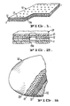
- a simple embodiment of this product is shown in Fig. 1 as sheet 10.
- Sheet 10 includes a plastic substrate 11 having deposited on its surface a conductive metal layer 12 and having a plurality of perforations 13 and 13A. As can be seen with reference to perforation 13A, the perforations extend through the metal layer and the plastic substrate.
- plastic sheet 11 is shown in discontinuous section. This is done to illustrate the fact that the plastic substrate is many times thicker than the metal layer 12. Typically, the substrate is on the order of several mils in thickness and the metal layer is on the order of nanometers in thickness.
- the sheet products of this invention may contain additional layers, as well.
- sheet product 20 as shown in Fig. 2, an additional layer is present.
- This layer, 21, is an adherent protective liner film.
- This layer is provided as physical protection for the very thin metallic film. It assures the integrity of the metal layer and prevents it from becoming scratched during handling and the like. It is removed prior to composite fabrication.
- the products of this invention can contain a variety of other optional layers, if desired.
- Fig 3. shows a compound curved housing 30 which employs the metallized plastic layer 10 of this invention in its construction.
- Housing 30 includes filament winding 31 and a casting resin 32/33.
- the resin shown as 32 and 33 impregnates the filament winding and glues through the layer 10 so as to give a continuous body of resin. This assures the strength of the product and prevents delamination at the metallized or plastic sheet surfaces.
- the plastic film employed in the metallized sheets of this invention is an essentially two dimensioned sheet. Included within the definition of films and sheets as used herein are fabric-like materials and "paper"-like materials. Typical films are from about 0.25 to about 20 mil thick. Thicker or thinner materials may be used, if desired. Preferably the film is from about .5 mils to about 5 mils thick and is a plastic roll stock. It will be appreciated that the primary function of the film is to provide a substrate for the metal layer it carries. Therefore, it is not always necessary to use a film that has special properties or characteristics.
- the exact nature of the film can be set, in part, by the nature of the metal deposition employed. It is important to select a film that is compatible with the metallizing method. For example, if a chemical deposition method is used, the film should be compatible with the deposition chemistry and environment. Similarly, if a vacuum deposition method such as sputtering or ion deposition is used, the substrate film should be able to withstand the deposition temperatures and be able to be used without substantial outgassing or the like at the high vacuum conditions employed. Similarly, the substrate should not detract from the properties of the overall composite in its environment of use. For example, if the composite is to be placed in a thermally hostile environment, the substrate should be such as to withstand it.
- Typical plastics include the polyesters and in particular the polyethylene terphthalates marketed under trademarks such as Mylar, Melinex, Hostaphan and the like; another group of representative substrates are the polyimides marketed under trademarks such as Kapton, Upilex, Novax, and Apical. Other forms of polyimide such as Nomex "paper” sheets can be employed as well. Some of these materials such as polyimides, polysulfones, and polyetherimides are suitable materials if high temperature stability is an issue as they are known to have good thermal performance properties.
- any polymer which is capable of withstanding the conditions of metallizing can be used, these include polyacrylics, polycarbonates, polyamides and polyetherimides. In general these systems will withstand the conditions of the preferred metal deposition method which is vacuum sputtering. This process will often reach temperatures of 150°C, etc.
- the polyimides, such as the Kapton material are very suitable and in our experience preferred.
- the metal layers carried on the plastic sheets are thin films. These layers are referred to as "metal" layers for simplicity but can include within this term mixtures of metals, metal compounds and mixtures of metals and metal compounds.
- the films typically have a thickness of from about 5 nm to about 2,000 nm and preferably from about 5 nm to about 1,000 nm. If desired, multi-layered metal structures can be laid down such as layers of different metals or combination of metals and dielectrics.
- the reasons for incorporating the metal layers into the final composites are often electrical in nature, such as to impart a given conductivity to a structure, to impart impedance matching properties to a structure, or the like. Accordingly, it is often desired to define the "metal" layers in terms of their electrical properties, in particular their sheet resistivities.
- Typical sheet resistivities can range from less than 1 ohm per square to about 2000 ohms per square.
- Preferred sheet resistivities range from about 10 ohms per square to about 1500 ohms per square.
- Typical materials for incorporation into the products as the metal layer include the conductive metals such as copper, gold, silver, aluminum, nickel, platinum, palladium, chromium or the like.
- mixed metals can be laid down, for example, nickel/chromium alloys, stainless steel alloys, brass, and the like.
- Representative metal compounds include various metal oxides, suboxides, silicides, nitrides and the like.
- the metal layer can be applied to one or both sides of the plastic substrate. This points up one major advantage of the present invention that the general configuration of the metal-coated plastic substrate can be varied widely without adversely impacting the properties of the final product as a direct result of the perforations called for herein.
- a plurality of metal layers can be used, separated, if desired, from one another by intervening layers, such as layers of dielectric or the like.
- These additional layers can be in the form of a sputter-deposited or the like thin layers or they can be in the form of one or more thick "macrolayers" (that is, a layer similar in thickness to the plastic substrate) such as a protective or adhesive polymer layer or tackifier applied over the metal layer.
- a dielectric layer it can be selected from materials having a bulk resistivity of greater than 5 ohm centimeters such as silicon, silicon oxide, silicon oxide/titanium oxide, alumina, titanium oxide, silicon/germanium oxide, indium/ tin oxide and the like. These dielectric layers can be laid down by various thin layer deposition methods such as sputter depositing.
- macrolayer layers When macrolayer layers are added this can be done by various lamination, printing, or spray methods.
- Typical macrolayers include protective hardcoats such as epoxy or siloxane hardcoats, adhesion promoters and primers such as silane primers, and plastic over coats such as urethanes, epoxies, and the like.
- a key to the present invention is the presence of perforations through the metallized plastic sheet.
- These perforations can take the form of slits so as to give a "lettuce wrap" type product or they can take the form of holes punched through the film. If holes are used, they can take up as much as 75% or even 90% of the surface area of this sheet, if desired.
- the size of the holes can be controlled, and are end use application specific. In a preferred embodiment, the largest dimension of the holes should not exceed about 1 millimeter. At the lower end, hole size is controlled by the hole punching process. Typically, holes are larger than about 0.1 millimeters. This lower number should not be considered a strict limit however, as other equivalent sizes can be used as well. In many applications, there seems to be equivalent performance with holes this small and holes as large as about 1 mm. In view of the relative ease of punching the larger holes, they are generally preferred, unless their size compromises end use performance.
- the slits should be no longer than about a centimeter or two. In addition, they should be spaced no more than about a centimeter apart. Preferably, they are from about 0.5 mm long to about 2 mm long and spaced about 0.5 to about 1 mm apart.
- the perforations of this invention can serve a number of useful purposes, each of which can lead to highly advantageous properties and products.
- the perforations provide "glue through" opportunities so that the plastic film does not serve as a shear plane in a high strength composite.
- the resin employed is generally a conventional composite forming resin such as an epoxy resin, a urethane resin or a polyimide resin such as the high temperature bismaleimide-type resins known in the art.
- the perforations serve to increase the drape and conformability of the film. This permits the film to be more easily conformed into complex and/or complicated shapes.
- the perforating of the film also provides an additional and unrelated advantage which finds application in a wide range of applications not encompassed by composite-forming.
- This advantage is that it increases the sheet resistance of the film.
- resistivity resistance
- hole punching may be preferable to slitting as it allows the actual removal of metal layer from the sheet product.
- the increase in resistance can be used to adjust the resistance of the film very precisely. It can also be used to increase resistances by as much as a factor of 3 to 5 or so. It can also be used to give a variable resistance across or along a sheet of metallized film.
- the films of this invention are generally made in a two-step process.
- the conductive metal layer is laid down on a continuous nonperforated sheet of film.
- the film is perforated either by slitting or by punching. Any conventional perforating system which will give rise to perforations of this size and density described above can in theory be used.
- the method for depositing the metal layer can be selected from any of the physical or chemical methods known in the art for depositing metal layers on plastic sheets. These include chemical vapor deposition, ion beam sputtering, magnetron sputtering and the like. Due to our expertise in the field, we prefer to use magnetron sputtering.
- the metal layer can be laid down with a uniform resistivity or a tapered resistivity prior to perforation, as is well practiced by those in the deposition art.
- a roll of polyimide sheet film 2 mil thick (Kapton) is placed in a continuous-feed magnetron sputtering unit.
- the sputtering unit is equipped with a plurality of nickel/chromium electrodes.
- the polyimide roll stock is fed past the electrodes which are operated in a magnetron sputtering mode so as to continuously deposit a coherent essentially uniform layer of nickel/chromium on the Kapton film.
- the sheet resistivity of the product is measured during lay down and by controlling the electrode conditions and the line speed of the substrate past the electrodes, an average sheet resistance of about 100 ohms/square is achieved.
- the product is then removed from the magnetron sputterer and laminated with a 1 or 2 mil thick release liner.
- One section of this film is then placed in a perforating device and cut into a lettuce wrap configuration with slits approximately 5 millimeters long and 2 millimeters apart. Other portions are subjected to perforation by hole punching.
- the number of holes is varied. In some cases a uniform density of holes is applied. In other cases the arrangement of holes is varied from place to place on the sheet of film. Hole size is varied between about 0.1 and about 5 millimeters with best results being observed when the hole size is held at 1 millimeter diameter or smaller.
- the density of holes ranges from about 1% up to about 90% of the total area of the film.
- the sheet resistivity of the film is measured before and after hole punching. It is seen that the sheet resistance of the film goes up as holes are punched in it. At the highest levels of punching the resistance is increased by as much as fourfold to fivefold compared to the starting film.
- Initial films having sheet resistances of for example 100 ohm/square can be increased in sheet resistance to as much as 500, 600 or even 1,000 ohm/square. This is accomplished by the punching while still having metal layers thick enough to have good physical integrity.
- the sheet products are incorporated into laminated structures. It is seen that both the slit and the punched products have improved drape and are more easily conformed to complex compound curves with minimal wrinkling or puckering. When used in combination with casting resins, these materials provide excellent glue-through and thus excellent strength to the composite. When composites made using the perforated materials are compared with composites made with the same materials in unperforated form, it is seen that substantial strength advantages are achieved by using the perforated materials.
Landscapes
- Engineering & Computer Science (AREA)
- Mechanical Engineering (AREA)
- Chemical & Material Sciences (AREA)
- Composite Materials (AREA)
- Laminated Bodies (AREA)
Abstract
Metallized plastic sheet film products improved by being perforated through their surfaces are disclosed. These sheet products can be incorporated into improved strength composites since their perforations permit glue through and prevent delamination and shear previously observed with metallized plastic sheet film products. In addition, the perforations can be used to adjust the conductivity/resistance of the electrically conductive sheet films.
Description
- This invention relates to metallized plastic film products and their use in composite structures. In a preferred embodiment, this invention relates to electrically conductive films and their use in shaped composite structures.
- It has long been recognized that metallic layers can be deposited on plastic films. Chemical vapor deposition techniques, plating processes, magnetron sputtering and ion sputtering are representative processes for depositing nanometer thick (or thicker) films of metals, metal compounds, and the like on plastic materials such as plastic sheets. A typical product produced heretofore is a plastic body or a plastic film having a metal layer on one or both sides. The usual film product is a continuous sheet product. These sheet products find applications in electronic devices, in windows as light reflectors, and in other applications where a thin sheet of metal is useful.
- In these and many other applications, it may be desired to incorporate the metallized plastic sheet material into laminated composite structures. In these structures, the metallized sheet can provide an electrically conductive surface or impart other useful metal properties to the composite. While conventional metallized plastic sheet products have been used in these applications, they have two inherent characteristics which interfere with their acceptability in high performance areas.
- The first of these two problems is that the metallized plastic layers, being continuous plastic sheets, have difficulty conforming to complex or compound curves. This can be solved in some cases by tailoring the sheet to fit the object to which it is being laminated or by folding the sheet to conform. So too, a stretchable continuous substrate can also give some degree of conformance to the complex compound curves. However, these solutions are far from ideal. The cutting and folding approaches can be extremely labor intensive. They also can introduce or give rise to breaks in the film's metal coating which can degrade or destroy desired electrical properties. The use of stretchable substrates presents the problem that the metal coating often is less able to stretch than the substrate and thus breaks or separates from the substrate.
- The second problem relates to the strength of the adhesion between either the metal layer and the substrate, the composite resin and the metal layer, or the composite resin and the plastic substrate. Often, the grip between these surfaces is relatively poor. This can be a significant problem when the material is incorporated into laminates because the boundary between the plastic sheet or the metal coated on the sheet and the surrounding composite resin can serve as shear planes which can disrupt or defeat the strength of the overall laminate structure.
- One way to address this second problem would be to improve the adhesion of the metal layer to the substrate. Drauglis et al. in USP 4,374,717, issued in 1983, suggest that the adhesion of sputtered chromium to urethane substrates can be improved by applying a coating of plasma polymerized acetonitrile under and over the metal layer. Manabe, et al. in USP 4,369,225, issued in 1983, suggest that an improved metal coating is achieved when the metal is undercoated with a flexible urethane paint and then overcoated with a similar material. Gliem, et al. suggest in USP 4,364,792, issued in 1982, that the adhesion of metals can be improved by etching the surface of the polymer to roughen it prior to coating. Kumagai, et al. show another approach in USP 4,402,998, issued in 1983, when they suggest that a primer coat of metal be laid down, followed by a catalyst layer and finally the desired metal layer. All of these representative disclosures point up the problem with adhesion. Their solutions may work in certain low performance areas, such as decorative coatings and sheltered electronic devices, but they do not suggest that their solutions are adequate in high performance areas where the shear plane can severely detract from the strength of ultrahigh strength composite materials as are found in aircraft and the like.
- When we produced metallized thin films for incorporation into such high performance composite structures, the above-described failings appeared. It is, therefore, an object of this invention to solve these problems presented by prior metallized plastic films.
- A simple but dramatically effective discovery has now been made. It has now been found that a structural sheet product comprising a plastic sheet and having deposited on one or both of its sides a coating comprising an electrically conductive metal layer is improved for use in composites and the like by applying a plurality of perforations through the plastic sheet and the coating. It has been found that these perforations do not adversely effect the bulk electrical properties of the conductive metal layer and permit several advantages to be achieved. For one, ultrahigh strength composite materials can be formed from these sheets and composite-forming resins since the resins can "glue through" the perforations and prevent the metallized sheet from serving as a shear plane. For another, the perforations add significant drape or formability to the plastic sheets so that they can be formed into compound curves and the like. For another, the perforations can be applied in a controlled manner as needed to adjust the sheet resistivity of the product or to give a variable sheet resistivity from point to point on the sheet.
- In accord with the present invention the perforations can take the form of slits, so as to give a "lettuce wrap" type product or they can take the form of holes punched through the plastic/metal sheet product. In a presently preferred embodiment, the electrically conductive metal layer is a sputter-deposited layer especially one having a thickness of from about 5 nm to about 500 nm. In another aspect, this inventicn provides composite structures incorporating the perforated sheet film. In yet another aspect this invention provides a method of forming the perforated sheet films in which the plastic substrate is coated with the conductive metal layer and thereafter subjected to perforation such as by slitting or by punching.
- This invention will be described with reference being made to the accompanying drawings in which
- Fig. 1 is a not-to-scale cut-away perspective view of a plastic sheet product in accord with this invention;
- Fig. 2 is an expanded view, also not to scale, showing a cut-away of a preferred embodiment of the plastic sheet product of this invention; and
- Fig. 3 is a partially cut-away perspective view of a compound curve composite product illustrating one application of the plastic sheet products of this invention.
- The product of this invention is a plastic sheet or film having an electrically conductive layer on one or both surfaces and containing perforations through the conductive layer and the plastic sheet. A simple embodiment of this product is shown in Fig. 1 as
sheet 10.Sheet 10 includes a plastic substrate 11 having deposited on its surface aconductive metal layer 12 and having a plurality ofperforations 13 and 13A. As can be seen with reference to perforation 13A, the perforations extend through the metal layer and the plastic substrate. In this figure, plastic sheet 11 is shown in discontinuous section. This is done to illustrate the fact that the plastic substrate is many times thicker than themetal layer 12. Typically, the substrate is on the order of several mils in thickness and the metal layer is on the order of nanometers in thickness. - As shown in Fig. 2, the sheet products of this invention may contain additional layers, as well. In
sheet product 20, as shown in Fig. 2, an additional layer is present. This layer, 21, is an adherent protective liner film. This layer is provided as physical protection for the very thin metallic film. It assures the integrity of the metal layer and prevents it from becoming scratched during handling and the like. It is removed prior to composite fabrication. As will be set forth hereafter, the products of this invention can contain a variety of other optional layers, if desired. - Fig 3. shows a compound curved
housing 30 which employs the metallizedplastic layer 10 of this invention in its construction.Housing 30 includes filament winding 31 and acasting resin 32/33. The resin shown as 32 and 33 impregnates the filament winding and glues through thelayer 10 so as to give a continuous body of resin. This assures the strength of the product and prevents delamination at the metallized or plastic sheet surfaces. - The plastic film employed in the metallized sheets of this invention is an essentially two dimensioned sheet. Included within the definition of films and sheets as used herein are fabric-like materials and "paper"-like materials. Typical films are from about 0.25 to about 20 mil thick. Thicker or thinner materials may be used, if desired. Preferably the film is from about .5 mils to about 5 mils thick and is a plastic roll stock. It will be appreciated that the primary function of the film is to provide a substrate for the metal layer it carries. Therefore, it is not always necessary to use a film that has special properties or characteristics.
- The exact nature of the film can be set, in part, by the nature of the metal deposition employed. It is important to select a film that is compatible with the metallizing method. For example, if a chemical deposition method is used, the film should be compatible with the deposition chemistry and environment. Similarly, if a vacuum deposition method such as sputtering or ion deposition is used, the substrate film should be able to withstand the deposition temperatures and be able to be used without substantial outgassing or the like at the high vacuum conditions employed. Similarly, the substrate should not detract from the properties of the overall composite in its environment of use. For example, if the composite is to be placed in a thermally hostile environment, the substrate should be such as to withstand it.
- Typical plastics include the polyesters and in particular the polyethylene terphthalates marketed under trademarks such as Mylar, Melinex, Hostaphan and the like; another group of representative substrates are the polyimides marketed under trademarks such as Kapton, Upilex, Novax, and Apical. Other forms of polyimide such as Nomex "paper" sheets can be employed as well. Some of these materials such as polyimides, polysulfones, and polyetherimides are suitable materials if high temperature stability is an issue as they are known to have good thermal performance properties.
- In addition to the above polymers, any polymer which is capable of withstanding the conditions of metallizing can be used, these include polyacrylics, polycarbonates, polyamides and polyetherimides. In general these systems will withstand the conditions of the preferred metal deposition method which is vacuum sputtering. This process will often reach temperatures of 150°C, etc. The polyimides, such as the Kapton material are very suitable and in our experience preferred.
- The metal layers carried on the plastic sheets are thin films. These layers are referred to as "metal" layers for simplicity but can include within this term mixtures of metals, metal compounds and mixtures of metals and metal compounds. The films typically have a thickness of from about 5 nm to about 2,000 nm and preferably from about 5 nm to about 1,000 nm. If desired, multi-layered metal structures can be laid down such as layers of different metals or combination of metals and dielectrics.
- The reasons for incorporating the metal layers into the final composites are often electrical in nature, such as to impart a given conductivity to a structure, to impart impedance matching properties to a structure, or the like. Accordingly, it is often desired to define the "metal" layers in terms of their electrical properties, in particular their sheet resistivities. Typical sheet resistivities can range from less than 1 ohm per square to about 2000 ohms per square. Preferred sheet resistivities range from about 10 ohms per square to about 1500 ohms per square.
- Typical materials for incorporation into the products as the metal layer include the conductive metals such as copper, gold, silver, aluminum, nickel, platinum, palladium, chromium or the like. In addition, mixed metals (alloys) can be laid down, for example, nickel/chromium alloys, stainless steel alloys, brass, and the like. Representative metal compounds include various metal oxides, suboxides, silicides, nitrides and the like.
- The metal layer can be applied to one or both sides of the plastic substrate. This points up one major advantage of the present invention that the general configuration of the metal-coated plastic substrate can be varied widely without adversely impacting the properties of the final product as a direct result of the perforations called for herein.
- In addition to the plastic substrate and the metal layers, one can add protective overlayers or adhesion promoting layers or the like. For example, a plurality of metal layers can be used, separated, if desired, from one another by intervening layers, such as layers of dielectric or the like. These additional layers can be in the form of a sputter-deposited or the like thin layers or they can be in the form of one or more thick "macrolayers" (that is, a layer similar in thickness to the plastic substrate) such as a protective or adhesive polymer layer or tackifier applied over the metal layer.
- Conventional materials of the art may be used for these additional layers. For example, if a dielectric layer is desired, it can be selected from materials having a bulk resistivity of greater than 5 ohm centimeters such as silicon, silicon oxide, silicon oxide/titanium oxide, alumina, titanium oxide, silicon/germanium oxide, indium/ tin oxide and the like. These dielectric layers can be laid down by various thin layer deposition methods such as sputter depositing.
- When macrolayer layers are added this can be done by various lamination, printing, or spray methods. Typical macrolayers include protective hardcoats such as epoxy or siloxane hardcoats, adhesion promoters and primers such as silane primers, and plastic over coats such as urethanes, epoxies, and the like.
- A key to the present invention is the presence of perforations through the metallized plastic sheet. These perforations can take the form of slits so as to give a "lettuce wrap" type product or they can take the form of holes punched through the film. If holes are used, they can take up as much as 75% or even 90% of the surface area of this sheet, if desired. The size of the holes can be controlled, and are end use application specific. In a preferred embodiment, the largest dimension of the holes should not exceed about 1 millimeter. At the lower end, hole size is controlled by the hole punching process. Typically, holes are larger than about 0.1 millimeters. This lower number should not be considered a strict limit however, as other equivalent sizes can be used as well. In many applications, there seems to be equivalent performance with holes this small and holes as large as about 1 mm. In view of the relative ease of punching the larger holes, they are generally preferred, unless their size compromises end use performance.
- In the case of the "lettuce wrap" products the slits should be no longer than about a centimeter or two. In addition, they should be spaced no more than about a centimeter apart. Preferably, they are from about 0.5 mm long to about 2 mm long and spaced about 0.5 to about 1 mm apart.
- The perforations of this invention can serve a number of useful purposes, each of which can lead to highly advantageous properties and products. For one, the perforations provide "glue through" opportunities so that the plastic film does not serve as a shear plane in a high strength composite. In this application, the resin employed is generally a conventional composite forming resin such as an epoxy resin, a urethane resin or a polyimide resin such as the high temperature bismaleimide-type resins known in the art. For another advantage, the perforations serve to increase the drape and conformability of the film. This permits the film to be more easily conformed into complex and/or complicated shapes.
- The perforating of the film also provides an additional and unrelated advantage which finds application in a wide range of applications not encompassed by composite-forming. This advantage is that it increases the sheet resistance of the film. In other words, resistivity (resistance) can be increased proportional to the degree of perforation. In this case, hole punching may be preferable to slitting as it allows the actual removal of metal layer from the sheet product. The increase in resistance can be used to adjust the resistance of the film very precisely. It can also be used to increase resistances by as much as a factor of 3 to 5 or so. It can also be used to give a variable resistance across or along a sheet of metallized film.
- This ability to control resistance accurately or to increase resistance by up to four or even tenfold by punching holes and this ability to give variable resistance on a given sheet of film can give unique electrical properties to a product incorporating the film.
- The films of this invention are generally made in a two-step process. In the first step, the conductive metal layer is laid down on a continuous nonperforated sheet of film. In the second step, the film is perforated either by slitting or by punching. Any conventional perforating system which will give rise to perforations of this size and density described above can in theory be used.
- The method for depositing the metal layer can be selected from any of the physical or chemical methods known in the art for depositing metal layers on plastic sheets. These include chemical vapor deposition, ion beam sputtering, magnetron sputtering and the like. Due to our expertise in the field, we prefer to use magnetron sputtering. The metal layer can be laid down with a uniform resistivity or a tapered resistivity prior to perforation, as is well practiced by those in the deposition art.
- The addition of other optional layers can take place before or after the perforating depending upon the economies of the process.
- The invention will be further described with reference to the following example. This example is provided merely to illustrate the invention and is not to be construed as a limitation on the invention's scope.
- A roll of polyimide sheet film 2 mil thick (Kapton) is placed in a continuous-feed magnetron sputtering unit. The sputtering unit is equipped with a plurality of nickel/chromium electrodes. After evacuation, the polyimide roll stock is fed past the electrodes which are operated in a magnetron sputtering mode so as to continuously deposit a coherent essentially uniform layer of nickel/chromium on the Kapton film. The sheet resistivity of the product is measured during lay down and by controlling the electrode conditions and the line speed of the substrate past the electrodes, an average sheet resistance of about 100 ohms/square is achieved. The product is then removed from the magnetron sputterer and laminated with a 1 or 2 mil thick release liner. One section of this film is then placed in a perforating device and cut into a lettuce wrap configuration with slits approximately 5 millimeters long and 2 millimeters apart. Other portions are subjected to perforation by hole punching. The number of holes is varied. In some cases a uniform density of holes is applied. In other cases the arrangement of holes is varied from place to place on the sheet of film. Hole size is varied between about 0.1 and about 5 millimeters with best results being observed when the hole size is held at 1 millimeter diameter or smaller. The density of holes ranges from about 1% up to about 90% of the total area of the film. The sheet resistivity of the film is measured before and after hole punching. It is seen that the sheet resistance of the film goes up as holes are punched in it. At the highest levels of punching the resistance is increased by as much as fourfold to fivefold compared to the starting film.
- The preparation process just described is repeated using other metal layers. Initial films having sheet resistances of for example 100 ohm/square can be increased in sheet resistance to as much as 500, 600 or even 1,000 ohm/square. This is accomplished by the punching while still having metal layers thick enough to have good physical integrity.
- The products of the examples are examined and used in a number of configurations. In the examination, it is seen that the electrical properties of this sheet mimic the properties of this sheet without perforations, but with the sheet resistivity increasing as a function of the amount of film removed by perforation.
- The sheet products are incorporated into laminated structures. It is seen that both the slit and the punched products have improved drape and are more easily conformed to complex compound curves with minimal wrinkling or puckering. When used in combination with casting resins, these materials provide excellent glue-through and thus excellent strength to the composite. When composites made using the perforated materials are compared with composites made with the same materials in unperforated form, it is seen that substantial strength advantages are achieved by using the perforated materials.
Claims (20)
1. In a plastic sheet product comprising a plastic substrate having deposited on one or both of its sides a coating comprising an electrically conductive metal layer, the improvement comprising a plurality of perforations through said plastic sheet and said coating.
2. The plastic sheet product of claim 1 wherein said perforations are slits.
3. The plastic sheet product of claim 1 wherein said perforation are holes.
4. In a plastic sheet product comprising a plastic substrate having deposited on one or both of its sides a coating comprising an electrically conductive sputter-deposited metal layer, the improvement comprising a plurality of perforations through said plastic substrate and said coating.
5. The plastic sheet product of claim 1 wherein said plastic substrate is an essentially two-dimensioned sheet comprising a plastic selected from the group consisting of polyester, polyimide, polysulfone, polyamide, polyacrylic, polycarbonate, and polyetherimide.
6. The plastic sheet product of claim 5 wherein said plastic substrate has a thickness of from about 0.25 mil to about 20 mil.
7. The plastic sheet product of claim 6 wherein said metal coating has a thickness of from about 5 nm to about 500 nm.
8. The plastic sheet product of claim 7 wherein said perforations are holes.
9. The plastic sheet product of claim 7 wherein said perforations are slits.
10. A composite structure comprising a perforated sheet of metallized plastic, itself made up of plastic substrate having one or both of its sides covered with an electrically conductive metal layer, embedded in a cured polymer resin matrix.
11. The composite structure of claim 10 wherein said metal layer is a sputter-deposited metal layer.
12. The composite structure of claim 10 wherein said plastic substrate is an essentially two-dimensioned sheet comprising a plastic selected from the group consisting of polyester, polyimide, polysulfone, polyacrylic, polycarbonate, polyetherimide, and polyamide.
13. The composite structure of claim 12 wherein said plastic substrate has a thickness of from about 0.25 mil to about 20 mil.
14. The composite structure of claim 13 wherein said metal coating has a thickness of from about 5 nm to about 500 nm.
15. The composite structure of claim 14 wherein said perforations are holes
16. The composite structure of claim 14 wherein said perforations are slits.
17. The composite structure of claim 10 wherein said cured polymer matrix is a cured epoxy matrix.
18. The composite structure of claim 10 wherein said cured polymer matrix is a cured imide matrix.
19. A structure composite material comprising reinforcing fibers and a plastic sheet product of claim 1 embedded in a cured polymer matrix, said matrix being continuous through the perforations in said plastic sheet product.
20. A method for upwardly adjusting sheet resistance of a plastic sheet product including a plastic substrate having deposited on one or both of its sides a coating comprising an electrically conductive sputter-deposited metal layer, the method comprising making a controlled plurality of perforations through said plastic substrate and said coating in those regions of the product in which it is desired to upwardly adjust the sheet resistance.
Applications Claiming Priority (2)
| Application Number | Priority Date | Filing Date | Title |
|---|---|---|---|
| US07/225,743 US4954383A (en) | 1988-07-29 | 1988-07-29 | Perforated glue through films |
| US225743 | 1988-07-29 |
Publications (2)
| Publication Number | Publication Date |
|---|---|
| EP0361652A2 true EP0361652A2 (en) | 1990-04-04 |
| EP0361652A3 EP0361652A3 (en) | 1991-03-20 |
Family
ID=22846047
Family Applications (1)
| Application Number | Title | Priority Date | Filing Date |
|---|---|---|---|
| EP19890307434 Withdrawn EP0361652A3 (en) | 1988-07-29 | 1989-07-21 | Perforated through-coated plastic sheets |
Country Status (2)
| Country | Link |
|---|---|
| US (1) | US4954383A (en) |
| EP (1) | EP0361652A3 (en) |
Cited By (3)
| Publication number | Priority date | Publication date | Assignee | Title |
|---|---|---|---|---|
| WO1993004846A1 (en) * | 1991-09-02 | 1993-03-18 | Artwood Doors Limited | A method for producing a door by plastic moulding and a door produced by this method |
| DE4320141A1 (en) * | 1993-06-17 | 1994-12-22 | Iduso Gmbh | Four-ply composite film of a paper/silicone/plastic/metal structure |
| EP2414234A2 (en) * | 2009-03-31 | 2012-02-08 | Cobra UK Automotive Products Division Limited | Improvements in aircraft seats and related components |
Families Citing this family (17)
| Publication number | Priority date | Publication date | Assignee | Title |
|---|---|---|---|---|
| US5182425A (en) * | 1990-11-06 | 1993-01-26 | The Pillsbury Company | Thick metal microwave susceptor |
| US6079810A (en) * | 1993-01-22 | 2000-06-27 | Compaq Computer Corporation | Methods and apparatus for adhesively bonding an orifice plate to the internally chambered body portion of an ink jet print head assembly |
| US5871868A (en) * | 1993-02-26 | 1999-02-16 | General Dynamics Information Systems, Inc. | Apparatus and method for machining conductive structures on substrates |
| US5407034A (en) * | 1994-01-31 | 1995-04-18 | Pre Finish Metals Incorporated | Noise damped brake pad assembly |
| US5579162A (en) | 1994-10-31 | 1996-11-26 | Viratec Thin Films, Inc. | Antireflection coating for a temperature sensitive substrate |
| US5677032A (en) * | 1996-03-28 | 1997-10-14 | K2, Inc. | Perforated laminate and process for preparing same |
| JPH11170442A (en) * | 1997-12-17 | 1999-06-29 | Tomoegawa Paper Co Ltd | Transparent infrared ray cut-off film |
| US6815022B2 (en) * | 2002-06-18 | 2004-11-09 | Sonoco Development, Inc. | Laminated structures constructed from adhesively joined sheet material layers |
| US8197928B2 (en) | 2006-12-29 | 2012-06-12 | E. I. Du Pont De Nemours And Company | Intrusion resistant safety glazings and solar cell modules |
| US7723200B2 (en) * | 2007-03-27 | 2010-05-25 | International Business Machines Corporation | Electrically tunable resistor and related methods |
| US8555216B2 (en) * | 2007-03-27 | 2013-10-08 | International Business Machines Corporation | Structure for electrically tunable resistor |
| US20090235599A1 (en) * | 2008-03-18 | 2009-09-24 | Maximilian Ware | Laminated structural insulated panel with perforated foam core and method of making same |
| US20090274426A1 (en) * | 2008-04-30 | 2009-11-05 | Lail Jason C | Fiber optic cable and method of manufacturing the same |
| AU2013258875B2 (en) * | 2012-05-11 | 2016-09-22 | Owen Derek Barr | Web frame |
| US9090039B2 (en) * | 2013-04-24 | 2015-07-28 | Kline Smyly | Paper tube for winding materials |
| US10714874B1 (en) * | 2015-10-09 | 2020-07-14 | Superior Essex International LP | Methods for manufacturing shield structures for use in communication cables |
| CN114574859A (en) * | 2016-01-20 | 2022-06-03 | 梧州三和新材料科技有限公司 | Method for conducting and blackening continuous non-metal strip |
Citations (5)
| Publication number | Priority date | Publication date | Assignee | Title |
|---|---|---|---|---|
| DE2724795A1 (en) * | 1977-05-28 | 1978-12-14 | Aeg Telefunken Kabelwerke | Telecommunications cable proofed against damp seepage - has groups of insulated conductors wrapped in net strip and metallised plastics tape with holes to allow passage of filling material |
| EP0109505A2 (en) * | 1982-10-25 | 1984-05-30 | Allied Corporation | A stampable polymeric composite containing an EMI/RFI shielding layer |
| DE3538463A1 (en) * | 1985-10-29 | 1987-04-30 | Siemens Ag | Resistive humidity sensor |
| US4687692A (en) * | 1985-04-15 | 1987-08-18 | Fuji Photo Film Co., Ltd. | Packaging material for photosensitive materials |
| FR2594747A1 (en) * | 1986-02-21 | 1987-08-28 | Jehier Sa | Method for assembling a superinsulating material in the form of plies |
Family Cites Families (2)
| Publication number | Priority date | Publication date | Assignee | Title |
|---|---|---|---|---|
| GB1355036A (en) * | 1970-04-14 | 1974-06-05 | Ici Ltd | Articles of plastic film |
| GB1551830A (en) * | 1975-09-19 | 1979-09-05 | Draftex Dev Ag | Channel-shaped guiding sealing and finishing strips |
-
1988
- 1988-07-29 US US07/225,743 patent/US4954383A/en not_active Expired - Fee Related
-
1989
- 1989-07-21 EP EP19890307434 patent/EP0361652A3/en not_active Withdrawn
Patent Citations (5)
| Publication number | Priority date | Publication date | Assignee | Title |
|---|---|---|---|---|
| DE2724795A1 (en) * | 1977-05-28 | 1978-12-14 | Aeg Telefunken Kabelwerke | Telecommunications cable proofed against damp seepage - has groups of insulated conductors wrapped in net strip and metallised plastics tape with holes to allow passage of filling material |
| EP0109505A2 (en) * | 1982-10-25 | 1984-05-30 | Allied Corporation | A stampable polymeric composite containing an EMI/RFI shielding layer |
| US4687692A (en) * | 1985-04-15 | 1987-08-18 | Fuji Photo Film Co., Ltd. | Packaging material for photosensitive materials |
| DE3538463A1 (en) * | 1985-10-29 | 1987-04-30 | Siemens Ag | Resistive humidity sensor |
| FR2594747A1 (en) * | 1986-02-21 | 1987-08-28 | Jehier Sa | Method for assembling a superinsulating material in the form of plies |
Non-Patent Citations (2)
| Title |
|---|
| J.E.E. JOURNAL OF ELECTRONIC ENGINEERING, vol. 20, no. 203, November 1983, pages 69-71, Tokyo, JP; K. SUGAWARA: "Metal fabric developed by Takase blocks electromagnetic radiation" * |
| KUNSTSTOFFE, vol. 76, no. 3, March 1986, pages 258-262, Carl Hanser Verlag, Munich, DE; H. EBNETH: "Verbundwerkstoffe mit metallisierten Verst{rkungsfasern" * |
Cited By (3)
| Publication number | Priority date | Publication date | Assignee | Title |
|---|---|---|---|---|
| WO1993004846A1 (en) * | 1991-09-02 | 1993-03-18 | Artwood Doors Limited | A method for producing a door by plastic moulding and a door produced by this method |
| DE4320141A1 (en) * | 1993-06-17 | 1994-12-22 | Iduso Gmbh | Four-ply composite film of a paper/silicone/plastic/metal structure |
| EP2414234A2 (en) * | 2009-03-31 | 2012-02-08 | Cobra UK Automotive Products Division Limited | Improvements in aircraft seats and related components |
Also Published As
| Publication number | Publication date |
|---|---|
| EP0361652A3 (en) | 1991-03-20 |
| US4954383A (en) | 1990-09-04 |
Similar Documents
| Publication | Publication Date | Title |
|---|---|---|
| US4954383A (en) | Perforated glue through films | |
| US6146480A (en) | Flexible laminate for flexible circuit | |
| US4917963A (en) | Graded composition primer layer | |
| JP5788314B2 (en) | Integrated lightning protection material creation system and method | |
| US4383003A (en) | Transfer lamination of copper thin sheets and films, method and product | |
| EP0477015B1 (en) | Thermal control materials | |
| KR20010012203A (en) | Very ultra thin conductor layers for printed wiring boards | |
| WO1986003930A1 (en) | Fine line printed conductors fabrication process | |
| CN102960078A (en) | Printed wiring board and method of manufacturing thereof | |
| EP0341010B1 (en) | Composite film | |
| CN101682982B (en) | Wiring member and process for producing the same | |
| JP6477150B2 (en) | Sputtering film forming method, metallized resin film manufacturing method using the same, and sputtering film forming apparatus | |
| EP1417095A1 (en) | Conductive composite material | |
| EP0485176B1 (en) | Metal thin film having excellent transferability and method of preparing the same | |
| US5009927A (en) | Method for coating fabric surface with electrically conductive film | |
| JP5565764B2 (en) | Electromagnetic wave interference prevention transfer film | |
| JPH0282696A (en) | Metal thin film laminate structure for electromagnetic wave shield | |
| JPH11147272A (en) | Laminate, capacitor, and production of laminate | |
| JPH08316631A (en) | Manufacture of multilayer wiring board | |
| JP4304659B2 (en) | Metallized plastic film | |
| EP0658140B1 (en) | Electrically conductive thermal shield materials | |
| JPH03271362A (en) | Vapor-deposited electric insulating metal film | |
| JP2002200700A (en) | Metal deposition laminate | |
| JPH05217800A (en) | Manufacture of film capacitor component | |
| JPS6229301A (en) | Plane antenna |
Legal Events
| Date | Code | Title | Description |
|---|---|---|---|
| PUAI | Public reference made under article 153(3) epc to a published international application that has entered the european phase |
Free format text: ORIGINAL CODE: 0009012 |
|
| AK | Designated contracting states |
Kind code of ref document: A2 Designated state(s): AT BE CH DE ES FR GB GR IT LI LU NL SE |
|
| PUAL | Search report despatched |
Free format text: ORIGINAL CODE: 0009013 |
|
| AK | Designated contracting states |
Kind code of ref document: A3 Designated state(s): AT BE CH DE ES FR GB GR IT LI LU NL SE |
|
| STAA | Information on the status of an ep patent application or granted ep patent |
Free format text: STATUS: THE APPLICATION IS DEEMED TO BE WITHDRAWN |
|
| 18D | Application deemed to be withdrawn |
Effective date: 19910921 |