EP0360036B1 - Planar pn-junction having a high withstand voltage - Google Patents
Planar pn-junction having a high withstand voltage Download PDFInfo
- Publication number
- EP0360036B1 EP0360036B1 EP89115841A EP89115841A EP0360036B1 EP 0360036 B1 EP0360036 B1 EP 0360036B1 EP 89115841 A EP89115841 A EP 89115841A EP 89115841 A EP89115841 A EP 89115841A EP 0360036 B1 EP0360036 B1 EP 0360036B1
- Authority
- EP
- European Patent Office
- Prior art keywords
- field
- semiconductor
- region
- plate
- junction
- Prior art date
- Legal status (The legal status is an assumption and is not a legal conclusion. Google has not performed a legal analysis and makes no representation as to the accuracy of the status listed.)
- Expired - Lifetime
Links
- 239000004065 semiconductor Substances 0.000 claims description 76
- 230000002093 peripheral effect Effects 0.000 claims 2
- 230000015556 catabolic process Effects 0.000 description 11
- PZASAAIJIFDWSB-CKPDSHCKSA-N 8-[(1S)-1-[8-(trifluoromethyl)-7-[4-(trifluoromethyl)cyclohexyl]oxynaphthalen-2-yl]ethyl]-8-azabicyclo[3.2.1]octane-3-carboxylic acid Chemical compound FC(F)(F)C=1C2=CC([C@@H](N3C4CCC3CC(C4)C(O)=O)C)=CC=C2C=CC=1OC1CCC(C(F)(F)F)CC1 PZASAAIJIFDWSB-CKPDSHCKSA-N 0.000 description 2
- 238000002161 passivation Methods 0.000 description 2
- 229910052710 silicon Inorganic materials 0.000 description 2
- 239000010703 silicon Substances 0.000 description 2
- 229910021417 amorphous silicon Inorganic materials 0.000 description 1
- 238000013459 approach Methods 0.000 description 1
- 230000000903 blocking effect Effects 0.000 description 1
- 239000004020 conductor Substances 0.000 description 1
- 238000011161 development Methods 0.000 description 1
- 230000018109 developmental process Effects 0.000 description 1
- 230000000694 effects Effects 0.000 description 1
- 238000005530 etching Methods 0.000 description 1
- 238000004519 manufacturing process Methods 0.000 description 1
- 239000000463 material Substances 0.000 description 1
- 238000000034 method Methods 0.000 description 1
- 230000035515 penetration Effects 0.000 description 1
- 229910021420 polycrystalline silicon Inorganic materials 0.000 description 1
- 230000007704 transition Effects 0.000 description 1
- 235000012431 wafers Nutrition 0.000 description 1
- XLYOFNOQVPJJNP-UHFFFAOYSA-N water Substances O XLYOFNOQVPJJNP-UHFFFAOYSA-N 0.000 description 1
Images

Classifications
-
- H—ELECTRICITY
- H01—ELECTRIC ELEMENTS
- H01L—SEMICONDUCTOR DEVICES NOT COVERED BY CLASS H10
- H01L29/00—Semiconductor devices adapted for rectifying, amplifying, oscillating or switching, or capacitors or resistors with at least one potential-jump barrier or surface barrier, e.g. PN junction depletion layer or carrier concentration layer; Details of semiconductor bodies or of electrodes thereof ; Multistep manufacturing processes therefor
- H01L29/40—Electrodes ; Multistep manufacturing processes therefor
- H01L29/402—Field plates
- H01L29/404—Multiple field plate structures
-
- H—ELECTRICITY
- H01—ELECTRIC ELEMENTS
- H01L—SEMICONDUCTOR DEVICES NOT COVERED BY CLASS H10
- H01L29/00—Semiconductor devices adapted for rectifying, amplifying, oscillating or switching, or capacitors or resistors with at least one potential-jump barrier or surface barrier, e.g. PN junction depletion layer or carrier concentration layer; Details of semiconductor bodies or of electrodes thereof ; Multistep manufacturing processes therefor
- H01L29/02—Semiconductor bodies ; Multistep manufacturing processes therefor
- H01L29/06—Semiconductor bodies ; Multistep manufacturing processes therefor characterised by their shape; characterised by the shapes, relative sizes, or dispositions of the semiconductor regions ; characterised by the concentration or distribution of impurities within semiconductor regions
- H01L29/0603—Semiconductor bodies ; Multistep manufacturing processes therefor characterised by their shape; characterised by the shapes, relative sizes, or dispositions of the semiconductor regions ; characterised by the concentration or distribution of impurities within semiconductor regions characterised by particular constructional design considerations, e.g. for preventing surface leakage, for controlling electric field concentration or for internal isolations regions
- H01L29/0607—Semiconductor bodies ; Multistep manufacturing processes therefor characterised by their shape; characterised by the shapes, relative sizes, or dispositions of the semiconductor regions ; characterised by the concentration or distribution of impurities within semiconductor regions characterised by particular constructional design considerations, e.g. for preventing surface leakage, for controlling electric field concentration or for internal isolations regions for preventing surface leakage or controlling electric field concentration
- H01L29/0611—Semiconductor bodies ; Multistep manufacturing processes therefor characterised by their shape; characterised by the shapes, relative sizes, or dispositions of the semiconductor regions ; characterised by the concentration or distribution of impurities within semiconductor regions characterised by particular constructional design considerations, e.g. for preventing surface leakage, for controlling electric field concentration or for internal isolations regions for preventing surface leakage or controlling electric field concentration for increasing or controlling the breakdown voltage of reverse biased devices
- H01L29/0615—Semiconductor bodies ; Multistep manufacturing processes therefor characterised by their shape; characterised by the shapes, relative sizes, or dispositions of the semiconductor regions ; characterised by the concentration or distribution of impurities within semiconductor regions characterised by particular constructional design considerations, e.g. for preventing surface leakage, for controlling electric field concentration or for internal isolations regions for preventing surface leakage or controlling electric field concentration for increasing or controlling the breakdown voltage of reverse biased devices by the doping profile or the shape or the arrangement of the PN junction, or with supplementary regions, e.g. junction termination extension [JTE]
Definitions
- the invention relates to a planar pn junction of high dielectric strength according to the preamble of claim 1.
- a planar pn junction of this kind is from Jap. Journal of Appl. Physics, Vol. 21 (1982) Suppl. 21-1, pp. 97-101.
- the field plates contact the semiconductor body in the immediate vicinity of their inner edges, ie, edges facing the semiconductor region.
- the semiconductor body is additionally provided with a number of field rings corresponding to the number of field plates, which consist of annular semiconductor zones which have the same conductivity type as the semiconductor region delimited by the pn junction.
- the field rings surround the semiconductor region at an increasing distance from the edge of the pn junction.
- Each one of the field plates contacts a field ring assigned to it, so that it determines the potential of the field plate.
- the field plates cause the pn junction to have a high breakdown voltage in its planar edge region when a voltage blocking it, which is supplied via two electrodes contacting the semiconductor region and the semiconductor body, is applied.
- This breakdown voltage corresponds approximately to its volume breakdown voltage, which is defined as the voltage at which the pn junction breaks down in its part running parallel to the interface of the semiconductor body, that is to say in the volume of the semiconductor body.
- the invention is based on the object of specifying a planar pn junction of the type mentioned at the outset which can be implemented for a desired high breakdown voltage on a substantially smaller semiconductor area than is the case with the known pn junction. This is achieved according to the invention by training according to the characterizing part of patent claim 1.
- the advantage that can be achieved with the invention is, in particular, that the pn junction can be implemented on a relatively small semiconductor area, but a high breakdown voltage value is achieved for its planar edge region, which corresponds approximately to the volume breakdown voltage. Furthermore, the value of the breakdown voltage in the edge region is independent of the value of the doping concentration of the semiconductor body, since the field plates each cover parts of the semiconductor zone that extend the semiconductor region in the lateral direction and have the same conductivity type as the semiconductor region. In contrast to this, the field plates of the above-mentioned known pn junction cover sub-zones of the semiconductor body which are weakly doped and have a conductivity type opposite to the semiconductor region.
- Claims 2 and 3 are directed to preferred refinements and developments of the invention.
- a semiconductor body 1 e.g. made of n-doped silicon with a doping concentration of 1014cm ⁇ 3, in which a p-type semiconductor region 2 is inserted.
- this has a doping concentration of 1018cm ⁇ 3.
- the semiconductor region 2 is extended in the lateral direction by a p-doped semiconductor zone 3, the degree of doping of which is e.g. 1016cm ⁇ 3 and is therefore significantly lower than that of the semiconductor region 2.
- the semiconductor region 2 and the semiconductor zone 3 are separated from the rest of the semiconductor body 1 by a pn junction 4a, 4b.
- the part 4a of the pn junction runs essentially parallel to the interface 1a of the semiconductor body 1, the part 4b gradually approaches the interface 1a with increasing distance from the edge of the semiconductor region 2 and reaches it at 5.
- the semiconductor zone 3 can expediently be produced by a method which is described in detail in EP-A-0 176 778. Another method for producing this semiconductor zone can be found in IEEE Transactions on Electron Devices, ED-30 (1983), p. 954.
- an electrically insulating layer 10 is applied to the interface 1a, which e.g. has a layer thickness of 10 microns.
- Field plates 11 to 15 made of electrically conductive material, e.g. Al or highly doped polycrystalline silicon, of which the innermost field plate, designated 11, lies directly in the edge region of the semiconductor region 2 and contacts it with its inner plate edge 11a.
- the field plates 12, 13, 14 and 15 have increasing distances from the semiconductor region 2 in this order, the outermost field plate 15 contacting the semiconductor body 1 outside the edge 5 of the pn junction 4a, 4b with its right, ie outer, plate edge 15a.
- An n-type contact zone 16 is expediently inserted into the semiconductor body 1, which e.g.
- the field plate 15 then contacts the contact zone 16.
- the field plates 12, 13 and 14 contact the p-type semiconductor zone 3 in the area of contact holes 17, 18 and 19, respectively.
- the contact hole 17 is arranged such that there are equal distances from the inner plate edge 12a and from the outer plate edge 12b of the field plate 12.
- the contact holes 18 and 19 are also arranged such that they are each at the same distances from the inner and outer edges of the field plates 13 and 14 assigned to them.
- the field plates 11 to 15 are each arranged so close to one another that they only leave narrow gaps between them, e.g. Amount to 10 ⁇ m.
- the entire field plate arrangement 11 to 15 can be covered by an insulating layer 20, which serves for passivation. It consists, for example, of amorphous silicon or rubber.
- the dashed lines 23 to 29 located between 21 and 22 then each represent further equipotential lines for intermediate voltage values graded with respect to one another, whereby 23 denotes, for example, a potential value which differs only slightly from U, while the points on line 29 differ only slightly have potential differentiating from ground potential.
- the equipotential lines 29 and 28 run, as shown in FIG. 1, through the gap between the field plates 11 and 12, the equipotential lines 27 and 26 through the gap between 12 and 13, and so on.
- the semiconductor zone 3 below the part of the field plate 12 which extends from the contact hole 17 to the left plate edge 12a is provided with a local doping maximum, which is indicated by a hatched area 30.
- the course of the equipotential line 26 is straightened in an analogous manner by a further local doping maximum 31 of the semiconductor zone 3.
- the course of the equipotential lines 21 to 29 shows that even with large values of U at the interface 1a in areas of the pn junction 4b which lie between the contact holes, for example 17, and the left field plate edges, for example 12a, the field gradients do not exist become so large that there is a risk of breakdown in the silicon.
- the structure according to the invention is characterized in that the lateral voltage drop in the area between the interface 1a and the pn junction 4b is uniform and accordingly there is also a relatively uniform field distribution within the space charge zone 21, 22 in the vicinity of the interface 1a, even though the left from the associated contact holes, for example 17, arranged Field plate edges, eg 12a, would cause disturbances in the uniform field course.
- the lateral maxima of the doping concentration which are present within the shaded areas 30, 31 and 32 of the semiconductor zone 3, for example, can be higher by a factor of 10 than the values of the doping concentration in the adjoining parts of the zone 3.
- the large area coverage of the edge area of the pn junction 4a, 4b through the field plates 11 to 15, which only leave narrow gaps between them, has the effect that the high breakdown voltage achievable with the structure according to the invention is not reduced even by the influence of, for example, water-containing materials which are used for passivation becomes.
- the pn structure according to FIG. 1 is also important for vertical bipolar power transistors, for example.
- Such a transistor is obtained if an n-type semiconductor region 33 is inserted into the p-semiconductor region 2 in such a way that it is separated from the latter by a further pn junction 34.
- 33 designates the emitter region, 2 and 3 the base region and 1 the collector region of the transistor.
- the electrodes 6 and 8 represent the collector and emitter electrode, 7 and 9 the collector and emitter connection.
- the base region 2 is provided with a base electrode, not shown, which has a connection for a base circuit.
- the high breakdown voltage achievable with the invention at the base-collector junction 4a, 4b brings about a high dielectric strength of this transistor.
- FIG. 2 shows the application of the pn structure according to FIG. 1 to a thyristor.
- the region 33 here represents the n-emitter, the region 2 including the zone 3 the p-base, the part of the semiconductor body 1 below 4a and 4b the n-base and an additional, p-doped semiconductor layer 35 on the underside of 1 the p-emitter of the thyristor.
- the electrode 8 means the electrode on the cathode side and an electrode 36 contacting the layer 35 means the electrode on the anode side of the thyristor.
- the connections of 8 and 36 are designated K and A here.
- An electrode (not shown) which contacts the region 2 forms the gate electrode of the thyristor, which is acted upon by ignition or extinguishing signals in order to ignite and / or to extinguish the same.
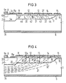
- FIG. 3 shows an alternative structural configuration of the arrangement according to FIG. 1.
- an electrically insulating layer 37 is provided here, which is grown within the semiconductor zone 3 or the semiconductor body 1 after etching out recesses 38 to 41.
- the web-shaped parts 42 to 44 of the semiconductor zone 3 remaining between the recesses 38 to 41 are contacted by the field plates 12 to 14 applied to the insulating layer 37, while the field plates 11 and 15 according to FIG. 1 contact the semiconductor region 2 and the region 16 to contact.
- the course of the equipotential lines, not shown, within the space charge zone building up at the pn junction 4a, 4b when a reverse voltage is applied corresponds to the illustration according to FIG. 1.
- the structure according to FIG. 3 is also when an n-conducting region 45 is inserted into region 2 important for bipolar transistors and, if used accordingly in FIG. 2, also for thyristors.
- Fig. 4 shows an embodiment of the invention, in which the distance of the contact holes, for example 17, from the field plate edges, for example 12a, is not constant, but varies from field plate to field plate.
- the innermost and outermost field plates 11 and 15 are formed in the same way as in Fig. 1, while the distances of the contact holes of the field plates 12 to 14 from the respective left plate edges from a relatively small value in the field plate 12 to one relatively large value increase with the field plate 14.
- the contact hole 17 is also at a clear distance from the left plate edge 12a, just like the contact hole 19 from the right plate edge of the field plate 14.
- the areas of the local doping maxima 30 ', 31' and 32 'in the p-doped semiconductor zone have different widths.
- the equipotential lines 21, 22 and the intermediate equipotential lines have approximately the same course as in FIG. 1.
- the structure according to FIG. 4 can in particular have a smaller penetration depth of the semiconductor zone 3 than the structure according to FIG. 1.
- the illustrated exemplary embodiments of the pn junction according to the invention are preferably on rotationally symmetrical semiconductor bodies, i.e. Semiconductor wafers with circular lateral boundaries, realized.
- the parts 2, 3, 33 and 45 also have circular lateral boundaries, while the field plates 11 to 15 have the shape of circular rings.
- the invention also includes those in which the semiconductor regions mentioned are in each case replaced by those of the opposite conductivity type, a voltage of the opposite sign being used instead of the voltage U mentioned.
Description
Die Erfindung bezieht sich auf einen planaren pn-Übergang hoher Spannungsfestigkeit nach dem Oberbegriff des Patentanspruchs 1.The invention relates to a planar pn junction of high dielectric strength according to the preamble of claim 1.
Ein planarer pn-Übergang dieser Art ist aus dem Jap. Journal of Appl. Physics, Vol. 21 (1982) Suppl. 21-1, S. 97-101 bekannt. Hierbei kontaktieren die Feldplatten in unmittelbarer Nähe ihrer inneren, d.h. dem Halbleitergebiet zugewandten, Ränder den Halbleiterkörper. Der Halbleiterkörper ist zusätzlich mit einer der Anzahl der Feldplatten entsprechenden Anzahl von Feldringen versehen, die aus ringförmigen Halbleiterzonen bestehen, welche denselben Leitfähigkeitstyp aufweisen wie das durch den pn-Übergang begrenzte Halbleitergebiet. Die Feldringe umgeben das Halbleitergebiet in jeweils ansteigender Entfernung vom Rand des pn-Übergangs. Jede einzelne der Feldplatten kontaktiert einen ihr zugeordneten Feldring, so daß dieser das Potential der Feldplatte bestimmt. Zwischen dem Halbleitergebiet und dem innersten Feldring sowie zwischen den einzelnen Feldringen befinden sich Teilzonen des schwach dotierten Halbleiterkörpers, die eine zum Halbleitergebiet entgegengesetzte Leitfähigkeit aufweisend und sich bis zu der den planaren pn-Übergang enthaltenden Grenzfläche erstrecken. Die Feldplatten bewirken gemeinsam mit den Feldringen, daß der pn-Übergang beim Anlegen einer ihn sperrenden Spannung, die über zwei das Halbleitergebiet und den Halbleiterkörper jeweils kontaktierende Elektroden zugeführt wird, in seinem planaren Randbereich eine hohe Durchbruchspannung aufweist. Diese Durchbruchspannung entspricht etwa seiner Volumensdurchbruchspannung, die als diejenige Spannung definiert ist, bei der der pn-Übergang in seinem parallel zur Grenzfläche des Halbleiterkörpers verlaufenden Teil, also im Volumen des Halbleiterkörpers, durchbricht.A planar pn junction of this kind is from Jap. Journal of Appl. Physics, Vol. 21 (1982) Suppl. 21-1, pp. 97-101. In this case, the field plates contact the semiconductor body in the immediate vicinity of their inner edges, ie, edges facing the semiconductor region. The semiconductor body is additionally provided with a number of field rings corresponding to the number of field plates, which consist of annular semiconductor zones which have the same conductivity type as the semiconductor region delimited by the pn junction. The field rings surround the semiconductor region at an increasing distance from the edge of the pn junction. Each one of the field plates contacts a field ring assigned to it, so that it determines the potential of the field plate. Between the semiconductor region and the innermost field ring and between the individual field rings there are subzones of the weakly doped semiconductor body, which have a conductivity opposite to the semiconductor region and extend to the interface containing the planar pn junction. Together with the field rings, the field plates cause the pn junction to have a high breakdown voltage in its planar edge region when a voltage blocking it, which is supplied via two electrodes contacting the semiconductor region and the semiconductor body, is applied. This breakdown voltage corresponds approximately to its volume breakdown voltage, which is defined as the voltage at which the pn junction breaks down in its part running parallel to the interface of the semiconductor body, that is to say in the volume of the semiconductor body.
Bei dieser bekannten pn-Struktur ist es jedoch nachteilig, daß die Feldplatten und Feldringe, die zum Erzielen einer hohen Durchbruchspannung notwendig sind, einen relativ großen Teil der an den Rand des pn-Übergangs angrenzenden Halbleiterfläche benötigen.With this known pn structure, however, it is disadvantageous that the field plates and field rings, which are necessary to achieve a high breakdown voltage, require a relatively large part of the semiconductor area adjacent to the edge of the pn junction.
Der Erfindung liegt die Aufgabe zugrunde, einen planaren pn-Übergang der eingangs genannten Art anzugeben, der für eine gewünschte hohe Durchbruchspannung auf einer wesentlich kleineren Halbleiterfläche realisiert werden kann, als das bei dem bekannten pn-Übergang der Fall ist. Das wird erfindungsgemäß durch eine Ausbildung nach dem kennzeichnenden Teil des Patentanspruchs 1, erreicht.The invention is based on the object of specifying a planar pn junction of the type mentioned at the outset which can be implemented for a desired high breakdown voltage on a substantially smaller semiconductor area than is the case with the known pn junction. This is achieved according to the invention by training according to the characterizing part of patent claim 1.
Der mit der Erfindung erzielbare Vorteil liegt insbesondere darin, daß der pn-Übergang auf einer relativ kleinen Halbleiterfläche realisierbar ist, wobei jedoch für seinen planaren Randbereich ein hoher Wert der Durchbruchspannung erreicht wird, der etwa der Volumensdurchbruchspannung entspricht. Weiterhin ist der Wert der Durchbruchspannung im Randbereich von dem Wert der Dotierungskonzentration des Halbleiterkörpers unabhängig, da die Feldplatten jeweils Teile der das Halbleitergebiet in lateraler Richtung verlängernden Halbleiterzone überdecken, die den gleichen Leitfähigkeitstyp aufweisen wie das Halbleitergebiet. Im Gegensatz hierzu überdecken die Feldplatten des oben erwähnten, bekannten pn-Übergangs Teilzonen des Halbleiterkörpers, die schwach dotiert sind und einen zum Halbleitergebiet entgegengesetzten Leitfähigkeitstyp aufweisen.The advantage that can be achieved with the invention is, in particular, that the pn junction can be implemented on a relatively small semiconductor area, but a high breakdown voltage value is achieved for its planar edge region, which corresponds approximately to the volume breakdown voltage. Furthermore, the value of the breakdown voltage in the edge region is independent of the value of the doping concentration of the semiconductor body, since the field plates each cover parts of the semiconductor zone that extend the semiconductor region in the lateral direction and have the same conductivity type as the semiconductor region. In contrast to this, the field plates of the above-mentioned known pn junction cover sub-zones of the semiconductor body which are weakly doped and have a conductivity type opposite to the semiconductor region.
Die Ansprüche 2 und 3 sind auf bevorzugte Ausgestaltungen und Weiterbildungen der Erfindung gerichtet.
Die Erfindung wird nachfolgend anhand der Zeichnung näher erläutert. Dabei zeigt:
- Fig. 1
- einen Querschnitt durch den Randbereich eines planaren pn-Übergangs nach der Erfindung,
- Fig. 2
- einen Querschnitt durch den Randbereich eines erfindungsgemäßen planaren pn-Übergangs zwischen der p-Basis und der n-Basis eines Thyristors,
- Fig. 3
- einen Querschnitt durch den Randbereich eines anderen erfindungsgemäßen planaren pn-Übergangs, und
- Fig. 4
- eine Variante des pn-Übergangs nach Fig. 1.
- Fig. 1
- 3 shows a cross section through the edge region of a planar pn junction according to the invention,
- Fig. 2
- 3 shows a cross section through the edge region of a planar pn junction according to the invention between the p base and the n base of a thyristor,
- Fig. 3
- a cross section through the edge region of another planar pn junction according to the invention, and
- Fig. 4
- a variant of the pn transition according to FIG. 1.
In Fig. 1 ist ein Halbleiterkörper 1, z.B. aus n-dotiertem Silizium mit einer Dotierungskonzentration von 10¹⁴cm⁻³ dargestellt, in den ein p-leitendes Halbleitergebiet 2 eingefügt ist. Dieses weist an der Grenzfläche 1a von 1 etwa eine Dotierungskonzentration von 10¹⁸cm⁻³ auf. Das Halbleitergebiet 2 wird in lateraler Richtung durch eine p-dotierte Halbleiterzone 3 verlängert, deren Dotierungsgrad z.B. 10¹⁶cm⁻³ beträgt und somit wesentlich niedriger ist als der des Halbleitergebiets 2. Das Halbleitergebiet 2 und die Halbleiterzone 3 werden durch einen pn-Übergang 4a, 4b vom übrigen Teil des Halbleiterkörpers 1 getrennt. Während das Teil 4a des pn-Übergangs im wesentlichen parallel zur Grenzfläche 1a des Halbleiterkörpers 1 verläuft, nähert sich das Teil 4b mit steigender Entfernung vom Rand des Halbleitergebiets 2 allmählich der Grenzfläche 1a an und erreicht diese bei 5. Die p-leitenden Teile 2 und 3 und der unterhalb des pn-Übergangs 4a, 4b liegende n-leitende Teil des Halbleiterkörpers 1 stellen z.B. eine Halbleiterdiode dar, wobei der Halbleiterkörper 1 an seiner Unterseite mit einer anodenseitigen Elektrode 6 versehen ist, die einen Anodenanschluß 7 aufweist, und das Gebiet 2 sowie die mit diesem zusammenhängende Halbleiterzone 3 von einer kathodenseitigen Elektrode 8 kontaktiert werden, die mit einem Kathodenanschluß 9 verbunden ist.In Fig. 1 a semiconductor body 1, e.g. made of n-doped silicon with a doping concentration of 10¹⁴cm⁻³, in which a p-
Die Halbleiterzone 3 kann zweckmäßigerweise nach einem Verfahren hergestellt werden, das in der EP-A-0 176 778 eingehend beschrieben ist. Ein anderes Verfahren zur Herstellung dieser Halbleiterzone kann den IEEE Transactions on Electron Devices, ED-30 (1983), S. 954 entnommen werden.The
Oberhalb der Halbleiterzone 3 wird auf der Grenzfläche 1a eine elektrisch isolierende Schicht 10 aufgebracht, die z.B. eine Schichtdicke von 10 µm aufweist. Auf der Schicht 10 sind Feldplatten 11 bis 15 aus elektrisch leitendem Material, z.B. Al oder hochdotiertem polykristallinen Silizium, angeordnet, von denen die mit 11 bezeichnete, innerste Feldplatte unmittelbar im Randbereich des Halbleitergebiets 2 liegt und dieses mit ihrem inneren Plattenrand 11a kontaktiert. Die Feldplatten 12, 13, 14 und 15 weisen in dieser Reihenfolge jeweils ansteigende Abstände vom Halbleitergebiet 2 auf, wobei die äußerste Feldplatte 15 mit ihrem rechten, also äußeren Plattenrand 15a den Halbleiterkörper 1 außerhalb des Randes 5 des pn-Übergangs 4a, 4b kontaktiert. Zweckmäßigerweise ist in den Halbleiterkörper 1 eine n-leitende Kontaktzone 16 eingefügt, die z.B. eine Dotierungskonzentration von 10¹⁸cm⁻³ aufweist und ausgehend von dem außerhalb der Begrenzung 5 des pn-Übergangs 4a, 4b liegenden Teil der Grenzfläche 1a sich geringfügig in den Halbleiterkörper hinein erstreckt. Die Feldplatte 15 kontaktiert dann die Kontaktzone 16. Die Feldplatten 12, 13 und 14 kontaktieren jeweils im Bereich von Kontaktlöchern 17, 18 und 19 die p-leitende Halbleiterzone 3. Dabei ist das Kontaktloch 17 so angeordnet, daß es gleiche Abstände vom inneren Plattenrand 12a und vom äußeren Plattenrand 12b der Feldplatte 12 hat. Auch die Kontaktlöcher 18 und 19 sind so angeordnet, daß sie von den inneren und äußeren Rändern der ihnen zugeordneten Feldplatten 13 und 14 jeweils gleiche Abstände aufweisen. Die Feldplatten 11 bis 15 sind jeweils so dicht nebeneinander angeordnet, daß sie nur schmale Spalte zwischen sich freilassen, die z.B. 10 µm betragen. Die gesamte Feldplattenanordnung 11 bis 15 kann durch eine Isolierschicht 20 abgedeckt werden, die zur Passivierung dient. Sie besteht beispielsweise aus amorphem Silizium oder Kautschuk.Above the
Legt man an den Anschluß 7 eine Spannung U hinreichender Größe, während sich der Anschluß 9 auf Massepotential befindet, so baut sich an dem in Sperrrichtung vorgespannnten pn-Übergang 4a, 4b eine Raumladungszone auf, deren unterer Rand durch die gestrichelte Linie 21 und deren oberer Rand durch die innerhalb des Gebiets 2 liegende gestrichelte Linie 22 gegeben ist. Dabei stellt 21 gleichzeitig eine Äquipotentiallinie dar, die dem Spannungswert U entspricht, während 22 eine Äquipotentiallinie bedeutet, die dem Massepotential entspricht. Die zwischen 21 und 22 befindlichen, gestrichelten Linien 23 bis 29 stellen dann jeweils weitere Äquipotentiallinien für gegeneinander abgestufte Spannungszwischenwerte dar, wobei 23 z.B. einen Potentialwert kennzeichnet, der sich nur geringfügig von U unterscheidet, während die auf der Linie 29 liegenden Punkte ein sich nur wenig vom Massepotential unterscheidendes Potential aufweisen. Die Äquipotentiallinien 29 und 28 verlaufen, wie in Fig. 1 dargestellt, durch den Spalt zwischen den Feldplatten 11 und 12, die Äquipotentiallinien 27 und 26 durch den Spalt zwischen 12 und 13 usw.. Um den an sich stark gekrümmten Verlauf der Äquipotentiallinie 28 in der Nähe der Grenzfläche 1a in einen mehr geradlinigen Verlauf umzuformen, ist die Halbleiterzone 3 unterhalb des Teiles der Feldplatte 12, der sich von dem Kontaktloch 17 zum linken Plattenrand 12a erstreckt, mit einem lokalen Dotierungsmaximum versehen, was durch eine schraffierte Fläche 30 angedeutet ist. In analoger Weise wird der Verlauf der Äquipotentiallinie 26 durch ein weiteres lokales Dotierungsmaximum 31 der Halbleiterzone 3 begradigt. Entsprechendes gilt für die Äquipotentiallinie 24, deren Verlauf durch ein lokales Dotierungsmaximum 32 der Halbleiterzone 3 beeinflußt wird.If a voltage U of sufficient magnitude is applied to the terminal 7 while the terminal 9 is at ground potential, a space charge zone is built up at the
Der Verlauf der Äquipotentiallinien 21 bis 29 zeigt, daß es auch bei großen Werten von U an der Grenzfläche 1a in Bereichen des pn-Übergangs 4b, welche zwischen den Kontaktlöchern, z.B. 17, und den linken Feldplattenrändern, z.B. 12a, liegen, die Feldgradienten nicht so groß werden, daß die Gefahr eines Durchbruchs im Silizium besteht. Die erfindungsgemäße Struktur zeichnet sich dadurch aus, daß der laterale Spannungsabfall im Bereich zwischen der Grenzfläche 1a und dem pn-Übergang 4b gleichmäßig verläuft und dementsprechend auch innerhalb der Raumladungszone 21, 22 in der Nähe der Grenzfläche 1a eine relativ gleichmäßige Feldverteilung herrscht, obwohl die links von den zugeordneten Kontaktlöchern, z.B. 17, angeordneten Feldplattenränder, z.B. 12a, an sich Störungen des gleichmäßigen Feldverlaufs hervorrufen würden. Diese Störungen werden jedoch durch die Dotierungsmaxima, z. B. 30, der Halbleiterzone 3 weitgehend kompensiert. Die lateralen Maxima der Dotierungskonzentration, die etwa innerhalb der schraffierten Bereiche 30, 31 und 32 der Halbleiterzone 3 vorhanden sind, können z.B. um den Faktor 10 höher sein als die Werte der Dotierungskonzentration in den hieran angrenzenden Teilen der Zone 3. Die großflächige Abdeckung des Randbereiches des pn-Übergangs 4a, 4b durch die Feldplatten 11 bis 15, die nur schmale Spalte zwischen sich freilassen, bewirkt, daß die mit der erfindungsgemäßen Struktur erzielbare hohe Durchbruchspannung auch durch den Einfluß von z.B. wasserhaltigen Materialien, die zur Passivierung benutzt werden, nicht reduziert wird.The course of the equipotential lines 21 to 29 shows that even with large values of U at the
Die pn-Struktur nach Fig. 1 ist beispielsweise auch für vertikale bipolare Leistungstransistoren von Bedeutung. Einen solchen Transistor erhält man, wenn man ein n-leitendes Halbleitergebiet 33 so in das p-Halbleitergebiet 2 einfügt, daß es durch einen weiteren pn-Übergang 34 von diesem getrennt ist. 33 bezeichnet dann das Emittergebiet, 2 und 3 das Basisgebiet und 1 das Kollektorgebiet des Transistors. Die Elektroden 6 und 8 stellen die Kollektor- und Emitterelektrode dar, 7 und 9 den Kollektor- und Emitteranschluß. Das Basisgebiet 2 ist mit einer nicht dargestellten Basiselektrode versehen, die einen Anschluß für einen Basisstromkreis aufweist. Die mit der Erfindung erreichbare hohe Durchbruchspannung am Basis-Kollektor-Übergang 4a, 4b bewirkt eine hohe Spannungsfestigkeit dieses Transistors.The pn structure according to FIG. 1 is also important for vertical bipolar power transistors, for example. Such a transistor is obtained if an n-
Fig. 2 zeigt die Anwendung der pn-Struktur nach Fig. 1 auf einen Thyristor. Das Gebiet 33 stellt hierbei den n-Emitter dar, das Gebiet 2 einschließlich der Zone 3 die p-Basis, der unterhalb von 4a und 4b liegende Teil des Halbleiterkörpers 1 die n-Basis und eine zusätzliche, p-dotierte Halbleiterschicht 35 an der Unterseite von 1 den p-Emitter des Thyristors. Die Elektrode 8 bedeutet die kathodenseitige Elektrode und eine die Schicht 35 kontaktierende Elektrode 36 die anodenseitige Elektrode des Thyristors. Die Anschlüsse von 8 und 36 werden hier mit K und A bezeichnet. Eine nicht dargestellte, das Gebiet 2 kontaktierende Elektrode bildet die Gateelektrode des Thyristors, die zum Zünden und/oder zum Löschen desselben mit Zünd- oder Löschsignalen beaufschlagt wird.FIG. 2 shows the application of the pn structure according to FIG. 1 to a thyristor. The
In Fig. 3 ist eine alternative strukturelle Ausgestaltung der Anordnung nach Fig. 1 dargestellt. Dabei sind die bereits anhand von Fig. 1 beschriebenen Strukturteile mit denselben Bezugszeichen versehen. Zum Unterschied von Fig. 1 ist hier eine elektrisch isolierende Schicht 37 vorgesehen, die nach dem Ausätzen von Ausnehmungen 38 bis 41 aus der Halbleiterzone 3 bzw. dem Halbleiterkörper 1 innerhalb derselben aufgewachsen wird. Die jeweils zwischen den Ausnehmungen 38 bis 41 verbleibenden, stegförmigen Teile 42 bis 44 der Halbleiterzone 3 werden von den auf die isolierende Schicht 37 aufgebrachten Feldplatten 12 bis 14 kontaktiert, während die Feldplatten 11 und 15 entsprechend Fig. 1 das Halbleitergebiet 2 und das Gebiet 16 kontaktieren. Der nicht gezeigte Verlauf der Äquipotentiallinien innerhalb der sich am pn-Übergang 4a, 4b beim Anlegen einer Sperrspannung aufbauenden Raumladungszone entspricht der Darstellung nach Fig. 1. Die Struktur nach Fig. 3 ist bei Einfügung eines n-leitenden Gebiets 45 in das Gebiet 2 auch für bipolare Transistoren von Bedeutung und bei entsprechender Anwendung auf Fig. 2 auch für Thyristoren.FIG. 3 shows an alternative structural configuration of the arrangement according to FIG. 1. The structural parts already described with reference to FIG. 1 are provided with the same reference symbols. In contrast to FIG. 1, an electrically insulating
Fig. 4 zeigt ein Ausführungsbeispiel der Erfindung, bei dem der Abstand der Kontaktlöcher, z.B. 17, von den Feldplattenrändern, z.B. 12a, nicht konstant ist, sondern von Feldplatte zu Feldplatte variiert. Im einzelnen sind die innerste und die äußerste Feldplatte 11 bzw. 15 in gleicher Weise ausgebildet wie in Fig. 1, während die Abstände der Kontaktlöcher der Feldplatten 12 bis 14 von den jeweiligen linken Plattenrändern von einem relativ kleinen Wert bei der Feldplatte 12 bis zu einem relativ großen Wert bei der Feldplatte 14 ansteigen. Das Kontaktloch 17 weist jedoch auch hier einen deutlichen Abstand vom linken Plattenrand 12a auf, ebenso wie das Kontaktloch 19 vom rechten Plattenrand der Feldplatte 14. Entsprechend den unterschiedlichen Längen der sich jeweils links von den zugeordneten Kontaktlöchern befindenden Plattenteile weisen die Bereiche der lokalen Dotierungsmaxima 30′, 31′ und 32′ in der p-dotierten Halbleiterzone unterschiedliche Breiten auf. Die Äquipotentiallinien 21, 22 und die dazwischenliegenden Äquipotentiallinien haben etwa den gleichen Verlauf wie in Fig. 1. Die Struktur nach Fig. 4 kann insbesondere eine kleinere Eindringtiefe der Halbleiterzone 3 aufweisen als die Struktur nach Fig. 1.Fig. 4 shows an embodiment of the invention, in which the distance of the contact holes, for example 17, from the field plate edges, for example 12a, is not constant, but varies from field plate to field plate. Specifically, the innermost and
Die dargestellten Ausführungsbeispiele des pn-Übergangs nach der Erfindung sind vorzugsweise auf rotationssymmetrischen Halbleiterkörpern, d.h. Halbleiterscheiben mit kreisförmigen lateralen Begrenzungen, realisiert. Dabei weisen auch die Teile 2, 3, 33 und 45 kreisförmige laterale Begrenzungen auf, während die Feldplatten 11 bis 15 die Form von Kreisringen haben.The illustrated exemplary embodiments of the pn junction according to the invention are preferably on rotationally symmetrical semiconductor bodies, i.e. Semiconductor wafers with circular lateral boundaries, realized. The
Neben den bisher beschriebenen Ausführungsformen gehören auch solche zur Erfindung, bei denen die genannten Halbleitergebiete jeweils durch solche des entgegengesetzten Leitfähigkeitstyps ersetzt sind, wobei anstelle der genannten Spannung U eine Spannung des entgegengesetzten Vorzeichens verwendet wird.In addition to the embodiments described so far, the invention also includes those in which the semiconductor regions mentioned are in each case replaced by those of the opposite conductivity type, a voltage of the opposite sign being used instead of the voltage U mentioned.
Claims (3)
- Planar p-n junction (4a, 4b) which has high voltage sustaining capability and which extends essentially parallel to the boundary surface (1a) of a doped semiconductor body (1) of a first conductivity type and separates a semiconductor region (2), inserted in said semiconductor body (1), of a second conductivity type from the rest of the semiconductor body (1), a plurality of field plates (11 to 15) which are separated by an electrically isolating layer (10) from the boundary surface (1a) and contact the semiconductor body in each case in the region of a via (17 to 19) in said layer (10) being provided in the peripheral region of the semiconductor region (2), characterized in that, at least in the case of some of the field plates (12 to 14) with the exception of the innermost (11) and the outermost (15), the vias (17) are arranged so that in each case they are at a distance from the inner field-plate periphery (12a), which distance is equal to, falls below or exceeds their distance from the outer field-plate periphery (12b), the degree to which it falls below or exceeds only being large enough for the vias (17) still to be at a perceptible distance from the inner field-plate periphery (12a) and outer field-plate periphery (12b), in that the semiconductor region (2) is extended in the lateral direction by a semiconductor zone (3) which is situated underneath the field plates (11 to 15), is of the second conductivity type and has planar peripheral termination and whose degree of doping is substantially less than that of the semiconductor region (2), and in that the degree of doping of the semiconductor zone (3) varies in its magnitude in the lateral direction, having in each case local maxima (30) underneath the field-plate components which are situated between the vias (17) and the field plates (12) associated with the inner peripheries (12a).
- Planar p-n junction according to Claim 1, characterized in that the electrically insulating layer (37) comprises a plurality of sublayers which are provided in a plurality of superficial recesses (38 to 41) of the semiconductor zone (3), in that there is present, between each two mutually adjacent recesses (38, 39) of this type, a fillet (42) of the semiconductor zone (3), which fillet extends up to the boundary surface (1a) and serves to contact a field plate (12) which is deposited on the sublayers situated in the two adjacent recesses (38, 39), and in that the peripheries, adjacent to the fillet (42) of the sublayers which are provided in the adjacent recesses (38, 39) form the boundary between them of the via allocated to said field plate (12).
- Planar p-n junction according to Claim 1 or 2, characterized in that the distances of the vias (17) from the inner field-plate peripheries (12a) of the field plates (12) allocated to them in each case increase with increasing distance of the field plates (12) from the periphery of the semiconductor region (2).
Applications Claiming Priority (2)
| Application Number | Priority Date | Filing Date | Title |
|---|---|---|---|
| DE3831941 | 1988-09-20 | ||
| DE3831941 | 1988-09-20 |
Publications (3)
| Publication Number | Publication Date |
|---|---|
| EP0360036A2 EP0360036A2 (en) | 1990-03-28 |
| EP0360036A3 EP0360036A3 (en) | 1990-05-30 |
| EP0360036B1 true EP0360036B1 (en) | 1994-06-01 |
Family
ID=6363338
Family Applications (1)
| Application Number | Title | Priority Date | Filing Date |
|---|---|---|---|
| EP89115841A Expired - Lifetime EP0360036B1 (en) | 1988-09-20 | 1989-08-28 | Planar pn-junction having a high withstand voltage |
Country Status (4)
| Country | Link |
|---|---|
| US (1) | US5113237A (en) |
| EP (1) | EP0360036B1 (en) |
| JP (1) | JP2974696B2 (en) |
| DE (1) | DE58907758D1 (en) |
Cited By (1)
| Publication number | Priority date | Publication date | Assignee | Title |
|---|---|---|---|---|
| DE102008032711B4 (en) | 2007-07-12 | 2019-01-03 | Fuji Electric Co., Ltd. | Semiconductor device |
Families Citing this family (39)
| Publication number | Priority date | Publication date | Assignee | Title |
|---|---|---|---|---|
| JP2850694B2 (en) * | 1993-03-10 | 1999-01-27 | 株式会社日立製作所 | High breakdown voltage planar type semiconductor device |
| US5959342A (en) * | 1993-12-08 | 1999-09-28 | Lucent Technologies Inc. | Semiconductor device having a high voltage termination improvement |
| US5381031A (en) * | 1993-12-22 | 1995-01-10 | At&T Corp. | Semiconductor device with reduced high voltage termination area and high breakdown voltage |
| US5486718A (en) * | 1994-07-05 | 1996-01-23 | Motorola, Inc. | High voltage planar edge termination structure and method of making same |
| JP3581447B2 (en) * | 1995-08-22 | 2004-10-27 | 三菱電機株式会社 | High voltage semiconductor device |
| US5801836A (en) * | 1996-07-16 | 1998-09-01 | Abb Research Ltd. | Depletion region stopper for PN junction in silicon carbide |
| DE19843659A1 (en) * | 1998-09-23 | 2000-04-06 | Siemens Ag | Semiconductor component with a structured semiconductor body |
| WO2000038242A1 (en) * | 1998-12-18 | 2000-06-29 | Infineon Technologies Ag | Power semiconductor element |
| DE10051909B4 (en) * | 2000-10-19 | 2007-03-22 | Infineon Technologies Ag | Edge termination for high-voltage semiconductor component and method for producing an isolation trench in a semiconductor body for such edge termination |
| US6563197B1 (en) * | 2001-11-20 | 2003-05-13 | International Rectifier Corporation | MOSgated device termination with guard rings under field plate |
| JP4326835B2 (en) * | 2003-05-20 | 2009-09-09 | 三菱電機株式会社 | Semiconductor device, semiconductor device manufacturing method, and semiconductor device manufacturing process evaluation method |
| US7394158B2 (en) * | 2004-10-21 | 2008-07-01 | Siliconix Technology C.V. | Solderable top metal for SiC device |
| US7812441B2 (en) | 2004-10-21 | 2010-10-12 | Siliconix Technology C.V. | Schottky diode with improved surge capability |
| US7834376B2 (en) * | 2005-03-04 | 2010-11-16 | Siliconix Technology C. V. | Power semiconductor switch |
| US9419092B2 (en) * | 2005-03-04 | 2016-08-16 | Vishay-Siliconix | Termination for SiC trench devices |
| US7955345B2 (en) * | 2005-04-01 | 2011-06-07 | Nexgen Medical Systems, Inc. | Thrombus removal system and process |
| US20060255401A1 (en) * | 2005-05-11 | 2006-11-16 | Yang Robert K | Increasing breakdown voltage in semiconductor devices with vertical series capacitive structures |
| DE102005023668B3 (en) * | 2005-05-23 | 2006-11-09 | Infineon Technologies Ag | Semiconductor component e.g. metal oxide semiconductor field effect transistor (MOSFET) has middle region surrounded by boundary region whose straight line section has smaller breakdown voltage than curved edge section |
| US7550787B2 (en) * | 2005-05-31 | 2009-06-23 | International Business Machines Corporation | Varied impurity profile region formation for varying breakdown voltage of devices |
| US20070012983A1 (en) * | 2005-07-15 | 2007-01-18 | Yang Robert K | Terminations for semiconductor devices with floating vertical series capacitive structures |
| US8368165B2 (en) * | 2005-10-20 | 2013-02-05 | Siliconix Technology C. V. | Silicon carbide Schottky diode |
| CN101506989B (en) * | 2006-07-31 | 2014-02-19 | 威世-硅尼克斯 | Molybdenum barrier metal for sic schottky diode and process of manufacture |
| US20090189240A1 (en) * | 2008-01-25 | 2009-07-30 | Infineon Technologies Austria Ag | Semiconductor device with at least one field plate |
| CN101414634B (en) * | 2008-12-01 | 2010-06-02 | 西安电子科技大学 | Heterojunction field effect transistor for groove insulated gate type multiple source field plate |
| US8410549B2 (en) * | 2009-03-27 | 2013-04-02 | National Semiconductor Corporation | Structure and fabrication of field-effect transistor using empty well in combination with source/drain extensions or/and halo pocket |
| US8163619B2 (en) * | 2009-03-27 | 2012-04-24 | National Semiconductor Corporation | Fabrication of semiconductor structure having asymmetric field-effect transistor with tailored pocket portion along source/drain zone |
| US8084827B2 (en) * | 2009-03-27 | 2011-12-27 | National Semiconductor Corporation | Structure and fabrication of like-polarity field-effect transistors having different configurations of source/drain extensions, halo pockets, and gate dielectric thicknesses |
| US7968921B2 (en) * | 2009-03-27 | 2011-06-28 | National Semiconductor Corporation | Asymmetric field-effect transistor having asymmetric channel zone and differently configured source/drain extensions |
| US7973372B2 (en) * | 2009-03-27 | 2011-07-05 | National Semiconductor Corporation | Semiconductor structure in which source and drain extensions of field-effect transistor are defined with different dopants |
| US20100244151A1 (en) * | 2009-03-27 | 2010-09-30 | National Semiconductor Corporation | Structure and fabrication of field-effect transistor having source/drain extension defined by multiple local concentration maxima |
| JP5515922B2 (en) | 2010-03-24 | 2014-06-11 | 富士電機株式会社 | Semiconductor device |
| US8716717B2 (en) | 2010-10-15 | 2014-05-06 | Mitsubishi Electric Corporation | Semiconductor device and method for manufacturing the same |
| US9614043B2 (en) | 2012-02-09 | 2017-04-04 | Vishay-Siliconix | MOSFET termination trench |
| US9842911B2 (en) | 2012-05-30 | 2017-12-12 | Vishay-Siliconix | Adaptive charge balanced edge termination |
| JP6020317B2 (en) | 2013-04-05 | 2016-11-02 | 三菱電機株式会社 | Semiconductor element |
| JP2014204038A (en) * | 2013-04-08 | 2014-10-27 | 三菱電機株式会社 | Semiconductor device and manufacturing method of the same |
| US9887259B2 (en) | 2014-06-23 | 2018-02-06 | Vishay-Siliconix | Modulated super junction power MOSFET devices |
| EP3183754A4 (en) | 2014-08-19 | 2018-05-02 | Vishay-Siliconix | Super-junction metal oxide semiconductor field effect transistor |
| DE102016120301A1 (en) * | 2016-10-25 | 2018-04-26 | Infineon Technologies Ag | Power semiconductor device termination structure |
Family Cites Families (22)
| Publication number | Priority date | Publication date | Assignee | Title |
|---|---|---|---|---|
| NL6904619A (en) * | 1969-03-25 | 1970-09-29 | ||
| DE1920397A1 (en) * | 1969-04-22 | 1970-11-12 | Siemens Ag | Stabilized semiconductor component |
| DE2241600A1 (en) * | 1971-08-26 | 1973-03-01 | Dionics Inc | HIGH VOLTAGE P-N TRANSITION AND ITS APPLICATION IN SEMICONDUCTOR SWITCHING ELEMENTS, AND THE PROCESS FOR ITS MANUFACTURING |
| JPS523277B2 (en) * | 1973-05-19 | 1977-01-27 | ||
| US4079403A (en) * | 1976-11-01 | 1978-03-14 | Electric Power Research Institute, Inc. | Thyristor device with self-protection against breakover turn-on failure |
| DE2846637A1 (en) * | 1978-10-11 | 1980-04-30 | Bbc Brown Boveri & Cie | SEMICONDUCTOR COMPONENT WITH AT LEAST ONE PLANAR PN JUNCTION AND ZONE GUARD RINGS |
| DE3117804A1 (en) * | 1981-05-06 | 1982-11-25 | Robert Bosch Gmbh, 7000 Stuttgart | "PLANAR TRANSISTOR STRUCTURE" |
| DE3201545A1 (en) * | 1982-01-20 | 1983-07-28 | Robert Bosch Gmbh, 7000 Stuttgart | PLANAR SEMICONDUCTOR ARRANGEMENT |
| JPS5976466A (en) * | 1982-10-25 | 1984-05-01 | Mitsubishi Electric Corp | Planar type semiconductor device |
| NL8204105A (en) * | 1982-10-25 | 1984-05-16 | Philips Nv | SEMICONDUCTOR DEVICE. |
| GB2131603B (en) * | 1982-12-03 | 1985-12-18 | Philips Electronic Associated | Semiconductor devices |
| GB2134705B (en) * | 1983-01-28 | 1985-12-24 | Philips Electronic Associated | Semiconductor devices |
| JPS60124865A (en) * | 1983-12-09 | 1985-07-03 | Nec Corp | Semiconductor device |
| NL8401983A (en) * | 1984-06-22 | 1986-01-16 | Philips Nv | Semiconductor device with increased breakdown voltage. |
| EP0176778B1 (en) * | 1984-09-28 | 1991-01-16 | Siemens Aktiengesellschaft | Method of producing a pu junction with a high disruptive breakdown voltage |
| GB2167229B (en) * | 1984-11-21 | 1988-07-20 | Philips Electronic Associated | Semiconductor devices |
| JPS61135158A (en) * | 1984-12-06 | 1986-06-23 | Nec Corp | High withstanding-voltage semiconductor device |
| IT1202311B (en) * | 1985-12-11 | 1989-02-02 | Sgs Microelettronica Spa | SEMICONDUCTOR DEVICE WITH A FLAT JUNCTION WITH SELF-PASSIVATING TERMINATION |
| US4799100A (en) * | 1987-02-17 | 1989-01-17 | Siliconix Incorporated | Method and apparatus for increasing breakdown of a planar junction |
| GB2205682A (en) * | 1987-06-03 | 1988-12-14 | Philips Electronic Associated | A semiconductor device |
| EP0310836A3 (en) * | 1987-10-08 | 1989-06-14 | Siemens Aktiengesellschaft | Semiconductor element with a planar p-n junction |
| US4903086A (en) * | 1988-01-19 | 1990-02-20 | E-Systems, Inc. | Varactor tuning diode with inversion layer |
-
1989
- 1989-08-28 DE DE58907758T patent/DE58907758D1/en not_active Expired - Fee Related
- 1989-08-28 EP EP89115841A patent/EP0360036B1/en not_active Expired - Lifetime
- 1989-09-13 JP JP1239750A patent/JP2974696B2/en not_active Expired - Fee Related
-
1991
- 1991-05-06 US US07/698,332 patent/US5113237A/en not_active Expired - Lifetime
Cited By (1)
| Publication number | Priority date | Publication date | Assignee | Title |
|---|---|---|---|---|
| DE102008032711B4 (en) | 2007-07-12 | 2019-01-03 | Fuji Electric Co., Ltd. | Semiconductor device |
Also Published As
| Publication number | Publication date |
|---|---|
| JPH02114646A (en) | 1990-04-26 |
| JP2974696B2 (en) | 1999-11-10 |
| DE58907758D1 (en) | 1994-07-07 |
| EP0360036A2 (en) | 1990-03-28 |
| US5113237A (en) | 1992-05-12 |
| EP0360036A3 (en) | 1990-05-30 |
Similar Documents
| Publication | Publication Date | Title |
|---|---|---|
| EP0360036B1 (en) | Planar pn-junction having a high withstand voltage | |
| EP0200863B1 (en) | Semiconductor device with structures of thyristors and diodes | |
| DE19701189B4 (en) | Semiconductor device | |
| CH638928A5 (en) | SEMICONDUCTOR ARRANGEMENT. | |
| DE19811297A1 (en) | Avalanche breakdown resistant MOS devices | |
| DE112019003790T5 (en) | SUPERJUNCTION SILICON CARBIDE SEMICONDUCTOR DEVICE AND METHOD OF MANUFACTURING A SUPERJUNCTION SILICON CARBIDE SEMICONDUCTOR DEVICE | |
| DE19813509A1 (en) | Thyristor with isolated gate | |
| DE3131727A1 (en) | "MOS FIELD EFFECT TRANSISTOR AND METHOD FOR ITS PRODUCTION" | |
| EP0913000B1 (en) | Field effect controllable semiconductor component | |
| EP0477594B1 (en) | Turn-off thyristor | |
| DE19917994A1 (en) | Insulation structure for semiconductor component, e.g. bipolar transistor | |
| EP1092238A1 (en) | Universal semiconductor wafer for high-voltage semiconductor components | |
| DE4310606C2 (en) | GTO thyristors | |
| EP0332955A2 (en) | Thyristor having a large forward and reverse blocking capability, and method of making the same | |
| DE3723150C2 (en) | ||
| DE102016120301A1 (en) | Power semiconductor device termination structure | |
| EP0710988B1 (en) | Manufacturing method for semiconductor devices controlled by field effect | |
| EP0249122B1 (en) | Turn-off power semiconductor device | |
| EP0768717A2 (en) | Power semiconductor device | |
| EP0419898B1 (en) | Method of enhancing the withstand voltage of a multilayered semiconductor device | |
| DE102004005084B4 (en) | Semiconductor device | |
| DE2425364A1 (en) | GATE-CONTROLLED SEMI-CONDUCTOR RECTIFIER | |
| EP0285923B1 (en) | Gate turn-off thyristor and method of making the same | |
| EP0389942B1 (en) | High blocking voltage semiconductor device | |
| EP0206350A2 (en) | Thyristor with a reduced base thickness |
Legal Events
| Date | Code | Title | Description |
|---|---|---|---|
| PUAI | Public reference made under article 153(3) epc to a published international application that has entered the european phase |
Free format text: ORIGINAL CODE: 0009012 |
|
| AK | Designated contracting states |
Kind code of ref document: A2 Designated state(s): CH DE GB LI SE |
|
| PUAL | Search report despatched |
Free format text: ORIGINAL CODE: 0009013 |
|
| AK | Designated contracting states |
Kind code of ref document: A3 Designated state(s): CH DE GB LI SE |
|
| 17P | Request for examination filed |
Effective date: 19901127 |
|
| 17Q | First examination report despatched |
Effective date: 19930806 |
|
| GRAA | (expected) grant |
Free format text: ORIGINAL CODE: 0009210 |
|
| AK | Designated contracting states |
Kind code of ref document: B1 Designated state(s): CH DE GB LI SE |
|
| REF | Corresponds to: |
Ref document number: 58907758 Country of ref document: DE Date of ref document: 19940707 |
|
| GBT | Gb: translation of ep patent filed (gb section 77(6)(a)/1977) |
Effective date: 19940811 |
|
| EAL | Se: european patent in force in sweden |
Ref document number: 89115841.2 |
|
| PLBE | No opposition filed within time limit |
Free format text: ORIGINAL CODE: 0009261 |
|
| STAA | Information on the status of an ep patent application or granted ep patent |
Free format text: STATUS: NO OPPOSITION FILED WITHIN TIME LIMIT |
|
| 26N | No opposition filed | ||
| PGFP | Annual fee paid to national office [announced via postgrant information from national office to epo] |
Ref country code: SE Payment date: 20010829 Year of fee payment: 13 |
|
| PGFP | Annual fee paid to national office [announced via postgrant information from national office to epo] |
Ref country code: CH Payment date: 20011112 Year of fee payment: 13 |
|
| REG | Reference to a national code |
Ref country code: GB Ref legal event code: IF02 |
|
| PG25 | Lapsed in a contracting state [announced via postgrant information from national office to epo] |
Ref country code: SE Free format text: LAPSE BECAUSE OF NON-PAYMENT OF DUE FEES Effective date: 20020829 |
|
| PG25 | Lapsed in a contracting state [announced via postgrant information from national office to epo] |
Ref country code: CH Free format text: LAPSE BECAUSE OF NON-PAYMENT OF DUE FEES Effective date: 20020831 Ref country code: LI Free format text: LAPSE BECAUSE OF NON-PAYMENT OF DUE FEES Effective date: 20020831 |
|
| EUG | Se: european patent has lapsed | ||
| REG | Reference to a national code |
Ref country code: CH Ref legal event code: PL |
|
| PGFP | Annual fee paid to national office [announced via postgrant information from national office to epo] |
Ref country code: GB Payment date: 20050816 Year of fee payment: 17 |
|
| GBPC | Gb: european patent ceased through non-payment of renewal fee |
Effective date: 20060828 |
|
| PG25 | Lapsed in a contracting state [announced via postgrant information from national office to epo] |
Ref country code: GB Free format text: LAPSE BECAUSE OF NON-PAYMENT OF DUE FEES Effective date: 20060828 |
|
| PGFP | Annual fee paid to national office [announced via postgrant information from national office to epo] |
Ref country code: DE Payment date: 20071011 Year of fee payment: 19 |
|
| PG25 | Lapsed in a contracting state [announced via postgrant information from national office to epo] |
Ref country code: DE Free format text: LAPSE BECAUSE OF NON-PAYMENT OF DUE FEES Effective date: 20090303 |