EP0356597B1 - Improvement to digital filter sampling rate conversion method and device - Google Patents
Improvement to digital filter sampling rate conversion method and device Download PDFInfo
- Publication number
- EP0356597B1 EP0356597B1 EP88480021A EP88480021A EP0356597B1 EP 0356597 B1 EP0356597 B1 EP 0356597B1 EP 88480021 A EP88480021 A EP 88480021A EP 88480021 A EP88480021 A EP 88480021A EP 0356597 B1 EP0356597 B1 EP 0356597B1
- Authority
- EP
- European Patent Office
- Prior art keywords
- rate
- filter
- coefficients
- input
- samples
- Prior art date
- Legal status (The legal status is an assumption and is not a legal conclusion. Google has not performed a legal analysis and makes no representation as to the accuracy of the status listed.)
- Expired - Lifetime
Links
Images
Classifications
-
- H—ELECTRICITY
- H03—ELECTRONIC CIRCUITRY
- H03H—IMPEDANCE NETWORKS, e.g. RESONANT CIRCUITS; RESONATORS
- H03H17/00—Networks using digital techniques
- H03H17/02—Frequency selective networks
- H03H17/06—Non-recursive filters
- H03H17/0621—Non-recursive filters with input-sampling frequency and output-delivery frequency which differ, e.g. extrapolation; Anti-aliasing
- H03H17/0635—Non-recursive filters with input-sampling frequency and output-delivery frequency which differ, e.g. extrapolation; Anti-aliasing characterized by the ratio between the input-sampling and output-delivery frequencies
- H03H17/0685—Non-recursive filters with input-sampling frequency and output-delivery frequency which differ, e.g. extrapolation; Anti-aliasing characterized by the ratio between the input-sampling and output-delivery frequencies the ratio being rational
Definitions
- This invention deals with digital signal processing.
- This invention deals more particularly with a method and device for digitally converting signal sampling rate from one given rate to another given rate.
- sampling rates In many applications, one has to switch from one sampling rate to another in the course of the process. Assuming the rates are multiples to one another, up sampling may be achieved by interpolating in between consecutive samples, while down sampling would simply require regularly dropping samples. This process does not directly apply to systems wherein sampling rates ratio would not be an integer value or in other words the sampling rates would be relatively prime.
- One object of this invention is to provide a means for converting a sampled signal from one sampling rate to another within one single process.
- Another object is to provide a digital filter fed with input samples at a first rate and providing output samples at a second rate, by computing said output samples through permutations of filter coefficients sets in a predetermined order.
- the invention is set out in Claims 1 and 3.
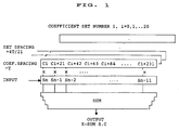
- FIGS 1 and 3 are block diagrams of filters made according to the invention.
- Figure 2 is a flow chart of the filtering process operated with the device of figure 1.
- a 19.2 Kbits/s modem is to operate at a symbol rate (baud rate) of 2742.85 symbols/s for transmitting and receiving 7 bits per symbol.
- Each symbol is selected within an (X,Y) represented constellation, and therefore is defined by two cartesian components an and bn.
- Said filter is a complex filter, but one may show that the system is fully defined by the real component r(t).
- the filter output is converted into analog form in a D/A converter and then filtered in a low cost analog low-pass filter prior to being fed to the transmission line.
- the D/A clock should be rated at 16457.1 Hz.
- a much improved solution to this rate conversion is proposed here, which, instead of focusing over the samples, focuses over the system transfer function. It combines both filtering and interpolation operations into one single operation, i.e. multi rate filtering or interpolating filtering.
- Optimal solution is provided by selecting said multiple to be equal to their lowest common multiple, i.e.
- the symbol cells are provided with taps connected to multipliers (not shown), the second inputs of which is assigned a filter coefficient (i.e. filter impulse response sample, according to digital filtering theory). Said coefficients are spaced by T/21 over the impulse response and divided into 21 sets of 12 coefficients. The spacing between the subsequent sets is 4T/21 and corresponds to the output rate.
- the coefficient sets are used sequentially. They may be stored in a memory and fetched out when needed.
- the filter output sample X is computed according to the flow diagram of Figure 2.
- i 0 and the first set of coefficients, i.e. Set(0) is fetched out of the storage (not shown).
- X(n+2) C8.Sn + C29.Sn-1 + ...
- i old + b a . k + i new i being the previous coefficient set index
- the above operation provides the number of shifts "k” to be applied to the shift register contents and the new set index (inew) for computing the new output sample.
- the filter input samples are fed into the filter shift register at their own incoming rate, while the output samples are computed by switching the filter coefficient sets at the required output rate.
- the filter coefficients are obtained by sampling the desired filter impulse response.
- a slightly less precise result may be achieved by performing interpolation operations over the coefficients of a filter originally designed to operate at rate 16457, i.e. coefficients deriving from a filter impulse response sampled at rate 6/T.
- the rationale of this invention may be extended to apply to the modem receiver filter.
- the input samples derived from the received signal are fed into a receive (Hilbert) filter delay line at the rate of 21 samples per 4T which corresponds to a sampling frequency of 14400 Hz.
- the receive filter issues two complex symbols per time T (or 8 per 4T) which are then fed into a T/2-spaced equalizer delay line.
- the filter impulse response is sampled at a rate corresponding to the lowest common multiple of twice the symbol rate (2/T) and the A/D sampling frequency.
- the delay line contents is shifted by a number of samples given by the quotient of the division of the new index by 8.
- Old set number+21 (8 . number of shifts)+New set Number
- the new set reference number should equal to n and the number of shifts equals to k.
- the filter provides eight output samples using the eight sets of coefficients Set(0) through Set(7) in a fixed order defined by the above equation.
Description
- This invention deals with digital signal processing.
- This invention deals more particularly with a method and device for digitally converting signal sampling rate from one given rate to another given rate.
- Conventional digital signal processing is achieved by sampling said signal, converting said samples into digital values and then performing mathematical operations over said digital values to achieve the desired processing.
- In many applications, one has to switch from one sampling rate to another in the course of the process. Assuming the rates are multiples to one another, up sampling may be achieved by interpolating in between consecutive samples, while down sampling would simply require regularly dropping samples. This process does not directly apply to systems wherein sampling rates ratio would not be an integer value or in other words the sampling rates would be relatively prime.
- On the other hand, an article by T.A. Ramstad: "Digital Methods for Conversion between Arbitrary Sampling Frequencies", published in IEEE Transactions on Acoustics, Speech and Signal Processing, vol. ASSP-32, no. 3, June 1984, pp 577 - 591, discusses in a rather general way possibilities for sampling rate conversion. The author acknowledging therein that for irrational rates ratio, "there will exist no periodic relation between the (filter) coefficients", proposes then to calculate new coefficients for each output sample.
- Another, rather straightforward solution would be achieved by converting the sampled signal back into the analog form and resampling it at proper rate. This solution would not only lack efficiency from a processing load standpoint, it might add to the coding error.
- Another method is disclosed in USP 4,460,890 wherein direct digital to digital conversion from a first sampling rate to a second sampling rate , not multiple to each other, is achieved using a rate multiplication means feeding an interpolating means.
- This solution is still considered rather complex and not cost optimized.
- One object of this invention is to provide a means for converting a sampled signal from one sampling rate to another within one single process.
- Another object is to provide a digital filter fed with input samples at a first rate and providing output samples at a second rate, by computing said output samples through permutations of filter coefficients sets in a predetermined order.
- The invention is set out in
Claims - Further objects, characteristics and advantages of the present invention will be explained in more details in the following description with reference to the enclosed drawings which represent a preferred embodiment thereof.
- Figures 1 and 3 are block diagrams of filters made according to the invention.
- Figure 2 is a flow chart of the filtering process operated with the device of figure 1.
- Even though the invention applies to any digital system wherein conversion is to be achieved between input and output sampling rates, the detailed description is given therein with reference to QAM-based digital modems and more particularly to digital filtering used within said modems. For details on said modems, one may refer to:
- A. Croisier and J.M. Pierret, "The Digital Echo Modulation", IEEE trans. Communication Technology, COM-18, pp 367-376 (1970).
- D. Godard and D. Pilost, "A 2400-Bits/s Microprocessor-Based Modem", IBM journal of Research and Development, Vol. 25, No.1, January 1981, pp 17-24.
- More particularly, assume a 19.2 Kbits/s modem is to operate at a symbol rate (baud rate) of 2742.85 symbols/s for transmitting and receiving 7 bits per symbol.
- Each symbol is selected within an (X,Y) represented constellation, and therefore is defined by two cartesian components an and bn. Conventional QAM modulation operations involve carrier modulating (= rotating) the symbol, then convolving (filtering) each selected and modulated symbol by a so called signal element impulse response. Said filter is a complex filter, but one may show that the system is fully defined by the real component r(t).
- For a modem operating at the 2472.85 symbols/s rate and assuming the filter impulse response be defined by six samples (coefficients) per baud time, then the filter clock should have a rate of 6 x 2742.85 = 16457.1 Hz.
- According to the conventional modem practice, the filter output is converted into analog form in a D/A converter and then filtered in a low cost analog low-pass filter prior to being fed to the transmission line. Naturally, the D/A clock should be rated at 16457.1 Hz.
- But assuming one wishes to use a D/A converter clocked at 14400 Hz, the filter output signal S(t) would need being resampled properly. Since 14400 and 16457 Hz or 2742.85 Hz are not multiple to each other, the sampling rate conversion operation cannot be achieved in a straightforward manner.
- One may interpolate input samples to achieve the rate conversion. But not only this solution means additional computing load which might affect the modem signal processor efficiency, it also affects the process precision by adding interpolation noise.
- A much improved solution to this rate conversion is proposed here, which, instead of focusing over the samples, focuses over the system transfer function. It combines both filtering and interpolation operations into one single operation, i.e. multi rate filtering or interpolating filtering. To that end, the filter impulse response h(t) is sampled at a rate higher than it should normally be; rate multiple of the symbols rate (A = 2742.85) and the D/A converter clock rate (B = 14 400). Optimal solution is provided by selecting said multiple to be equal to their lowest common multiple, i.e. P = 57.6 kHz since:

when a and b are integer values

(NB= throughout this text, the symbol "." is used to designate a multiplication when no ambiguity may occur with decimals, in which case the multiplication symbol will be "x"). - For an unchanged filter impulse response length (e.g. 12 symbols intervals long), the total number Np of filter coefficients would be:

Said 252 coefficients are arranged into a = 21 sets, herein referenced Set(j) j=0 to 20 of 12 coefficients each.
The multi-rate transmit filter is represented in Figure 1. It includes a 12 symbol cells long shift register wherein the symbols S(n) are fed at arate 1/T = 2742.85 Hz. At the current time reference n, the delay line contains the samples Sn, Sn-1, Sn-2,... Sn-11. The symbol cells are provided with taps connected to multipliers (not shown), the second inputs of which is assigned a filter coefficient (i.e. filter impulse response sample, according to digital filtering theory). Said coefficients are spaced by T/21 over the impulse response and divided into 21 sets of 12 coefficients. The spacing between the subsequent sets is 4T/21 and corresponds to the output rate. - The coefficient sets are used sequentially. They may be stored in a memory and fetched out when needed. The filter output sample X is computed according to the flow diagram of Figure 2.
- More particularly, when the process is started, i=0 and the first set of coefficients, i.e. Set(0) is fetched out of the storage (not shown). The first filtered sample X(n) is computed:

New i value is computed:

i is again incremented to:


a new sample Xn+21 is computed.

and so on. - The system keeps going on with switching among the filter sets of coefficients at 14 400 Hz rate (=21/4 T with 1/T = 2742.85 Hz) while keeping the filter input rate equal to the baud rate of 1/T = 2742.85 Hz. In other words, the rate conversion to be achieved, is combined with filtering operation by judiciously rotating the sets of filter coefficients at 14 400 Hz rate to compute a=21 filter output samples every b = 4 input samples. As may be seen from above, this implies 6 +5 +5 +5 = 21 output samples every 4 input samples.
- Therefore, the filter sets of coefficients are repetitively permutated in an order defined by:

meaning setting the next i value to (previous i + b) modulo "a" with i being initially set to the index of the first set of coefficients, i.e. i = 0. This may be expressed differently by stating that:

i being the previous coefficient set index, the above operation provides the number of shifts "k" to be applied to the shift register contents and the new set index (inew) for computing the new output sample. - Thanks to this method, the filter input samples are fed into the filter shift register at their own incoming rate, while the output samples are computed by switching the filter coefficient sets at the required output rate.
- As mentioned, according to digital filtering theory, the filter coefficients are obtained by sampling the desired filter impulse response. The 252 coefficients may be computed accordingly by sampling the original impulse response at the rate of P = 57600 Hz. A slightly less precise result may be achieved by performing interpolation operations over the coefficients of a filter originally designed to operate at rate 16457, i.e. coefficients deriving from a filter impulse response sampled at rate 6/T.
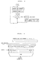
- The rationale of this invention may be extended to apply to the modem receiver filter. The input samples derived from the received signal are fed into a receive (Hilbert) filter delay line at the rate of 21 samples per 4T which corresponds to a sampling frequency of 14400 Hz. The receive filter issues two complex symbols per time T (or 8 per 4T) which are then fed into a T/2-spaced equalizer delay line. The filter impulse response is sampled at a rate corresponding to the lowest common multiple of twice the symbol rate (2/T) and the A/D sampling frequency.

with K1 and K2 being the lowest integer values verifying the above equation.

Assuming the original impulse response was sampled to provide 54 coefficients over T/6 second, then, the number of coefficients for the multirate receive filter for the same length would be

These coefficients are divided into 8 sets of coefficients corresponding to the 8 symbols generated per 4T. The number of coefficients is reduced to N'p = 376 coefficients or 8 sets of 47 coefficients, namely:


A block diagram representation of the receive filter is shown in Figure 3. The incoming samples are fed into a 47 samples long delay line. After 4T, the sample Sn has been shifted by 21 positions and is stored into Sn-21. The different sets of 47 coefficients each, numbered Set(0) to Set(7), are stored in a memory (not shown). They are used in a specific order such that:

- In addition, before each output sample computation, the delay line contents is shifted by a number of samples given by the quotient of the division of the new index by 8.

In other words, assuming the previous set number be i, then i+21 = 8k+n,then, the new set reference number should equal to n and the number of shifts equals to k. - For instance, lets assume the process starts with feeding the Sn input sample into the filter delay line. The output samples are computed and provided as follows:


- Number of shifts = 2. Therefore, no output sample is computed when Sn+1 is fed into the filter delay line. Next sample computation X occurs with Sn+2 arrival.


The process starts rescanning the coefficients sets, i.e. Set(0), Set(5), Set(2), Set(7), Set(4), Set(1), Set(6), Set(4), etc... - In summary, the algorithm may be expressed by:

For twenty one input samples, the filter provides eight output samples using the eight sets of coefficients Set(0) through Set(7) in a fixed order defined by the above equation.
Claims (3)
- A process for performing a digital signal filtering function with a filter impulse response h(t), while operating a rate conversion for providing the filtered output samples at a rate B while the filter is being fed at an input rate A, with A and B relatively prime, said process including:- deriving Np filter coefficients C(i), i=0, 1, ..., Np-1, by sampling said impulse response h(t) at a rate P, with:

wherein "a" and "b" are integer values selected such that P be the lowest multiple value of both A and B;- splitting said Np coefficients into "a" sets, referenced Set(i) with i = 0, 1, ..., a-1, each set including N'p/a coefficients with N'p being substantially equal to Np, each set including the coefficients {C(i), C(i+A), C(i+2.A),.... C(i+N.a)}, N being an integer, and storing said sets of coefficients;- computing "a" output samples while "b" input samples are being fed into the filter, each output sample computation involving using one Set(i), i being repetitively permutated in such a manner that each new set index inew be derived from the previous set index iold from:

- A process according to claim 1 wherein said filter input rate A is higher than the output rate B, whereby each output sample computation involves shifting the input samples k positions into said filter , with k being the quotient of the division of "a" plus the previous coefficient set index, by "b".
- A digital filter having a predefined impulse response h(t) for filtering an input signal sampled at a rate A into a filtered output signal sampled at a rate B, A and B being relatively prime, said filter including shift register means provided with N tap means, a set of N multiplier means having one input connected to one of said taps respectively, adding means connected to said multiplier means, and storage means for storing filter coefficients to be respectively applied to a second input of said multiplier means, said filter being characterized in that it includes:- means for sampling h(t) at a rate substantially equal to the lowest common multiple P of A and B, i.e.
 - means for arranging a number N'p of said coefficients, N'p being substantially equal to Np, into "a" sets of coefficients, Set(i), i = 0, 1, ..., (a-1), with Set(i) including { Ci, C(i+a), C(i+2a), ..., C(i+N.a) }, N being an integer;- means for feeding said input signal samples into said shift register means at said input rate; and,- means for fetching said sets of filter coefficients in a predetermined permutated order defined by
 - means for feeding said multipliers outputs into said adding means;
whereby the output samples are being generated at the output of said adding means at said rate B.
Priority Applications (4)
| Application Number | Priority Date | Filing Date | Title |
|---|---|---|---|
| DE3888830T DE3888830T2 (en) | 1988-08-30 | 1988-08-30 | Measures to improve the method and device of a digital frequency conversion filter. |
| EP88480021A EP0356597B1 (en) | 1988-08-30 | 1988-08-30 | Improvement to digital filter sampling rate conversion method and device |
| JP1154806A JPH0787335B2 (en) | 1988-08-30 | 1989-06-19 | Digital filter and filter method |
| US07/559,533 US5111417A (en) | 1988-08-30 | 1990-07-19 | Digital filter sampling rate conversion method and device |
Applications Claiming Priority (1)
| Application Number | Priority Date | Filing Date | Title |
|---|---|---|---|
| EP88480021A EP0356597B1 (en) | 1988-08-30 | 1988-08-30 | Improvement to digital filter sampling rate conversion method and device |
Publications (2)
| Publication Number | Publication Date |
|---|---|
| EP0356597A1 EP0356597A1 (en) | 1990-03-07 |
| EP0356597B1 true EP0356597B1 (en) | 1994-03-30 |
Family
ID=8200498
Family Applications (1)
| Application Number | Title | Priority Date | Filing Date |
|---|---|---|---|
| EP88480021A Expired - Lifetime EP0356597B1 (en) | 1988-08-30 | 1988-08-30 | Improvement to digital filter sampling rate conversion method and device |
Country Status (4)
| Country | Link |
|---|---|
| US (1) | US5111417A (en) |
| EP (1) | EP0356597B1 (en) |
| JP (1) | JPH0787335B2 (en) |
| DE (1) | DE3888830T2 (en) |
Families Citing this family (27)
| Publication number | Priority date | Publication date | Assignee | Title |
|---|---|---|---|---|
| DE3888830T2 (en) | 1988-08-30 | 1994-11-24 | Ibm | Measures to improve the method and device of a digital frequency conversion filter. |
| US5182559A (en) * | 1989-07-28 | 1993-01-26 | Alpine Electronics, Inc. | Digital-analog converter with plural coefficient transversal filter |
| JPH10294646A (en) * | 1990-02-16 | 1998-11-04 | Sony Corp | Sampling rate conversion device |
| JP3177978B2 (en) * | 1990-07-18 | 2001-06-18 | カシオ計算機株式会社 | Digital filter coefficient setting method |
| US5268750A (en) * | 1992-03-31 | 1993-12-07 | Panasonic Technologies, Inc. | Apparatus for adjusting the timing of sampled data signals in a resampling system |
| GB9301704D0 (en) * | 1993-01-28 | 1993-03-17 | Signal Processors Ltd | New digital modem design techniques |
| US5619202A (en) * | 1994-11-22 | 1997-04-08 | Analog Devices, Inc. | Variable sample rate ADC |
| US5712635A (en) * | 1993-09-13 | 1998-01-27 | Analog Devices Inc | Digital to analog conversion using nonuniform sample rates |
| US5574454A (en) * | 1993-09-13 | 1996-11-12 | Analog Devices, Inc. | Digital phase-locked loop utilizing a high order sigma-delta modulator |
| US5892468A (en) * | 1993-09-13 | 1999-04-06 | Analog Devices, Inc. | Digital-to-digital conversion using nonuniform sample rates |
| US5625358A (en) * | 1993-09-13 | 1997-04-29 | Analog Devices, Inc. | Digital phase-locked loop utilizing a high order sigma-delta modulator |
| US5963160A (en) * | 1993-09-13 | 1999-10-05 | Analog Devices, Inc. | Analog to digital conversion using nonuniform sample rates |
| EP0719477A1 (en) * | 1993-09-13 | 1996-07-03 | Analog Devices, Inc. | Analog to digital conversion using nonuniform sample rates |
| EP0719478B1 (en) * | 1993-09-13 | 1998-07-22 | Analog Devices, Inc. | Digital to analog conversion using nonuniform sample rates |
| EP0695032B1 (en) * | 1994-07-25 | 2001-11-07 | Matsushita Electric Industrial Co., Ltd. | Digital-to-digital sample rate converter |
| US5613084A (en) * | 1994-10-04 | 1997-03-18 | Panasonic Technologies, Inc. | Interpolation filter selection circuit for sample rate conversion using phase quantization |
| US5512897A (en) * | 1995-03-15 | 1996-04-30 | Analog Devices, Inc. | Variable sample rate DAC |
| US5732002A (en) * | 1995-05-23 | 1998-03-24 | Analog Devices, Inc. | Multi-rate IIR decimation and interpolation filters |
| US5638010A (en) * | 1995-06-07 | 1997-06-10 | Analog Devices, Inc. | Digitally controlled oscillator for a phase-locked loop providing a residue signal for use in continuously variable interpolation and decimation filters |
| KR0178742B1 (en) * | 1995-10-21 | 1999-05-01 | 김광호 | The memory control signal and address generating apparatus for data companding |
| US5814750A (en) * | 1995-11-09 | 1998-09-29 | Chromatic Research, Inc. | Method for varying the pitch of a musical tone produced through playback of a stored waveform |
| US6313765B1 (en) | 1997-10-10 | 2001-11-06 | L-3 Communications Corporation | Method for sample rate conversion of digital data |
| US6351730B2 (en) * | 1998-03-30 | 2002-02-26 | Lucent Technologies Inc. | Low-complexity, low-delay, scalable and embedded speech and audio coding with adaptive frame loss concealment |
| US6341048B1 (en) | 1999-01-25 | 2002-01-22 | Seagate Technology Llc | Method and apparatus for servo data synchronization in a disc drive |
| US6785080B1 (en) * | 2000-10-10 | 2004-08-31 | Maxtor Corporation | Method and apparatus for providing a variable rate oversampling digital filter for resonance compensation in disk drive servo control systems |
| US6766339B2 (en) * | 2001-01-11 | 2004-07-20 | Asml Holding N.V. | Method and system for efficient and accurate filtering and interpolation |
| JP5274014B2 (en) * | 2004-10-13 | 2013-08-28 | メディアテック インコーポレーテッド | Communication system filter |
Family Cites Families (14)
| Publication number | Priority date | Publication date | Assignee | Title |
|---|---|---|---|---|
| US4020332A (en) * | 1975-09-24 | 1977-04-26 | Bell Telephone Laboratories, Incorporated | Interpolation-decimation circuit for increasing or decreasing digital sampling frequency |
| JPS5428520A (en) * | 1977-08-08 | 1979-03-03 | Hitachi Ltd | Method and apparatus for sampling frequency conversion |
| ATE14358T1 (en) * | 1980-11-26 | 1985-08-15 | Studer Willi Ag | METHOD AND CIRCUIT ARRANGEMENT FOR CONVERTING THE SAMPLING FREQUENCY OF A SAMPLING SERIES, BYPASSING CONVERSION TO A CONTINUOUS SIGNAL. |
| JPS58219841A (en) * | 1982-06-15 | 1983-12-21 | Kokusai Denshin Denwa Co Ltd <Kdd> | High speed converting circuit of sampled frequency |
| NL8202687A (en) * | 1982-07-05 | 1984-02-01 | Philips Nv | DECIMATING FILTER DEVICE. |
| JPS59105712A (en) * | 1982-12-09 | 1984-06-19 | Fujitsu Ltd | Digital filter |
| ATE37972T1 (en) * | 1983-07-14 | 1988-10-15 | Ant Nachrichtentech | METHOD OF MATCHING TWO SYSTEMS WITH DIFFERENT SAMPLING RATE. |
| NL8400073A (en) * | 1984-01-10 | 1985-08-01 | Philips Nv | INTERPOLATING FILTERING DEVICE WITH NON-RATIONAL RATIO BETWEEN THE INPUT AND OUTPUT SAMPLING FREQUENCIES. |
| JPS61100015A (en) * | 1984-10-22 | 1986-05-19 | Nippon Precision Saakitsutsu Kk | Digital filter for sampling frequency conversion |
| GB2180114A (en) * | 1985-04-13 | 1987-03-18 | Plessey Co Plc | Digital filters |
| JPS6367913A (en) * | 1986-09-10 | 1988-03-26 | Fujitsu Ltd | Method for converting time sequential numerical data |
| JPH0744425B2 (en) * | 1986-12-29 | 1995-05-15 | 日本電気ホームエレクトロニクス株式会社 | Digital filtering circuit |
| JPH0793548B2 (en) * | 1987-08-31 | 1995-10-09 | 三洋電機株式会社 | Sampling frequency conversion circuit |
| DE3888830T2 (en) | 1988-08-30 | 1994-11-24 | Ibm | Measures to improve the method and device of a digital frequency conversion filter. |
-
1988
- 1988-08-30 DE DE3888830T patent/DE3888830T2/en not_active Expired - Fee Related
- 1988-08-30 EP EP88480021A patent/EP0356597B1/en not_active Expired - Lifetime
-
1989
- 1989-06-19 JP JP1154806A patent/JPH0787335B2/en not_active Expired - Lifetime
-
1990
- 1990-07-19 US US07/559,533 patent/US5111417A/en not_active Expired - Lifetime
Also Published As
| Publication number | Publication date |
|---|---|
| JPH0787335B2 (en) | 1995-09-20 |
| DE3888830T2 (en) | 1994-11-24 |
| DE3888830D1 (en) | 1994-05-05 |
| US5111417A (en) | 1992-05-05 |
| EP0356597A1 (en) | 1990-03-07 |
| JPH0282806A (en) | 1990-03-23 |
Similar Documents
| Publication | Publication Date | Title |
|---|---|---|
| EP0356597B1 (en) | Improvement to digital filter sampling rate conversion method and device | |
| US6678709B1 (en) | Digital filter with efficient quantization circuitry | |
| US7920078B2 (en) | Systems and methods for variable rate conversion | |
| JP2724188B2 (en) | Digital interpolation device | |
| US6512468B1 (en) | System and method for increasing sample rate converter filter coefficient derivation speed | |
| KR100373525B1 (en) | Methods and apparatus for variable-rate down-sampling filters for discrete-time sampled systems using a fixed sampling rate | |
| EP0227172B1 (en) | Phase-locked loop coefficient generator for a filter arrangement having a non-rational ratio between input and output sampling frequencies | |
| EP0695032B1 (en) | Digital-to-digital sample rate converter | |
| US4270026A (en) | Interpolator apparatus for increasing the word rate of a digital signal of the type employed in digital telephone systems | |
| US20040120361A1 (en) | Asynchronous sample rate converter and method | |
| EP0977360A2 (en) | Improved FIR filter structure with time-varying coefficients and filtering method for digital data scaling | |
| US7196648B1 (en) | Non-integer decimation using cascaded intergrator-comb filter | |
| GB2363924A (en) | Processor for FIR filtering | |
| JP3858160B2 (en) | Timing interpolator in a digital demodulator. | |
| US7324025B1 (en) | Non-integer interpolation using cascaded integrator-comb filter | |
| GB2064902A (en) | Telephone line circuit | |
| US7248189B2 (en) | Programmable sample rate conversion engine for wideband systems | |
| US6522275B2 (en) | Method and apparatus for sample rate conversion for use in an analog to digital converter | |
| US6188723B1 (en) | Finite impulse response filter for wave-shaping digital quadrature amplitude modulation symbols | |
| US6000834A (en) | Audio sampling rate conversion filter | |
| US20040052300A1 (en) | Digital sampling rate conversion using a poly-phase filter and a polynomial interpolator | |
| US6438567B2 (en) | Method for selective filtering | |
| EP0657999B1 (en) | Sampling frequency conversion | |
| US6772022B1 (en) | Methods and apparatus for providing sample rate conversion between CD and DAT | |
| US9030337B2 (en) | Multi-branch down converting fractional rate change filter |
Legal Events
| Date | Code | Title | Description |
|---|---|---|---|
| PUAI | Public reference made under article 153(3) epc to a published international application that has entered the european phase |
Free format text: ORIGINAL CODE: 0009012 |
|
| AK | Designated contracting states |
Kind code of ref document: A1 Designated state(s): DE FR GB |
|
| 17P | Request for examination filed |
Effective date: 19900621 |
|
| 17Q | First examination report despatched |
Effective date: 19921120 |
|
| GRAA | (expected) grant |
Free format text: ORIGINAL CODE: 0009210 |
|
| AK | Designated contracting states |
Kind code of ref document: B1 Designated state(s): DE FR GB |
|
| REF | Corresponds to: |
Ref document number: 3888830 Country of ref document: DE Date of ref document: 19940505 |
|
| ET | Fr: translation filed | ||
| PLBE | No opposition filed within time limit |
Free format text: ORIGINAL CODE: 0009261 |
|
| STAA | Information on the status of an ep patent application or granted ep patent |
Free format text: STATUS: NO OPPOSITION FILED WITHIN TIME LIMIT |
|
| 26N | No opposition filed | ||
| PGFP | Annual fee paid to national office [announced via postgrant information from national office to epo] |
Ref country code: DE Payment date: 19990816 Year of fee payment: 12 |
|
| PGFP | Annual fee paid to national office [announced via postgrant information from national office to epo] |
Ref country code: FR Payment date: 20000801 Year of fee payment: 13 |
|
| PGFP | Annual fee paid to national office [announced via postgrant information from national office to epo] |
Ref country code: GB Payment date: 20000803 Year of fee payment: 13 |
|
| PG25 | Lapsed in a contracting state [announced via postgrant information from national office to epo] |
Ref country code: DE Free format text: LAPSE BECAUSE OF NON-PAYMENT OF DUE FEES Effective date: 20010501 |
|
| PG25 | Lapsed in a contracting state [announced via postgrant information from national office to epo] |
Ref country code: GB Free format text: LAPSE BECAUSE OF NON-PAYMENT OF DUE FEES Effective date: 20010830 |
|
| PG25 | Lapsed in a contracting state [announced via postgrant information from national office to epo] |
Ref country code: FR Free format text: LAPSE BECAUSE OF NON-PAYMENT OF DUE FEES Effective date: 20020430 |
|
| REG | Reference to a national code |
Ref country code: FR Ref legal event code: ST |