EP0348539A1 - Programmable CMOS logic array - Google Patents
Programmable CMOS logic array Download PDFInfo
- Publication number
- EP0348539A1 EP0348539A1 EP88110267A EP88110267A EP0348539A1 EP 0348539 A1 EP0348539 A1 EP 0348539A1 EP 88110267 A EP88110267 A EP 88110267A EP 88110267 A EP88110267 A EP 88110267A EP 0348539 A1 EP0348539 A1 EP 0348539A1
- Authority
- EP
- European Patent Office
- Prior art keywords
- line
- row
- area
- dummy
- column
- Prior art date
- Legal status (The legal status is an assumption and is not a legal conclusion. Google has not performed a legal analysis and makes no representation as to the accuracy of the status listed.)
- Withdrawn
Links
Images
Classifications
-
- H—ELECTRICITY
- H03—ELECTRONIC CIRCUITRY
- H03K—PULSE TECHNIQUE
- H03K5/00—Manipulating of pulses not covered by one of the other main groups of this subclass
- H03K5/13—Arrangements having a single output and transforming input signals into pulses delivered at desired time intervals
- H03K5/14—Arrangements having a single output and transforming input signals into pulses delivered at desired time intervals by the use of delay lines
-
- G—PHYSICS
- G11—INFORMATION STORAGE
- G11C—STATIC STORES
- G11C7/00—Arrangements for writing information into, or reading information out from, a digital store
- G11C7/22—Read-write [R-W] timing or clocking circuits; Read-write [R-W] control signal generators or management
-
- H—ELECTRICITY
- H03—ELECTRONIC CIRCUITRY
- H03K—PULSE TECHNIQUE
- H03K19/00—Logic circuits, i.e. having at least two inputs acting on one output; Inverting circuits
- H03K19/02—Logic circuits, i.e. having at least two inputs acting on one output; Inverting circuits using specified components
- H03K19/173—Logic circuits, i.e. having at least two inputs acting on one output; Inverting circuits using specified components using elementary logic circuits as components
- H03K19/177—Logic circuits, i.e. having at least two inputs acting on one output; Inverting circuits using specified components using elementary logic circuits as components arranged in matrix form
- H03K19/17704—Logic circuits, i.e. having at least two inputs acting on one output; Inverting circuits using specified components using elementary logic circuits as components arranged in matrix form the logic functions being realised by the interconnection of rows and columns
- H03K19/17708—Logic circuits, i.e. having at least two inputs acting on one output; Inverting circuits using specified components using elementary logic circuits as components arranged in matrix form the logic functions being realised by the interconnection of rows and columns using an AND matrix followed by an OR matrix, i.e. programmable logic arrays
- H03K19/17716—Logic circuits, i.e. having at least two inputs acting on one output; Inverting circuits using specified components using elementary logic circuits as components arranged in matrix form the logic functions being realised by the interconnection of rows and columns using an AND matrix followed by an OR matrix, i.e. programmable logic arrays with synchronous operation, i.e. using clock signals, e.g. of I/O or coupling register
- H03K19/1772—Logic circuits, i.e. having at least two inputs acting on one output; Inverting circuits using specified components using elementary logic circuits as components arranged in matrix form the logic functions being realised by the interconnection of rows and columns using an AND matrix followed by an OR matrix, i.e. programmable logic arrays with synchronous operation, i.e. using clock signals, e.g. of I/O or coupling register with synchronous operation of at least one of the logical matrixes
Definitions
- the invention relates to the improvement of non-overlapping two-phase clocked, technically complementary insulating layer field-effect transistors, programmable Lokig fields, i.e. abbreviated CMOS-PLAs, as described in the book by N.H.E. Weste et al "Principles of CMOS-VLSI Design", Reading, Massachusetts, 1985, pages 368-373, in particular chapter 8.7.4 (pages 372/373).
- CMOS-PLAs programmable Lokig fields
- CMOS-PLAs have an AND area, an OR area and an AND / OR area connecting these two to each other, their respective transistors in m rows and n columns of the AND area and in p columns of the OR area between each a first and a second row line or between a first and a second column line.
- the internal clocking serves a dummy line in the AND and AND / OR area, which also has two line lines, and a Schmitt trigger, the input of which is connected to the first line line of the dummy line.
- a precharge P transistor and an Evaluate N transistor are provided, the gates of which in the rows and in the dummy row are inverted by the first two-phase transistor. Clock or in the columns are driven by the output signal of the Schmitt trigger.
- the respective controlled current path of the precharge P transistors between an operating voltage and the first row or column line and that of the Evaluate N transistor between the circuit zero and the second row or column line.
- two N-transistors are provided in the dummy row in the AND area, the controlled current paths of which lie between the first and the second row line and of which the gate of the one with the first column line and the gate of the other with the second column line connected is.
- CMOS-PLA complementary metal-oxide-semiconductor
- one of the phases of the non-overlapping two-phase clock is used to store the input signals in the AND region, while an internal clock signal by means of the dummy line and the one mentioned is used for clocking the OR region Schmitt triggers is generated.
- This must have a greater delay than the evaluation time in each line of the AND and OR areas. This is determined by the respective load capacitance and the area of the row and column transistors.
- the load capacitance essentially consists of the capacitance of the source or drain zones of these transistors.
- the number of line transistors is greatest when there is a line transistor between each input of the CMOS-PLA, ie either the non-inverted or inverted input signal, and the corresponding minterm.
- the greatest evaluation time arises if, in such a term, only one line transistor has to reload the line capacitance due to the input signals.
- the dummy line and the Schmitt trigger are provided in the CMOS-PLA described above. Due to the transistors in the dummy line, the load capacity of this line is twice as large as that of the worst case explained within the AND range.
- CMOS PLAs manufactured as integrated circuits manufacturing process-dependent fluctuations in the delay.
- the invention now seeks to remedy this, the task of which is to modify and improve the above-described CMOS PLA in such a way that the production-related delay fluctuations are substantially reduced.
- the Schmitt trigger is also to be replaced by a subcircuit having fewer transistors.
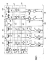
- the columns us1, us2, usn are shown in the drawings from the n columns of the AND region, while the columns os1, osp are shown from the p columns of the OR region.
- the lines z1, zm and additionally the dummy line zd can be seen in FIG. 1.
- the AND / OR area uob lies between the AND area ub and the OR area ob.
- Each row has the two row lines lz1, lz2, the latter only being present in the AND area, but the former leading into the OR area, usually with two inverters connected in series in terms of signal flow in the AND / OR area, via which the signal of the row line lz1 is carried to refresh the level.
- the columns also each have the two column lines ls1, ls2.
- Those of the AND area carry the non-inverted and the inverted input signal, which leads from the respective input e1, e2, en via the respective input transmission gate tge, which is controlled by the first clock signal f1, and via the two inverters i1, i2 is.
- the first column line ls1 lies at the output of the inverter i1 and the second column line ls2 lies at that of the second inverter i2.
- the first column line ls1 lies via the output transmission gate tga, which is controlled by the second clock signal f2, and the third inverter i3 at the respective output a1, ap.
- the dummy line zd also has the in the AND area two row lines ld1, ld2, of which the first row line ld1 is connected to one input of the NOR gate ng, while the other input of which is connected to the reset line lr.
- the pre-charge P transistor tpz, tps is provided, the controlled current path of which connects the respective first row line lz1, ld1 and the respective column line ls1 to the operating voltage source u. Furthermore, in each row, the dummy row and each column of the OR area, there is provided whether the evaluate-N transistor tez, tes, whose controlled current path connects the respective second row or column line lz2, ld2, ls2 to the circuit zero. In each line and in the dummy line, the gates of the two transistors tpz, tez are connected to one another and driven by the inverted first clock signal f1q. In each column of the OR area ob, the gates of the two transistors tps, tes are also connected to one another, but are driven by the output of the OR gate ng.
- the controlled current path of the column transistor ts whose gate is connected to the respective first row line lz1, likewise lies between the two column lines ls1, ls2 of each column in accordance with the intended programming.
- 1 of the possible column transistors ts are the OR cells formed in the row z1 and the columns os1, osp and the column transistors in the OR cell formed by the row zm and the column os1.
- the two capacitors c are provided per column, one of which lies between the first row line ld1 and the circuit zero point and the other of which lies between the second row line ld2 and the circuit zero point.
- 2n capacitors c are therefore present.
- this is not mandatory, but it can also be fewer, although at least twice as many capacitors must be present as are present in the line of the AND region (ub) which contains the most line transistors tz of all these lines.
- the capacitors c are formed by zones (d in FIG. 2) which are doped in the opposite direction to the substrate and which in each case have the same area and if possible the same Edge length as the zone connected to the first or second row line lz1, lz2, that is to say either source or drain, of the respective row transistor tz.
- the capacitors c are thus connected to the circuit zero via the substrate.
- the N-transistor t which lies between its row lines ld1, ld2 with its controlled current path but is arranged outside the AND region and whose gate is connected to the operating voltage source u.
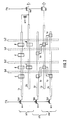
- FIG. 2 In the schematic combined layout circuit diagram shown in FIG. 2 of an exemplary embodiment of the second solution variant of the invention, it is first shown that in each case two adjacent lines including the dummy line according to FIG. 1, the second line lines lz2, ld2 are combined to form the pair line lp can, so that in each of these line pairs instead of the two Evaluate-N transistors the corresponding transistor tez 'is to be provided.
- the line line still remaining for each line and the dummy line is provided with the reference symbol lz throughout in FIG. 2.
- the brackets on the left edge of FIG. 2 indicate which lines of FIG. 1 are represented by the arrangement of FIG. 2.
- FIG. 2 schematically shows the layout in the AND area.
- the horizontal stripes represent interconnects, e.g. made of aluminum, while the vertical, dotted strips also represent interconnects, but preferably made of polycrystalline silicon, and the column lines are.
- corresponding line transistors tz are shown schematically with their layout, namely a transistor between the lower line line lz and the pair line lp or between this and the upper line line lz .
- the drain or source connection of the respective row transistor the channel zone of which is at the intersection of the horizontal transistor part with the respective column line.
- the strongly bordered areas between the mentioned connection area and the channel area are the respective drain or source zones.
- a row transistor tz with its gate is connected to row line ls1, while in the right part of FIG. 2 the lower row transistor tz is connected with its gate to column line ls2.
- zones d are to be provided for each AND cell in the dummy row zd, the maximum number of which is 3n, but there are at least three times as many as in that row of the AND Range, which contains the most line transistors of all these lines.
- Two thirds of zones d are with Row line lz of the dummy row zd and a third contacted with their pair line lp. These zones also have the same area and the same edge length as possible as the zones of the assigned line transistors tz.
- FIG. 2 also shows the N transistor t, which is arranged in the dummy line zd between the line line lz and the pair line lp with its controlled current path and whose gate is connected to the operating voltage source u.
Landscapes
- Physics & Mathematics (AREA)
- Mathematical Physics (AREA)
- Nonlinear Science (AREA)
- Engineering & Computer Science (AREA)
- Computer Hardware Design (AREA)
- Computing Systems (AREA)
- General Engineering & Computer Science (AREA)
- Logic Circuits (AREA)
- Design And Manufacture Of Integrated Circuits (AREA)
Abstract
Description
Die Erfindung betrifft die schaltungstechnischhalbleitertechnologische Verbesserung von nichtüberlappend zweiphasen-getakteten, in der Technik komplementärer Isolierschicht-Feldeffekttransistoren realisierten programmierbaren Lokig-Feldern, also abgekürzt CMOS-PLAs, wie sie in dem Buch von N.H.E. Weste et al "Principles of CMOS-VLSI Design", Reading, Massachusetts, 1985, Seiten 368-373, insbesondere Kapitel 8.7.4 (Seiten 372/373) beschrieben sind.The invention relates to the improvement of non-overlapping two-phase clocked, technically complementary insulating layer field-effect transistors, programmable Lokig fields, i.e. abbreviated CMOS-PLAs, as described in the book by N.H.E. Weste et al "Principles of CMOS-VLSI Design", Reading, Massachusetts, 1985, pages 368-373, in particular chapter 8.7.4 (pages 372/373).
Derartige CMOS-PLAs haben einen UND-Bereich, einen ODER-Bereich und einen diese beiden untereinander verbindenden UND/ODER-Bereich, deren jeweilige Transistoren in m Zeilen sowie n Spalten des UND-Bereichs und in in p Spalten des ODER-Bereichs zwischen jeweils einer ersten und einer zweiten Zeilenleitung bzw. zwischen jeweils einer ersten und einer zweiten Spaltenleitung angeordnet sind. Der internen Taktung dient eine Dummy-Zeile im UND- sowie UND/ODER-Bereich, die ebenfalls zwei Zeilenleitungen hat, sowie ein Schmitt-Trigger, dessen Eingang mit der ersten Zeilenleitung der Dummy-Zeile verbunden ist. Ferner ist in jeder Zeile, in der Dummy-Zeile und in jeder Spalte des ODER-Bereichs ein Precharge-P-Transistor und ein Evaluate-N-Tansistor vorgesehen, deren Gates in den Zeilen und in der Dummy-Zeile vom invertierten ersten Zweiphasen-Takt bzw. in den Spalten vom Ausgangssignal des Schmitt-Triggers angesteuert sind. Dabei liegt der jeweilige gesteuerte Strompfad der Precharge-P-Transistoren zwischen einer Betriebsspannung und der ersten Zeilen- bzw. Spaltenleitung und der des Evaluate-N-Transistors zwischen dem Schaltungsnullpunkt und der zweiten Zeilen- bzw. Spaltenleitung. Schließlich sind im UND-Bereich in der Dummy-Zeile pro Spalte zwei N-Transistoren vorgesehen, deren gesteuerte Strompfade zwischen der ersten und der zweiten Zeilenleitung liegen und von denen das Gate des einen mit der ersten Spaltenleitung und das Gate des anderen mit der zweiten Spaltenleitung verbunden ist. Die Programmierung erfolgt durch Spalten- und Zeilentransistoren, wobei die letzteren im UND-Bereich mit ihrem gesteuerten Strompfad zwischen den beiden Zeilenleitungen einer Zeile angeordnet sind und deren Gate entweder vom nichtinvertierten oder invertierten Eingangssignal angesteuert ist, während die Spaltentransistoren im ODER-Bereich mit ihrem gesteuerten Strompfad zwischen der ersten und der zweiten Spaltenleitung liegen, von denen die erste zum Ausgang führt. Die Anzahl der Zeilen- und Spaltentransistoren und ihre jeweilige Lage im UND- und ODER-Bereich wird durch die beabsichtigte Programmierung bestimmt. Weitere Einzelheiten werden unten in Zusammenhang mit der Erläuterung der Fig. 1 angegeben.Such CMOS-PLAs have an AND area, an OR area and an AND / OR area connecting these two to each other, their respective transistors in m rows and n columns of the AND area and in p columns of the OR area between each a first and a second row line or between a first and a second column line. The internal clocking serves a dummy line in the AND and AND / OR area, which also has two line lines, and a Schmitt trigger, the input of which is connected to the first line line of the dummy line. Furthermore, in each row, in the dummy row and in each column of the OR area, a precharge P transistor and an Evaluate N transistor are provided, the gates of which in the rows and in the dummy row are inverted by the first two-phase transistor. Clock or in the columns are driven by the output signal of the Schmitt trigger. Here lies the respective controlled current path of the precharge P transistors between an operating voltage and the first row or column line and that of the Evaluate N transistor between the circuit zero and the second row or column line. Finally, two N-transistors are provided in the dummy row in the AND area, the controlled current paths of which lie between the first and the second row line and of which the gate of the one with the first column line and the gate of the other with the second column line connected is. Programming is carried out by column and row transistors, the latter being arranged in the AND area with its controlled current path between the two row lines of a row and the gate of which is driven either by the non-inverted or inverted input signal, while the column transistors in the OR area are controlled by their Current path between the first and the second column line, of which the first leads to the output. The number of row and column transistors and their respective position in the AND and OR area is determined by the intended programming. Further details are given below in connection with the explanation of FIG. 1.
Bei der vorbeschriebenen CMOS-PLA wird zum Abspeichern der Eingangssignale im UND-Bereich eine der Phasen des nichtüberlappenden Zweiphasen-Takts verwendet, während für die Taktung des ODER-Bereichs ein internes Taktsignal mittels der Dummy-Zeile und des erwähnten Schmitt-Triggers erzeugt wird. Dieses muß eine größere Verzögerung aufweisen, als die Auswertzeit in jeder Zeile von UND- und ODER-Bereich beträgt. Diese wird durch die jeweilige Lastkapazität und die Fläche der Zeilen- und Spaltentransistoren bestimmt. Die Lastkapazität setzt sich im wesentlichen aus der Kapazität der Source- bzw. Drainzonen dieser Transistoren zusammen.In the CMOS-PLA described above, one of the phases of the non-overlapping two-phase clock is used to store the input signals in the AND region, while an internal clock signal by means of the dummy line and the one mentioned is used for clocking the OR region Schmitt triggers is generated. This must have a greater delay than the evaluation time in each line of the AND and OR areas. This is determined by the respective load capacitance and the area of the row and column transistors. The load capacitance essentially consists of the capacitance of the source or drain zones of these transistors.
Die Anzahl der Zeilentransistoren ist am größten, wenn zwischen jedem Eingang der CMOS-PLA, also entweder dem nichtinvertierten oder invertierten Eingangssignal, und dem entsprechenden Minterm je ein Zeilentransistor sitzt. Die größte Auswertzeit ergibt sich, wenn in einem solchen Minterm aufgrund der Eingangssignale nur ein Zeilentransistor die Leitungskapazität umladen muß. Um diesen Worst-Case bei der Erzeugung des internen Taktsignals zu berücksichtigen, sind bei der vorbeschriebenen CMOS-PLA die Dummy-Zeile und der Schmitt-Trigger vorgesehen. Durch die in der Dummy-Zeile liegenden Transistoren ist die Lastkapazität dieser Zeile doppelt so groß wie die des erläuterten Worst-Cases innerhalb des UND-Bereichs.The number of line transistors is greatest when there is a line transistor between each input of the CMOS-PLA, ie either the non-inverted or inverted input signal, and the corresponding minterm. The greatest evaluation time arises if, in such a term, only one line transistor has to reload the line capacitance due to the input signals. In order to take this worst case into account when generating the internal clock signal, the dummy line and the Schmitt trigger are provided in the CMOS-PLA described above. Due to the transistors in the dummy line, the load capacity of this line is twice as large as that of the worst case explained within the AND range.
Bei der vorbeschriebenen Anordnung ist nicht nur die Hälfte der Transistoren der Dummy-Zeile dauernd stromführend, sondern durch den Schmitt-Trigger und dessen zusätzliche Verzögerung des internen Taktsignals wird auch noch nicht vollständig erreicht, daß Fehlfunktionen ausgeschlossen sind. Hinzu kommt, daß die als integrierte Schaltungen hergestellten CMOS-PLAs herstellungsprozeßabhängige Schwankungen der Verzögerung aufweisen.In the arrangement described above, not only is half of the transistors of the dummy line continuously live, but the Schmitt trigger and its additional delay of the internal clock signal also do not completely ensure that malfunctions are excluded. In addition, the CMOS PLAs manufactured as integrated circuits manufacturing process-dependent fluctuations in the delay.
Hier will nun die Erfindung Abhilfe schaffen, deren Aufgabe es ist, die vorbeschriebene CMOS-PLA so abzuwandeln und zu verbessern, daß die herstellungsbedingten Verzögerungsschwankungen wesentlich reduziert sind. Auch soll der Schmitt-Trigger durch eine weniger Transistoren aufweisende Teilschaltung ersetzt werden.The invention now seeks to remedy this, the task of which is to modify and improve the above-described CMOS PLA in such a way that the production-related delay fluctuations are substantially reduced. The Schmitt trigger is also to be replaced by a subcircuit having fewer transistors.
Dies gelingt bei der Erfindung im wesentlichen dadurch, daß anstatt der Transistoren der Dummy-Zeile lediglich die in den Ansprüchen im einzelnen definierten Kondensatoren sowie der dort angegebene N-Transistor vorgesehen sind und daß der Schmitt-Trigger durch das NOR-Gatter ersetzt ist.This is achieved in the invention essentially in that instead of the transistors of the dummy line, only the capacitors defined in the claims and the N-transistor specified there are provided and that the Schmitt trigger is replaced by the NOR gate.
Die Erfindung wird nun anhand der Figuren der Zeichnungen näher erläutert.
- Fig. 1 zeigt in schematischer Schaltbild-Darstellung ein Ausführungsbeispiel der ersten Lösungsvariante der Erfindung mit zwei Zeilenleitungen pro Zeile, und
- Fig. 2 zeigt in schematischer Layout- und Schaltbilddarstellung ein Ausführungsbeispiel der zweiten Lösungsvariante der Erfindung.
- Fig. 1 shows a schematic circuit diagram representation of an embodiment of the first solution of the invention with two row lines per row, and
- 2 shows a schematic layout and circuit diagram representation of an embodiment of the second variant of the invention.
Bei dem in Fig. 1 in schematischer Schaltbilddarstellung gezeigten Ausführungsbeispiel der ersten Variante der Erfindung sind von den n Spalten des UND-Bereichs ub die Spalten us1, us2, usn zeichnerisch dargestellt, während von den p Spalten des ODER-Bereichs ob die Spalten os1, osp gezeigt sind. Von den m Zeilen sind die Zeilen z1, zm und zusätzlich die Dummy-Zeile zd in Fig. 1 zu sehen. Zwischen dem UND-Bereich ub und dem ODER-Bereich ob liegt der UND/ODER-Bereich uob. Jede Zeile hat die beiden Zeilenleitungen lz1, lz2, wobei die letztere lediglich im UND-Bereich vorhanden ist, die erstere jedoch bis in den ODER-Bereich hineinführt, wobei üblicherweise im UND/ODER-Bereich zwei signalflußmäßig in Serie geschaltete Inverter liegen, über die zur Pegelauffrischung das Signal der Zeilenleitung lz1 geführt ist.In the exemplary embodiment of the first variant of FIG. 1 shown in a schematic circuit diagram Invention, the columns us1, us2, usn are shown in the drawings from the n columns of the AND region, while the columns os1, osp are shown from the p columns of the OR region. Of the m lines, the lines z1, zm and additionally the dummy line zd can be seen in FIG. 1. The AND / OR area uob lies between the AND area ub and the OR area ob. Each row has the two row lines lz1, lz2, the latter only being present in the AND area, but the former leading into the OR area, usually with two inverters connected in series in terms of signal flow in the AND / OR area, via which the signal of the row line lz1 is carried to refresh the level.
Auch die Spalten haben jeweils die beiden Spaltenleitungen ls1, ls2. Die des UND-Bereichs führen das nichinvertierte und das invertierte Eingangssignal, das vom jeweiligen Eingang e1, e2, en über das jeweilige Eingangs-Transmission-Gate tge, das vom ersten Taktsignal f1 leitend gesteuert ist, und über die beiden Inverter i1, i2 geführt ist. Am Ausgang des Inverters i1 liegt die erste Spaltenleitung ls1 und an dem des zweiten Inverters i2 die zweite Spaltenleitung ls2.The columns also each have the two column lines ls1, ls2. Those of the AND area carry the non-inverted and the inverted input signal, which leads from the respective input e1, e2, en via the respective input transmission gate tge, which is controlled by the first clock signal f1, and via the two inverters i1, i2 is. The first column line ls1 lies at the output of the inverter i1 and the second column line ls2 lies at that of the second inverter i2.
Im ODER-Bereich liegt die erste Spaltenleitung ls1 über das Ausgangs-Transmission-Gate tga, das vom zweiten Taktsignal f2 leitend gesteuert ist, und den dritten Inverter i3 am jeweiligen Ausgang a1, ap.In the OR area, the first column line ls1 lies via the output transmission gate tga, which is controlled by the second clock signal f2, and the third inverter i3 at the respective output a1, ap.
Die Dummy-Zeile zd hat im UND-Bereich ebenfalls die beiden Zeilenleitungen ld1, ld2, von denen die erste Zeilenleitung ld1 mit dem einen Eingang des NOR-Gatters ng verbunden ist, während dessen anderer Eingang an der Reset-Leitung lr angeschlossen ist.The dummy line zd also has the in the AND area two row lines ld1, ld2, of which the first row line ld1 is connected to one input of the NOR gate ng, while the other input of which is connected to the reset line lr.
In jeder Zeile, in der Dummy-Zeile und in jeder Spalte ist der Precharge-P-Transistor tpz, tps vorgesehen, dessen gesteuerter Strompfad die jeweilige erste Zeilenleitung lz1, ld1 und die jeweilige Spaltenleitung ls1 mit der Betriebsspannungquelle u verbindet. Ferner ist in jeder Zeile, der Dummy-Zeile und jeder Spalte des ODER-Bereichs ob der Evaluate-N-Transistor tez, tes vorgesehen, dessen gesteuerter Strompfad die jeweilige zweite Zeilen- bzw. Spaltenleitung lz2, ld2, ls2 mit dem Schaltungsnullpunkt verbindet. In jeder Zeile und in der Dummy-Zeile sind die Gates der beiden Transistoren tpz, tez miteinander verbunden und vom invertierten ersten Taktsignal f1q angesteuert. In jeder Spalte des ODER-Bereichs ob sind die Gates der beiden Transistoren tps, tes ebenfalls miteinander verbunden, jedoch vom Ausgang des ODER-Gatters ng angesteuert.In each row, in the dummy row and in each column, the pre-charge P transistor tpz, tps is provided, the controlled current path of which connects the respective first row line lz1, ld1 and the respective column line ls1 to the operating voltage source u. Furthermore, in each row, the dummy row and each column of the OR area, there is provided whether the evaluate-N transistor tez, tes, whose controlled current path connects the respective second row or column line lz2, ld2, ls2 to the circuit zero. In each line and in the dummy line, the gates of the two transistors tpz, tez are connected to one another and driven by the inverted first clock signal f1q. In each column of the OR area ob, the gates of the two transistors tps, tes are also connected to one another, but are driven by the output of the OR gate ng.
Im UND-Bereich ub liegt entsprechend der beabsichtigten Programmierung zwischen den beiden Zeilenleitungen lz1, lz2 einer Zeile der gesteuerte Strompfad des Zeilentransistors tz, dessen Gate entweder mit der ersten oder der zweiten Spaltenleitung ls1, ls2 verbunden ist, so daß diese Transistoren entweder vom nichtinvertierten oder vom invertierten Eingangssignal leitend gesteuert werden. In Fig. 1 sind von den möglichen Zeilentransistoren tz diejenigen in den von der Spalte us1 und den Zeilen z1, zm gebildeten UND-Zellen vorhandenen gezeigt.In the AND region ub, according to the intended programming, between the two row lines lz1, lz2 of a row is the controlled current path of the row transistor tz, the gate of which is connected to either the first or the second column line ls1, ls2, so that these transistors either from the non-inverted or controlled by the inverted input signal. In Fig. 1 of the possible line transistors tz are those in the of the column us1 and the rows z1, shown existing AND cells formed.
Im ODER-Bereich ob liegt ebenfalls entsprechend der beabsichtigten Programmierung zwischen den beiden Spaltenleitungen ls1, ls2 jeder Spalte der gesteuerte Strompfad des Spaltentransistors ts, dessen Gate mit der jeweiligen ersten Zeilenleitung lz1 verbunden ist. In Fig. 1 sind von den möglichen Spaltentransistoren ts die in den von der Zeile z1 und den Spalten os1, osp gebildeten ODER-Zellen und die in der von der Zeile zm und der Spalte os1 gebildeten ODER-Zelle liegenden Spaltentransistoren eingezeichnet.In the OR region ob, the controlled current path of the column transistor ts, whose gate is connected to the respective first row line lz1, likewise lies between the two column lines ls1, ls2 of each column in accordance with the intended programming. 1 of the possible column transistors ts are the OR cells formed in the row z1 and the columns os1, osp and the column transistors in the OR cell formed by the row zm and the column os1.
In der Dummy-Zeile zd des UND-Bereichs ub zd sind pro Spalte die beiden Kondensatoren c vorgesehen, deren einer zwischen der ersten Zeilenleitung ld1 und dem Schaltungsnullpunkt und deren anderer zwischen der zweiten Zeilenleitung ld2 und dem Schaltungsnullpunkt liegt. Im Ausführungsbeispiel der Fig. 1 sind also 2n Kondensatoren c vorhanden. Dies ist jedoch nicht zwingend, sondern es können auch weniger sein, wobei jedoch mindestens doppelt soviele Kondensatoren vorhanden sein müssen, wie in derjenigen Zeile des UND-Bereichs (ub) vorhanden sind, die von allen diesen Zeilen die meisten Zeilentransistoren tz enthält.In the dummy row zd of the AND area ub zd, the two capacitors c are provided per column, one of which lies between the first row line ld1 and the circuit zero point and the other of which lies between the second row line ld2 and the circuit zero point. In the exemplary embodiment in FIG. 1, 2n capacitors c are therefore present. However, this is not mandatory, but it can also be fewer, although at least twice as many capacitors must be present as are present in the line of the AND region (ub) which contains the most line transistors tz of all these lines.
Entsprechend der Erfindung sind die Kondensatoren c von entgegengesetzt zum Substrat dotierten und in ihm angeordneten Zonen (d in Fig. 2) gebildet, die jeweils möglichst dieselbe Fläche und möglichst die dieselbe Randlänge wie die mit der ersten bzw. zweiten Zeilenleitung lz1, lz2 verbundene Zone, also entweder Source- oder Drain, des jeweiligen Zeilentransistors tz hat. Über das Substrat sind die Kondensatoren c somit mit dem Schaltungsnullpunkt verbunden.According to the invention, the capacitors c are formed by zones (d in FIG. 2) which are doped in the opposite direction to the substrate and which in each case have the same area and if possible the same Edge length as the zone connected to the first or second row line lz1, lz2, that is to say either source or drain, of the respective row transistor tz. The capacitors c are thus connected to the circuit zero via the substrate.
In der Dummy-Zeile zd ist nach der Erfindung ferner der zwischen deren Zeilenleitungen ld1, ld2 mit seinem gesteuerten Strompfad liegende, jedoch außerhalb des UND-Bereichs angeordnete N-Transistor t vorgesehen, dessen Gate an der Betriebsspannungsquelle u liegt.In the dummy row zd according to the invention there is furthermore the N-transistor t which lies between its row lines ld1, ld2 with its controlled current path but is arranged outside the AND region and whose gate is connected to the operating voltage source u.
Bei dem in Fig. 2 gezeigten schematischen kombinierten Layout- Schaltbild eines Ausführungsbeispiels der zweiten Lösungsvariante der Erfindung ist zunächst gezeigt, daß in jeweils zwei benachbarten Zeilen einschließlich der Dummy-Zeile nach Fig. 1 die zeiten Zeilenleitungen lz2, ld2 zu der Paarleitung lp zusammengefaßt werden können, wodurch auch in jedem dieser Zeilenpaare anstatt der beiden Evaluate-N-Transistoren der entsprechende Transistor tez′ vorzusehen ist. Die jeder Zeile und der Dummy-Zeile noch verbleibende Zeilenleitung ist in Fig. 2 durchgehend mit dem Bezugszeichen lz versehen. Am linken Rand der Fig. 2 ist durch die Klammern angedeutet, welche Zeilen der Fig. 1 durch die Anordnung der Fig. 2 repräsentiert sind.In the schematic combined layout circuit diagram shown in FIG. 2 of an exemplary embodiment of the second solution variant of the invention, it is first shown that in each case two adjacent lines including the dummy line according to FIG. 1, the second line lines lz2, ld2 are combined to form the pair line lp can, so that in each of these line pairs instead of the two Evaluate-N transistors the corresponding transistor tez 'is to be provided. The line line still remaining for each line and the dummy line is provided with the reference symbol lz throughout in FIG. 2. The brackets on the left edge of FIG. 2 indicate which lines of FIG. 1 are represented by the arrangement of FIG. 2.
Der mittlere Teile der Fig. 2 zeigt schematisiert das Layout im UND-Bereich. Die waagrechten Streifen stellen dabei Leitbahnen, z.B. aus Aluminium, dar, während die senkrechten, gepunktet gezeichneten Streifen ebenfalls Leitbahnen, jedoch vorzugsweise aus polykristallinem Silizium, darstellen und die Spaltenleitungen sind. Im die Zeilen z1, zm nach Fig. 1 realisierenden unteren Teil der Fig. 2 sind entsprechende Zeilentransistoren tz mit ihrem Layout schematisch gezeigt, und zwar jeweils ein Transistor zwischen der unteren Zeilenleitung lz und der Paarleitung lp bzw. zwischen dieser und der oberen Zeilenleitung lz. An der Überschneidung zwischen den jeweiligen Quadraten und der Paar- sowie den Zeilenleitungen befindet sich der Drain- bzw. Sourceanschluß des jeweiligen Zeilentransistors, dessen Kanalzone an der Überschneidung des waagrechten Transistorteils mit der jeweiligen Spaltenleitung sich befindet. Die stark umrandeten Gebiete zwischen dem erwähnten Anschlußgebiet und dem Kanalgebiet sind die jeweiligen Drain- bzw. Source-Zonen.The middle part of FIG. 2 schematically shows the layout in the AND area. The horizontal stripes represent interconnects, e.g. made of aluminum, while the vertical, dotted strips also represent interconnects, but preferably made of polycrystalline silicon, and the column lines are. In the lower part of FIG. 2 which realizes the lines z1, zm according to FIG. 1, corresponding line transistors tz are shown schematically with their layout, namely a transistor between the lower line line lz and the pair line lp or between this and the upper line line lz . At the intersection between the respective squares and the pair and row lines is the drain or source connection of the respective row transistor, the channel zone of which is at the intersection of the horizontal transistor part with the respective column line. The strongly bordered areas between the mentioned connection area and the channel area are the respective drain or source zones.
Im linken Teil der Fig. 2 liegt jeweils ein Zeilentransistor tz mit seinem Gate an der Zeilenleitung ls1, während im rechten Teil der Fig. 2 der untere Zeilentransistor tz mit seinem Gate an der Spaltenleitung ls2 angeschlossen ist.In the left part of FIG. 2, a row transistor tz with its gate is connected to row line ls1, while in the right part of FIG. 2 the lower row transistor tz is connected with its gate to column line ls2.
Im oberen Teil der Fig. 2 ist nun dargestellt, daß pro UND-Zelle in der Dummy-Zeile zd maximal drei Zonen d vorzusehen sind, wobei deren maximale Anzahl 3n beträgt, jedoch mindestens dreimal soviele vorhanden sind, wie in derjenigen Zeile des UND-Bereichs liegen, die von allen diesen Zeilen die meisten Zeilentransistoren enthält. Dabei sind zwei Drittel der Zonen d mit der Zeilenleitung lz der Dummy-Zeile zd und ein Drittel mit deren Paarleitung lp kontaktiert. Auch diese Zonen haben möglichst dieselbe Fläche und möglichst dieselbe Randlänge wie die Zonen der zugeordneten Zeilentransistoren tz.In the upper part of FIG. 2 it is now shown that a maximum of three zones d are to be provided for each AND cell in the dummy row zd, the maximum number of which is 3n, but there are at least three times as many as in that row of the AND Range, which contains the most line transistors of all these lines. Two thirds of zones d are with Row line lz of the dummy row zd and a third contacted with their pair line lp. These zones also have the same area and the same edge length as possible as the zones of the assigned line transistors tz.
Schließlich ist in Fig. 2 auch der N-Transistor t gezeigt, der in der Dummy-Zeile zd zwichen der Zeilenleitung lz un der Paarleitung lp mit seinem gesteuerten Strompfad angeordnet ist und dessen Gate an der Betriebsspannungsquelle u liegt. Die übrigen Transistoren tpz, tez′ entsprechen denen der Fig. 1.Finally, FIG. 2 also shows the N transistor t, which is arranged in the dummy line zd between the line line lz and the pair line lp with its controlled current path and whose gate is connected to the operating voltage source u. The other transistors tpz, tez 'correspond to those of FIG. 1st
Claims (2)
- mit einem UND-Bereich (ub), einem ODER-Bereich (ob) und einem diese beiden Bereiche untereinander verbindenen UND/ODER-Bereich (uob), deren jeweilige Zeilen- und Spaltentransistoren (tz, ts) in m Zeilen (z1, zm) sowie n Spalten (us1, us2, usn) des UND-Bereichs und in p Spalten (os1, osp) des ODER-Bereichs zwischen jeweils einer ersten und einer zweiten Zeilenleitung (lz1, lz2) bzw. zwischen jeweils einer ersten und einer zweiten Spaltenleitung (ls1, ls2) angeordnet sind,
- mit einer der internen Taktung dienenden Dummy-Zeile (zd) im UND- sowie UND/ODER-Bereich, die ebenfalls zwei Zeilenleitungen (ld1, ld2) hat,
- mit einem NOR-Gatter (ng) in der Dummy-Zeile, dessen einer Eingang mit derer erster Zeilenleitung und dessen anderer Eingang mit einer Reset-Leitung (lr) verbunden ist,
- mit einem Precharge-P-Transistor (tpz, tps) und einem Evaluate-N-Transistor (tez, tes) in jeder Zeile, in der Dummy-Zeile und in jeder Spalte, deren Gates in den Zeilen und in der Dummy-Zeile vom invertierten ersten Zweiphasentakt (f1q) bzw. in den Spalten vom Ausgangssignal des NOR-Gatters (ng) angesteuert sind, wobei der jeweilige gesteuerte Strompfad der Precharge-P-Transistoren (tpz, tps) zwischen einer Betriebsspannung (u) und der ersten Zeilen- bzw. Spaltenleitung (lz1, ld1, ls1) und der des Evaluate-N-Transistors (tez, tes) zwischen dem Schaltungsnullpunkt und der zweiten Zeilen- bzw. Spaltenleitung (lz2, ld2, ls2) liegt,
- mit höchstens 2n, jedoch mindestens doppelt sovielen nur Kondensatoren (c) bildenden entgegengesetzt zum Substrat der CMOS-PLA dotierten und in ihm angeordneten Zonen (d), wie in derjenigen Zeile des UND-Bereichs (ub) vorhanden sind, die von allen diesen Zeilen die meisten Zeilentransistoren (tz) enthält, wobei die eine Hälfte der Zonen mit der ersten Zeilenleitung (ld1) der Dummy-Zeile (zd) und die zweite Hälfte mit deren zweiter Zeilenleitung (ld2) kontaktiert ist und jede Zone (d) möglichst dieselbe Fläche und möglichst dieselbe Randlänge wie die mit der ersten bzw. zweiten Zeilenleitung (lz1, lz2) verbundene Zone (= Source bzw. Drain) des jeweiligen Zeilentransistors (tz) hat, und
- mit einem zwischen den Zeilenleitungen (ld1, ld2) der Dummy-Zeile außerhalb des UND-Bereichs liegenden N-Transistor (t), dessen Gate an der Betriebsspannung (u) angeschlossen ist und der dasselbe Layout wie die Zeilentransistoren (tz) hat.1. Non-overlapping two-phase clocked programmable logic field (= CMOS-PLA) implemented in the technology of complementary insulating layer field-effect transistors
- With an AND area (ub), an OR area (ob) and an AND / OR area (uob) connecting these two areas to one another, their respective row and column transistors (tz, ts) in m rows (z1, zm) and n columns (us1, us2, usn) of the AND area and in p columns (os1, osp) of the OR area between a first and a second row line (lz1, lz2) or between a respective first and one second column line (ls1, ls2) are arranged,
with a dummy line (zd) for internal clocking in the AND and AND / OR areas, which also has two line lines (ld1, ld2),
with a NOR gate (ng) in the dummy line, one input of which is connected to the first line line and the other input of which is connected to a reset line (lr),
- With a Precharge P transistor (tpz, tps) and an Evaluate N transistor (tez, tes) in each row, in the dummy row and in each column, whose gates in the Lines and in the dummy line are driven by the inverted first two-phase clock (f1q) or in the columns by the output signal of the NOR gate (ng), the respective controlled current path of the precharge P-transistors (tpz, tps) between an operating voltage (u) and the first row or column line (lz1, ld1, ls1) and that of the Evaluate-N transistor (tez, tes) between the circuit zero point and the second row or column line (lz2, ld2, ls2) ,
- With a maximum of 2n, but at least twice as much as only capacitors (c) forming opposite to the substrate of the CMOS-PLA doped and arranged in zones (d), as are present in that row of the AND region (ub) that all of them Lines contains the most line transistors (tz), whereby one half of the zones is in contact with the first line line (ld1) of the dummy line (zd) and the second half with its second line line (ld2), and each zone (d) is the same as possible Area and possibly the same edge length as the zone (= source or drain) of the respective row transistor (tz) connected to the first or second row line (lz1, lz2), and
- With an N-transistor (t) lying between the row lines (ld1, ld2) of the dummy row outside the AND area, the gate of which is connected to the operating voltage (u) and has the same layout as the row transistors (tz).
- mit einem UND-Bereich (ub), einem ODER-Bereich (ob) und einem diese beiden Bereiche untereinander verbindenen UND/ODER-Bereich (uob), deren jeweilige Zeilen- und Spaltentransistoren (tz, ts) in m Zeilen (z1, zm) sowie n Spalten des UND-Bereichs (us1, us2, usn) und in p Spalten (os1, osp) des ODER-Bereichs zwischen jeweils einer ersten und einer zweiten Spaltenleitung (ls1, ls2) angeordnet sind,
- mit einer der internen Taktung dienenden Dummy-Zeile (zd) im UND- sowie UND/ODER-Bereich, die ebenfalls zwei Zeilenleitungen (ld1, ld2) hat,
- mit einem NOR-Gatter (ng) in der Dummy-Zeile, dessen einer Eingang mit deren erster Zeilenleitung und dessen anderer Eingang mit einer Reset-Leitung (lr) verbunden ist,
- mit einem Precharge-P-Transistor (tpz, tps) in jeder Zeile, in der Dummy-Zeile und in jeder Spalte und mit einem Evaluate-N-Transistor (tez′, tes) pro Zeilenpaar von Zeilen und Dummy-Zeile sowie in jeder Spalte, wobei deren Gates in den Zeilen und in der Dummy-Zeile vom invertierten ersten Zweiphasentakt (f1q) bzw. in den Spalten vom Ausgangssignal des NOR-Gatters (ng) angesteuert sind und der jeweilige gesteuerte Strompfad der Precharge-P-Transistoren (tpz, tps) zwischen einer Betriebsspannung (u) und einer Zeilen- bzw. der ersten bzw. Spaltenleitung (lz, ls1) und der des Evaluate-N-Transistor (tez′, tes) zwischen dem Schaltungsnullpunkt und einer jedem Zeilenpaar gemeinsamen Paarleitung (lp) bzw. der zweiten Spaltenleitung (ls2) liegt,
- mit höchstens 3n, jedoch mindestens dreimal sovielen, nur Kondensatoren (c) bildenden entgegengesetzt zum Substrat der CMOS-PLA dotierten und in ihm angeordneten Zonen (d), wie in derjenigen Zeile des UND-Bereichs (ub) vorhanden sind, die von allen diesen Zeilen die meisten Zeilentransistoren (tz) enthält, wobei zwei Drittel der Zonen (d) mit der Zeilenleitung (lz) der Dummy-Zeile (zd) und ein Drittel mit deren Paarleitung (lp) kontaktiert ist und jede Zone (d) möglichst dieselbe Fläche und möglichst dieselbe Randlänge wie die mit der Paar- bzw. Zeilenleitung verbundene (n) Zone(n) (= Source bzw. Drain) der jeweiligen Zeilentransistoren bzw. des jeweiligen Zeilentransistors hat, und
- mit einem zwischen den Zeilenleitungen (ld1, ld2) der Dummy-Zeile außerhalb des UND-Bereichs liegenden N-Transistor (te′), dessen Gate an der Betriebsspannung (u) angeschlossen ist, und der dasselbe Layout wie die Zeilentransistoren (tz) hat.2. Non-overlapping two-phase clocked programmable logic field (= CMOS-PLA) implemented in the technology of complementary insulating layer field-effect transistors
- With an AND area (ub), an OR area (ob) and an AND / OR area (uob) connecting these two areas to one another, their respective row and column transistors (tz, ts) in m rows (z1, zm) and n columns of the AND area (us1, us2, usn) and in p columns (os1, osp) of the OR area are arranged between a first and a second column line (ls1, ls2),
with a dummy line (zd) for internal clocking in the AND and AND / OR areas, which also has two line lines (ld1, ld2),
with a NOR gate (ng) in the dummy line, one input of which is connected to its first line line and the other input of which is connected to a reset line (lr),
- With a Precharge-P transistor (tpz, tps) in each row, in the dummy row and in each column and with one Evaluate-N transistor (tez ', tes) per row pair of rows and dummy row and in each column, the gates of which are driven in the rows and in the dummy row by the inverted first two-phase clock (f1q) or in the columns by the output signal of the NOR gate (ng) and the respective controlled current path the Precharge-P transistors (tpz, tps) between an operating voltage (u) and a row or the first or column line (lz, ls1) and that of the Evaluate-N transistor (tez ', tes) between the circuit zero and a pair line (lp) or the second column line (ls2) common to each line pair,
- With at most 3n, but at least three times as much, only capacitors (c) forming opposite to the substrate of the CMOS-PLA doped and arranged in zones (d), as in that row of the AND area (ub), which are present by all contains the most line transistors (tz) in these lines, two thirds of the zones (d) being in contact with the line line (lz) of the dummy line (zd) and one third with their pair line (lp) and each zone (d) being the same as possible Surface and possibly the same edge length as the zone (s) (= source or drain) of the respective row transistors or of the respective row transistor connected to the pair or row line, and
- With an N-transistor (te ′) lying between the row lines (ld1, ld2) of the dummy row outside the AND area, the gate of which is connected to the operating voltage (u), and the same layout as the row transistors (tz) Has.
Priority Applications (4)
| Application Number | Priority Date | Filing Date | Title |
|---|---|---|---|
| EP88110267A EP0348539A1 (en) | 1988-06-28 | 1988-06-28 | Programmable CMOS logic array |
| US07/366,830 US4990801A (en) | 1988-06-28 | 1989-06-15 | Internal timing circuit for a CMOS programmable logic array |
| CN89104229.6A CN1014853B (en) | 1988-06-28 | 1989-06-27 | Cmos programmable logic array |
| JP1166489A JPH0252525A (en) | 1988-06-28 | 1989-06-28 | Programmable cmos logic array |
Applications Claiming Priority (1)
| Application Number | Priority Date | Filing Date | Title |
|---|---|---|---|
| EP88110267A EP0348539A1 (en) | 1988-06-28 | 1988-06-28 | Programmable CMOS logic array |
Publications (1)
| Publication Number | Publication Date |
|---|---|
| EP0348539A1 true EP0348539A1 (en) | 1990-01-03 |
Family
ID=8199082
Family Applications (1)
| Application Number | Title | Priority Date | Filing Date |
|---|---|---|---|
| EP88110267A Withdrawn EP0348539A1 (en) | 1988-06-28 | 1988-06-28 | Programmable CMOS logic array |
Country Status (4)
| Country | Link |
|---|---|
| US (1) | US4990801A (en) |
| EP (1) | EP0348539A1 (en) |
| JP (1) | JPH0252525A (en) |
| CN (1) | CN1014853B (en) |
Families Citing this family (12)
| Publication number | Priority date | Publication date | Assignee | Title |
|---|---|---|---|---|
| JP2575899B2 (en) * | 1989-10-26 | 1997-01-29 | 株式会社東芝 | Precharge type logic circuit |
| JPH03231515A (en) * | 1990-02-06 | 1991-10-15 | Mitsubishi Electric Corp | Programmable logic device |
| US5204555A (en) * | 1990-04-05 | 1993-04-20 | Gazelle Microcircuits, Inc. | Logic array having high frequency internal clocking |
| US5287018A (en) * | 1990-09-25 | 1994-02-15 | Dallas Semiconductor Corporation | Dynamic PLA time circuit |
| US5572715A (en) * | 1991-02-15 | 1996-11-05 | Cypress Semiconductor Corporation | Architecture and circuits for eliminating skews in PLDs |
| US5121005A (en) * | 1991-04-01 | 1992-06-09 | Motorola, Inc. | Programmable logic array with delayed active pull-ups on the column conductors |
| US5221867A (en) * | 1991-10-11 | 1993-06-22 | Intel Corporation | Programmable logic array with internally generated precharge and evaluation timing |
| US5576636A (en) * | 1995-08-15 | 1996-11-19 | Intel Corporation | Low power programmable logic arrays |
| US5646556A (en) * | 1995-11-27 | 1997-07-08 | Advanced Micro Devices, Inc. | Apparatus and method for precharging bus conductors to minimize both drive delay and crosstalk within the bus |
| US5872462A (en) * | 1996-02-20 | 1999-02-16 | International Business Machines Corporation | Programmable logic array and method for its design using a three step approach |
| US7346861B1 (en) * | 2004-12-02 | 2008-03-18 | Altera Corporation | Programmable logic devices with two-phase latch circuitry |
| CN101888240B (en) * | 2009-05-11 | 2012-10-24 | 复旦大学 | General interconnection box structure of field programmable logic array and modeling method |
Citations (1)
| Publication number | Priority date | Publication date | Assignee | Title |
|---|---|---|---|---|
| EP0178437A1 (en) * | 1984-09-19 | 1986-04-23 | Siemens Aktiengesellschaft | Dynamic programmable CMOS circuit |
Family Cites Families (7)
| Publication number | Priority date | Publication date | Assignee | Title |
|---|---|---|---|---|
| US4740721A (en) * | 1985-10-21 | 1988-04-26 | Western Digital Corporation | Programmable logic array with single clock dynamic logic |
| US4675556A (en) * | 1986-06-09 | 1987-06-23 | Intel Corporation | Binomially-encoded finite state machine |
| US4697105A (en) * | 1986-07-23 | 1987-09-29 | American Telephone And Telegraph Company, At&T Bell Laboratories | CMOS programmable logic array |
| IT1195119B (en) * | 1986-08-04 | 1988-10-12 | Cselt Centro Studi Lab Telecom | REFERENCES TO THE LOGI BOARDS THAT PROGRAMMABLE DYNAMICS WITH NOR NOR STRUCTURE MADE IN TECHNOLOGY ALREADY MOS |
| US4760290A (en) * | 1987-05-21 | 1988-07-26 | Vlsi Technology, Inc. | Synchronous logic array circuit with dummy signal lines for controlling "AND" array output |
| JPH01109922A (en) * | 1987-10-23 | 1989-04-26 | Mitsubishi Electric Corp | Programmable logic array |
| US4831285A (en) * | 1988-01-19 | 1989-05-16 | National Semiconductor Corporation | Self precharging static programmable logic array |
-
1988
- 1988-06-28 EP EP88110267A patent/EP0348539A1/en not_active Withdrawn
-
1989
- 1989-06-15 US US07/366,830 patent/US4990801A/en not_active Expired - Fee Related
- 1989-06-27 CN CN89104229.6A patent/CN1014853B/en not_active Expired
- 1989-06-28 JP JP1166489A patent/JPH0252525A/en active Pending
Patent Citations (1)
| Publication number | Priority date | Publication date | Assignee | Title |
|---|---|---|---|---|
| EP0178437A1 (en) * | 1984-09-19 | 1986-04-23 | Siemens Aktiengesellschaft | Dynamic programmable CMOS circuit |
Non-Patent Citations (2)
| Title |
|---|
| N.H.E. WESTE et al.: "Principles of CMOS VLSI design", 1985, Seiten 372-373; Addison-Wesley Publishing Co., Reading, Mass., US * |
| PATENT ABSTRACTS OF JAPAN, Band 10, Nr. 283, (E-440)[2339]; & JP-A-61 101 124 (HITACHI MICRO COMPUT ENG LTD) 20-05-1986 * |
Also Published As
| Publication number | Publication date |
|---|---|
| JPH0252525A (en) | 1990-02-22 |
| US4990801A (en) | 1991-02-05 |
| CN1014853B (en) | 1991-11-20 |
| CN1039688A (en) | 1990-02-14 |
Similar Documents
| Publication | Publication Date | Title |
|---|---|---|
| EP0051693B1 (en) | Electrically switchable read-only memory | |
| DE2723821C2 (en) | Programmable logical arrangement | |
| DE2731442C2 (en) | Memory circuit with insulating layer field effect transistors | |
| DE2726094C2 (en) | Programmable logic in matrix arrangement | |
| DE2018473A1 (en) | Binary logic circuit, in particular for carrying out a programmed sequence circuit | |
| DE2261786C3 (en) | ||
| EP0348539A1 (en) | Programmable CMOS logic array | |
| DE2261786B2 (en) | Fixed-value storage unit | |
| DE2706807C2 (en) | Device and method for processing information in the form of digital signals | |
| DE102019133640B4 (en) | BITZELLE SUPPORTING A BIT WRITE MASK FUNCTION | |
| EP0056434A2 (en) | Monolithic integrated semiconductor memory | |
| DE2165445C3 (en) | Logic circuit | |
| DE2646653A1 (en) | READING AMPLIFIER FOR STATIC STORAGE DEVICE | |
| EP0078338B1 (en) | Fet memory | |
| DE4406459A1 (en) | Integrated semiconductor circuit device with memory cell arrangement | |
| DE2835692B2 (en) | Binary logical OR element for programmed logical arrangements | |
| EP0321589B1 (en) | Digital fifo memory | |
| DE2625351A1 (en) | MATRIX CIRCUIT AND DECODERS CREATED FROM IT | |
| DE2022256C2 (en) | Read-only memory and decoder arrangement | |
| EP1033753A2 (en) | Semiconductor memory device with dummy components in a continuous diffusion region | |
| DE2452319A1 (en) | DECODER CIRCUIT | |
| EP0066050B1 (en) | Large-scale integrated programmable logic array | |
| DE3220205A1 (en) | ELECTRICAL CIRCUIT ARRANGEMENT | |
| DE4211950A1 (en) | SEMICONDUCTOR MEMORY ARRANGEMENT | |
| DE1762759B1 (en) | Monolithic integrated circuit for converting information from one code into another |
Legal Events
| Date | Code | Title | Description |
|---|---|---|---|
| PUAI | Public reference made under article 153(3) epc to a published international application that has entered the european phase |
Free format text: ORIGINAL CODE: 0009012 |
|
| AK | Designated contracting states |
Kind code of ref document: A1 Designated state(s): DE FR NL |
|
| 17P | Request for examination filed |
Effective date: 19900630 |
|
| 17Q | First examination report despatched |
Effective date: 19920211 |
|
| STAA | Information on the status of an ep patent application or granted ep patent |
Free format text: STATUS: THE APPLICATION HAS BEEN WITHDRAWN |
|
| 18W | Application withdrawn |
Withdrawal date: 19920613 |