EP0344669A2 - Digital data reproducing circuit for a magnetic recording apparatus - Google Patents
Digital data reproducing circuit for a magnetic recording apparatus Download PDFInfo
- Publication number
- EP0344669A2 EP0344669A2 EP89109617A EP89109617A EP0344669A2 EP 0344669 A2 EP0344669 A2 EP 0344669A2 EP 89109617 A EP89109617 A EP 89109617A EP 89109617 A EP89109617 A EP 89109617A EP 0344669 A2 EP0344669 A2 EP 0344669A2
- Authority
- EP
- European Patent Office
- Prior art keywords
- signal
- comparator
- data
- shift register
- level
- Prior art date
- Legal status (The legal status is an assumption and is not a legal conclusion. Google has not performed a legal analysis and makes no representation as to the accuracy of the status listed.)
- Granted
Links
Images


Classifications
-
- G—PHYSICS
- G11—INFORMATION STORAGE
- G11B—INFORMATION STORAGE BASED ON RELATIVE MOVEMENT BETWEEN RECORD CARRIER AND TRANSDUCER
- G11B20/00—Signal processing not specific to the method of recording or reproducing; Circuits therefor
- G11B20/10—Digital recording or reproducing
- G11B20/14—Digital recording or reproducing using self-clocking codes
- G11B20/1403—Digital recording or reproducing using self-clocking codes characterised by the use of two levels
- G11B20/1407—Digital recording or reproducing using self-clocking codes characterised by the use of two levels code representation depending on a single bit, i.e. where a one is always represented by a first code symbol while a zero is always represented by a second code symbol
- G11B20/1419—Digital recording or reproducing using self-clocking codes characterised by the use of two levels code representation depending on a single bit, i.e. where a one is always represented by a first code symbol while a zero is always represented by a second code symbol to or from biphase level coding, i.e. to or from codes where a one is coded as a transition from a high to a low level during the middle of a bit cell and a zero is encoded as a transition from a low to a high level during the middle of a bit cell or vice versa, e.g. split phase code, Manchester code conversion to or from biphase space or mark coding, i.e. to or from codes where there is a transition at the beginning of every bit cell and a one has no second transition and a zero has a second transition one half of a bit period later or vice versa, e.g. double frequency code, FM code
-
- G—PHYSICS
- G11—INFORMATION STORAGE
- G11B—INFORMATION STORAGE BASED ON RELATIVE MOVEMENT BETWEEN RECORD CARRIER AND TRANSDUCER
- G11B20/00—Signal processing not specific to the method of recording or reproducing; Circuits therefor
- G11B20/10—Digital recording or reproducing
- G11B20/10009—Improvement or modification of read or write signals
Landscapes
- Engineering & Computer Science (AREA)
- Signal Processing (AREA)
- Signal Processing For Digital Recording And Reproducing (AREA)
Abstract
Description
- The present invention relates to a digital magnetic recording apparatus and, more particularly, to a digital data reproducing circuit for use in a digital magnetic recording apparatus.
- A recording apparatus of the type, using a magnetic disk, magnetic tape or similar magnetic recording medium, reproduces stored digital data in the form of an analog waveform representative of transitions of magnetic polarity on the recording medium. In the case of data recorded by an NRZI (non-return-to-zero) modulation system, for example, data "1" is representative of a positive or a negative peak of the reproduced waveform. A digital data reproducing circuit, therefore, differentiates the reproduced waveform and determines the points where the differentiated waveform crosses a zero level representative of AC zero volt to detect the peaks.
- When a recording medium has a magnetic defect such as a change in the density of magnetic powder or when electrical noise is introduced in a playback system from outside the system, there occur false data generally referred to as "drop-in" and the omission of data generally referred to as "drop-out". To eliminate such occurrences, it has been customary with the conventional data reproducing circuit to detect the absolute amplitudes of a reproduced analog waveform and to convert, among the above-mentioned peaks, only the peaks having amplitudes higher than a predetermined threshold level into digital signals, determining that they are data "1".
- However, the conventional data reproducing circuit has a critical drawback that when external noise whose amplitude exceeds the threshold level is introduced in the reproduced analog signal, the circuit translates even the noise into data "1".
- It is, therefore, an object of the present invention to provide a data reproducing circuit capable of reproducing digital data accurately.
- It is another object of the present invention to provide a data reproducing circuit capable of reproducing digital data accurately without being effected by external noise.
- A data reproducing circuit of the present invention comprises: a first comparator for determining that a positive amplitude of a reproduced analog signal exceeds a positive first level; a second comparator for determining that a negative amplitude of the reproduced analog signal exceeds a negative first level; a clock generating circuit for generating a clock signal phase-locked to timings of positive and negative peaks of the reproduced analog signal; a first shift register for taking in an output of the first comparator or second comparator in response to the clock signal to shift and store the output; a second shift register for taking in OR signal of outputs of the first comparator and the second comparator in response to the clock signal to shift and store the OR signal; and a discriminator for producing digital data from outputs of the first shift register and the second shift register.
- The above and other objects, features and advantages of the present invention will become more apparent from the following detailed description when taken with the accompanying drawings in which:
- Fig. 1 plots waveforms useful for understanding the operation of a conventional data reproducing circuit;
- Fig. 2 is a schematic block diagram showing a first embodiment of the present invention;
- Figs. 3 and 5 are timing charts demonstrating the operation of the first embodiment shown in Fig. 2;
- Figs. 4 and 6 are diagrams useful for understanding the operation of a data discriminator shown in Fig. 2;
- Fig. 7 is a schematic block diagram showing a second embodiment of the present invention;
- Fig 8. is a timing chart representative of the operation of the second embodiment shown in Fig. 7;
- Fig. 9 and 10 are diagrams useful for understanding the operation of the second embodiment shown in Fig. 7;
- Fig. 11 is a schematic block diagram showin an third embodiment of the present invention; and
- Fig. 12 is a timing chart demonstrating the operation of the third embodiment shown in Fig. 11.
- To better understand the present invention, a brief reference will be made to a conventional digital data reproducing circuit for a magnetic storing apparatus.
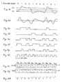
- Referring to Fig. 1 of the drawings, data recorded in a magnetic tape or a magnetic disk by a NRZ signal as transitions of magnetic polarity are reproduced by an inductive head in the form of an analog waveform (Fig. 1a). A digital data reproducing circuit differentiates the reproduced waveform to produce a differentiated signal having a waveform shown in Fig. 1b. Comparing the differentiated signal with a zero level line which is representative of AC zero volt, the reproducing circuit generates a digital peak detection signal as shown in Fig. 1c.
- When a magnetic recording medium has a magnetic defect such as a change in the density of magnetic powder or when electrical noise is introduced in a playback system from outside the system, there occurs false data usually called "drop-in" or the omission of data usually called "drop-out". In the light of this, the conventional reproducing circuit compares the amplitudes of the reproduced analog signal (Fig. 1a) with threshold levels +V and -V to output a positive and a negative detection signals as shown in Figs. 1d and 1e, respectively. The reproduced digital data signal (Fig. 1f) are such that data "1" appears when the positive or negative detection signal (Fig. 1d or 1e) has a high level at any of the positive- and negative-going edges of the peak detection signal (Fig. 1c).
- When externally derived noises g₂ and g₃ are superposed on the reproduced analog signal (Fig. 1a), the reproduced signal changes as shown in Fig. 1g. While the noise g₂ does not exceed the threshold level +V, the noise g₃ does exceed the threshold level -V. A problem with the prior art reproducing circuit is that it translates such a noise g₃ into data "1" and thereby produces a false digital signal, as shown in Fig. 1h.
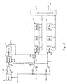
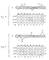
- Referring to Fig. 2, a digital data reproducing circuit embodying the present invention is shown and includes first and
second comparators 1 and 2, respectively. Thefirst comparator 1 produces a high level "H" when a reproduced analog signal a has a positive amplitude higher than a first positive threshold level +V₁, while the second comparator 2 produces "H" when the analog signal a has an amplitude lower than a negative threshold level -V₁. The outputs of the first andsecond comparators 1 and 2 are connected to the inputs of a peak detector 5. A differentiator 6 electrically differentiates the reproduced analog signal a. A third comparator produces "H" when the differentiated output of the differentiator 6 is positive. The output of thethird comparator 7 is also connected to the peak detector 5. The output of the peak detector 5 is coupled to a phase-locked loop circuit (PLL) 13. - The outputs of the first and
second comparators 1 and 2 are fed to an OR gate 8. Each of first andsecond shift registers 10 and 11 are implemented as a serial-in parallel-out shift register. Thefirst shift register 10 has a serial input connecting to thefirst comparator 1, while the second shift register 11 has a serial input connecting to the second comparator 2. ThePLL 13 outputs clock signal h the phase and frequency of which are synchronous to an output of the peak detector 5. The output of thePLL 13 is connected to shift clock inputs of the first andsecond shift registers 10 and 11. Parallel outputs of theshift registers 10 and 11 are conencted to adata discriminator 12 which produces reproduced digital data k. - The bit length required of each of the
shift registers 10 and 11 is more than the largest interval between consecutive data "1" produced by coding, plus 1 (one). In the above-stated recording system, for example, since the number of bits in which "0" continuously appears is three at maximum, the required bit length of theshift registers 10 and 11 is five or more bits. - Reference will be made to Figs. 3 and 5 for describing how data recorded in a magnetic tape by an ANSI X3B5 recording system are read out by the circuitry of Fig. 2 with the tape being driven in the forward and reverse directions, respectively.
- The
first comparator 1 produces a positive level detection signal c by detecting the portions of the reproduced analog signal a which are higher than the positive level +V₁. The second comparator 2 produces a negative level detection signal d by detecting the portions of the signal a which are lower than the negative level -V₁. The OR gate 8 ORs the outputs of thecomparators 1 and 2 to output an OR signal e. The differentiator 6 transforms the reproduced signal a into an analog differentiated signal b. Thethird comparator 7 produces a differentiated level detection signal f by comparing the signal b with zero volt. - The peak detector 5 monitors the positive and negative level signals c and d at the positive-going and negative-going edges of the differentiated level detection signal f. When any of the signals c and d has a level "H", the peak detector 5 outputs a level "H" having a predetermined pulse width to thereby produces a peak detection signal g. Hence, the positive-going edges of the peak detection signal g are representative of the timings of the positive and negative peaks of the reproduced signal a. Receiving the peak signal g, the
PLL 13 generates the clock signal h whose positive-going edges are phase-locked to those of the peak signal g. - One period of the clock signal h defines one bit cell, and each of the timing of the positive-going edges of the clock signal h is representative of the center of a bit cell. Data produced by sampling the positive level signal c and OR signal e at the positive-going edges of the clock signal h are sequentially stored in the shift registers 10 and 11, respectively. Specifically, the positive level detection signal c is stored in the
first shift register 10 at the positive-going edges of the clock h while being sequentially shifted. The data stored in theshift register 10 shows that the reproduced signal a has a positive peak in the associated bit cell. On the other hand, the OR signal e (OR of the positive level and negative level signals c and d) is stored in the second shift register 11 at the positive-going edges of the clock h while being sequentially shifted. The data stored in the shift register 11 indicates whether or not the signal a has a positive or negative peak exceeding the threshold level +V₁, or -V₁ in the associated bit cell. - As Fig. 4 indicates, when the magnetic tape is driven in the forward direction, the level signals are stored in the first and second shift registers 10 and 11 while being sequentially shifted in bit positions b₀, b₁, b₂ and so forth in this order. In this case, therefore, the level signal in the bit position b₁₀ is the level signal stored last with respect to time. When the content of the second shift register 11 is a low level "L", the
data discriminator 12 determines that the bit cell is data "0". - Let the description be continued with attention paid to the bit b₄ by way of example. In a reproduced waveform associated with the ANSI X3B5 recording system, the first peak appearing after a previous peak whose polarity is reverse to the first peak corresponds to data "1" during forward playback. The data discriminator 12 detects, on the basis of the content of bit 2b₄ of the shift register 11, that a candidate representative of a peak having an amplitude exceeding the threshold level +V₁ or -V₁, i.e., data "1" exists in the associated bit cell b₄. The data discriminator 12 also knows, on the bais of the content of bit 1b₄ of the
shift register 10, that the peak in that bit cell b₄ has negative polarity. - To determine whether or not the above-mentioned peak is data "1" or "0", the
data discriminator 12 checks the bits of the first and second shift registers 10 and 11 which precede the bit b₄, i.e., the bits 2b₃ to 2b₀ of the second register 11 to find a particular bit which has a level "H" and is closest to the b₄with respect to time. Then, thedata discriminator 12 determines the polarity of the particular bit by referencing the content of thefirst shift register 10, i.e., whether or not it is opposite to the polarity of the bit 1b₄. If the bit of interest is opposite in polarity to the bit 1b₄, thedata discriminator 12 determines that the bit b₄ is data "1"; if otherwise, it determines that the bit b₄ is data "0". More specifically, among the bits 2b₃ to 2b₀ of the second shift register 11, the bits 2b₃, 2b₂ and 2b₁ have a level "H" and it is the bit 2b₃ that is closest to the bit 2b₄ with respect to time. The bit 2b₃ of thefirst shift register 10 associated with the bit 2b₃ has a level "H" which is opposite to the polarity of the bit 1b₄. Hence, thedata discriminator 12 determines that the bit b₄ is data "1". - Next, concerning the bit b₇ which has a level "H" is the second register 11, whether it corresponds to the data "1" or "0" is determined on the basis of the contents of the bits b₃, b₄, b₅ and b₆ of the first and second shift registers 10 and 11. The content of the big 1b₇ of the
first register 10 indicates that the peak of the reproduced analog signal a existing in this bit cell has negative polarity. The contents of the second register 11 show that the bit 2b₄ is the bit which has a level "H" and closest to the bit 2b₇. Further, the content of the bit 1b₄ of thefirst register 10 shows that the peak of the signal a existing in this bit cell has negative polarity. Since the bits 1b₇ and 1b₄ have the same polarity, it is determined that the bit b₇ is data "0". By the same procedure, it is determined that the bit b₈ is data"1" and that the bit b₁₀ is data "0". - Fig. 6 indicates the procedure for reproducing the digital data k out of the analog signal a by driving the magnetic tape reproduced in the reverse direction. As shown in Fig. 5, the analog signal a produced by the reverse playback has a waveform opposite to the waveform of Fig. 3 with respect to time and amplitude, due to the magnetism reciprocity principle. The waveform associated with the reverse playback, contrary to the waveform associated with the forward playback, is such that the last peak of the same polarity after a peak whose polarity is reverse to the last peak corresponds to data "1", due to the magnetism reciprocity principle. Concerning the bit b₀, for example, the
data discriminator 12 recognizes that a peak whose amplitude exceeds +V₁ or -V₁ exists in the signal a within the bit cell b₀, on the basis of the content of a bit 2b₀ of the second shift register 11. The data discriminator 12 also determines that the peak existing in the bit cell b₀ has positive polarity, based on the content 1b₀ of thefirst register 10. - To see if the peak in the bit b₀ is data "1" or "0", the
data discriminator 12 checks the bits b₁, b₂, b₃ and b₄ of the shift registers 10 and 11 which follow the bit b₀ of interest, i.e., it searches for particular one of the bits 2b₁ to 2b₄ which has a level "H" and is closest to the bit b₀ with respect to time. Then, the data discriminator 12 references the content of thefirst register 10 to determine the polarity of the peak of the particular bit. If the determined polarity is opposite to the polarity of the bit 1b₀, the data discriminator 12 regards that the bit b₀ is data "1", if otherwise, it regards that the bit b₀ is data "0". More specifically, among the bits 2b₁ to 2b₄ of the second shift register 11, the bits 2b₂ and 2b₃ have a level "H" and it is the bit 2b₂ that is closest to the bit 2b₀. The bit 1b₂ of thefirst register 10 which corresponds to the bit 2b₂ has a level "H" which is opposite in polarity to the bit 1b₀. Consequently, thedata discriminator 12 determines that the bit b₀ is data "1". In the same manner, it determines that the bit b₂ is data "1". - Whether the bit b₃ corresponds to data "1" or "0" is dependent on the contents of the bits b₄, b₅ b₆ and b₇ of the shift registers 10 and 11. The content of the bit 1b₃ of the
first register 10 indicates that the peak of the signal a existing in this bit cell b₃ has negative polarity. The contents of the bits 2b₄ to 2b₇ of the second register 11 show that the bit having a level "H" and closest to the bit 2b₃ is the bit b₆. Further, the content of the bit 1b₆ of thefirst register 10 shows that the peak of the signal a existing in this bit cell b₆ has a peak negative polarity. Since the bits 1b₃ and 1b₆ have the same polarity, it is determined that the bit b₃ is data "0". By the same procedure, the bits b₆ and b₉ are determined to be data "1" and the bit b₇ and b₈ are data "0", respectively. - The data discriminator 12 may be implemented by a microprocessor capable of performing the above operations. If desired, the
data discriminator 12 may be provided with a table individually associated with the bits of the first and second shift registers 10 and 11, and may be so constructed to determine that a bit bi is data "1" when any of the combinations shown in Table 1 is satisfied. In such a case, thedata discriminator 12 may be constituted by a ROM or a programmable logic array for implementing rapid data discrimination.Table 1 2ND REGISTER 11 1ST REGISTER 102bi-4 2bi-3 2bi-2 2bi-1 2bi 1bi-4 1bi-3 1bi-2 1bi-1 1bi FORWARD PLAYBACK H H L H H H H L H L H L H H L H H L H L L H L H H L L H H L H L L L H L H H L L L H H L 2ND REGISTER 11 1ST REGISTER 102bi 2bi+1 2bi+2 2bi+3 2bi+4 1bi 1bi+1 1bi+2 1bi+3 1bi+4 REVERSE PLAYBACK H H H L H H L H H L H H L H L H L H H L L H H L H L L H L H H L L L H H L H L L L H L H - Fig. 7 shows a second embodiment of the present invention. In the figure, similar components or structural elements are designated by the same reference numerals, and redundant description will be avoided for simplicity.
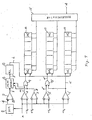
- In Fig. 7, a
first comparator 1′ produces a level "H" when the positive amplitude of the reproduced analog signal a is higher than a threshold level +V₂, while a second comparator 2′ produces a level "H" when the negative amplitude of the signal a is lower than a threshold level -V₂. The outputs of thecomparators 1′ and 2′ are connected to a first OR gate 8′. The threshold levels +V₂ and -V₂ are smaller than the threshold levels +V₁ and -V₁ used in the first embodiment with respect to the absolute value. - A fourth comparator 3 produces "H" when the positive amplitude of the signal a ia higher than a second threshold level +V₃, while a
fifth comparator 4 produces "H" when the negative amplitude of the signal a is lower than a second threshold level -V₃. The outputs of thecomparators 3 and 4 are conencted to the peak detector 5 and a second ORgate 9. The threshold levels +V₃ and -V₃ are greater than the threshold levels +V₁ and -V₁ with respect to the absolute value. - A
third shift register 14 is also implemented as a serial-in parallel-out shift register and has a serial input connecting to the output of the second ORgate 9. The output of thePLL 13 is connected to the shift clock h inputs of the shift registers 10, 11 and 14. The parallel outputs ofshift registers data discriminator 12′. The bit length required of each of the shift registers 10, 11 and 14 is more than twice the largest interval between successive "1" produced by coding, plus 1 (one). For example, in the case of a recording system adopting a coding principle which allows "0" to continuously appear in only three bits at maximum, the required bit length will be nine or more bits. - As shown in Fig. 8, the
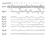
first comparator 1′ produces a positive low-level detection signal c′ (Fig. 8c′) by detecting the portions of the reproduced signal a which are higher than the first level +V₂. The second comparator 2′ produces a negative low-level detection signal d′ (Fig. 8d′) by detecting the portions of the signal a which are lower than the first level -V₂. The fourth andfifth comparators 3 and 4 produce respectively positive and negative high-level signal l and m, as shown in Figs. 8l and m. - The
comparator 7 shown in Fig. 7 outputs a signal shown in Fig. 8f by comparing the differentiated signal b with zero volt. The peak detector 5 produces a peak detection signal g′ shown in Fig. 8g′ on the basis of the outputs of the third tofifth comparators PLL 13 produces a clock signal h the positive-going edges of which are phase-locked to those of the signal g′, as shown in Fig. 8h. - The
first shift register 10 stores the positive low-level detection signal c′ at the positive-going edges of the clock h while sequentially shifting it. By referencing an output of theshift register 10, thedata discriminator 12′ determines whether a peak existing in the bit cell has positive polarity or negative polarity. The second shift register 11 stores an output e′ of the OR gate 8′ (OR of the positive and negative low-level signals c′ and d′) at the positive-going edges of the clock h while sequentially shifting it. Based on the signal e′, thedata discriminator 12′ determines whether the amplitude of the peak in the bit cell exceeds the first level +V₂ or -V₂. - The
third shift register 14 stores the output of the OR gate 9 (OR of the positive and negative high-level detection signals l and m) at the positive-going edges of the clock h while sequentially shifting it. This signal allows thedata discriminator 12′ to see if the amplitude of the peak existing in the bit cell exceeds the second level +V₃ or -V₃. - The data discriminator 12′ determines a bit cell wherein the peak of the signal a exceeds the second level +V₃ or -V₃ to be data "1", on the basis of the contents of the
third shift register 14. The data discriminator 12′ also determines, on the basis of the contents of the second and third shift registers 11 and 14, that a bit cell wherein the peak has an amplitude exceeding the first level +V₂ or -V₂ but short of the second level +V₃ or -V₃ is a candidate of date "1". Further, thedata discriminator 12′ regards that a bit cell wherein the content of the second register 11 is "L" is data "0". - In the example shown in Fig. 9, the signal a has a peak P₂ which exceeds the first level -V₂ but is short of the second level -V₃. In this instance, positive peaks P₁ and P₃ each exceeding the second level +V₃ exist before and after the peak P₂ with respect to time. In general, digital magnetic recording is accomplished by associating the reversal points of polarity with data so that a transition from S to N, for example, is necessarily followed by a transition from N to S. Henve, a recovered analog signal associated with such transitions alternates. It follows that the peak P₂ can be regarded as a signal representative of data "1" the amplitude of which has been deteriorate.
- As stated above, in the illustrative embodiment, the data reproducing circuit stores the transitions of reproduced amplitude on a bit cell basis so that even a peak which satisfies the above-described conditions but does not exceed the second level V₃ is picked up as data "1" by referencing the preceding and following amplitude data as well as polarity data.
- The decision on the bit bi as to "1"/"0" will be described in more detail. The contents of the bits bi of the first to third shift registers 10, 11 and 14 indicate that the peak P₂ is representative of a negative pulse whose amplitude is too small for the pulse enough to represent data "1". To determine whether the bit bi is data "1" or noise, the bits preceding and following it with respect to time are observed. On the basis of the contents stored in the
bits 1i-3 of the shift registers 10, 11 and 14, it is seen that the peak P₁ has a sufficiently large positive amplitude. It is also seen that a signal having a sufficiently large positive amplitude exists in the bits bi+4 also, based on the contents of the shift registers 10, 11 and 14. The data discriminator 12′ therefore regards the peak in the bit bi as data "1" and produces digit data k. - Fig. 10 shows another example of the reproduced signal a useful for understanding the above procedure. In the figure, let the bit bi be the bit of interest. The contents of the bits bi of the
respective shift registers data discriminator 12′ determines that the peak P₅ is noise occurred between the peaks P₄ and P₆ and thereby produces data "0". - In this manner, the
data discriminator 12′ references those bits of the shift registers 10, 11 and 14 which are associated with a point where a signal exists and, when predetermined conditions for decision are satisfied, produces data "1". This prevents a peak representative of data "1" but having somewhat lowered amplitude from being neglected. - Fig. 11, shows a third embodiment of the present invention. In the figures, similar components and structural elements are designated by the same reference numerals, and redundant description will be avoided for simplicity.
- In Fig. 11, the output c′ of the
first comparatos 1′, the output e′ of the first OR gate 8′ and the output of the second ORgate 9 are connected to D terminals of first, second and third D type flip-flops second peak detector 20 is supplied with the outputs c′, d′ and f of the first, second andthird comparators 1′, 2′ and 7. Thepeak detector 20 has an output connecting to clock terminals CK of slip-flops PLL 13 produces a clock signal h′ the negative-going edges of which are synchronous to the positive-going edges of the output g′ of the peak detector 5. Specifically, the negative-going edges of the clock h′ are associated with the peaks of the reproduced signal a, and one period between consecutive positive-going edges defines one bit cell. The clock h′ from thePLL 13 is fed to a one-shot circuit 18. The one-shot circuit 18 produces an output o which is slightly delayed in phase relative to the positive-going edges of the output h′ of thePLL 13. The signal o being applied to reset terminals RST of the flip-flops flops - The parallel outputs of the
first shift register 10 are connected to adata discriminator 12˝ by way of an Exclusive-OR (EX-OR)gate group 19. The EX-OR gates constituting thegroup 19 have one input connecting to the parallel outputs of thefirst shift register 10 except for the center bit bi of the latter, and the other input connecting to the center bit bi. In this configuration, each EX-OR gate produces a level "H" only when data different from the data of the bit bi of interest is applied thereto. - How each level signal is taken in will be described with reference also made to Fig. 12. The second D type flip-
flop 22 holds the output e′ of the first OR gate 8′ at positive-going edges of the output n of thepeak detector 20, thereby producing a signal shown in Fig. 12q. The second shift register 11 takes in the signal n in synchronism with positive-going edges of the clock h′ (trailing edge of bit cell) while sequentially shifting it. Based on the content of the shift register 11 thediscriminator 12˝ can determine whether the peak has an amplitude which exceeds the first level V₂. - The third D-type flip-
flop 23 holds the output of the second OR gate 9 (i.e., OR of the positive high-level detection signal l and negative high-level detection signal m) at the positive-going edges of the output n of thepeak detector 20, thereby producing a signal shown in Fig. 12r. Thethird shift register 14 takes in the signal r in synchronism with the positive-going edges of the clock h′ while sequentially shifting it. Based on the content of theshift register 14, thediscriminator 12˝ can determine whether the peak has an amplitude which exceeds the second level V₃. - The first D type flip-
flop 21 takes in the holds the positive low-level detection signal c′ at positive-going edge of the output n of thepeak detector 20, thereby producing a signal p shown in Fig. 12p. Thefirst shift register 10 takes in the signal p at a positive-going edge of the clock h′ while shifting it. The data discriminator 12˝ determines whether the peak is positive or negative on the basis of an output of theshift register 10. TheEX-OR gate group 19 compares the center bit bi of thefirst shift register 10, i.e., the bit to be decided as to "1"/"0" with the other bits, producing "0" if they compare equal in polarity and "1" if otherwise. This allows thedata discrimination 12˝ to readily determine whether or not the center bit bi and the other its of theshift register 10 are opposite in polarity. The data discriminator 12˝ is operated in the same manner as described with reference to Figs. 9 and 10, and details thereof will not be described to avoid redundancy. - In summary, it will be seen that the present invention provides an interlligent data reproducing circuit which reduces the loads on error checking and error correcting circuits of the kind using a parity check code or similar redundant code, thereby reproducing data efficiently and accurately. These advantages of the present invention are derived from a unique procedure wherein a characteristic of a reproduced analog signal waveform is stored in the form of a digital value and, when a signal which is difficult to decide as to data/noise appears, amplitudes around such a signal are feferenced to reproduce more correct data.
Claims (5)
a first comparator for determining that a positive amplitude of a reproduced analog signal exceeds a positive first level;
a second comparator for determining that a negative amplitude of said reproduced analog signal exceeds a negative first level;
a clock generating circuit for generating a clock signal phase-locked to timings of positive and negative peaks of said reproduced analog signal;
a first shift register for taking in an output of said first comparator or said second comparator in response to said clock signal to shift and store said output;
a second shift register for taking in OR signal of outputs of said first comparator and said second comparator in response to said clock signal to shift and store said OR signal; and
a discriminator for producing digital data from parallel outputs of said first shift register and said second shift register.
a differentiator for producing a differentiated signal by differentiating said reproduced analog signal;
a third comparator for producing a differentiated level detection signal by detecting positive and negative levels of said differented signal;
a peak detector for producing a peak detection signal on the basis of said differentiated level detection signal; and
a phase-locked loop for generating said clock signal in synchronism with said peak detection signal.
a fourth comparator for determining that a positive amplitude of said reproduced analog signal exceeds a second positive level which is higher than said first positive level;
a fifth comparator for determining that a negative amplitude of said reproduced analog signal exceeds a second negative level which is lower than said first negative level; and
a third shift register for taking in OR signal of outputs of said fourth comparator and said fifth comparator in response to the clock signal to shift and store said OR signal;
said discriminator producing the digital data by referencing a parallel outout of said third shift register as well as the outputs of said first and second shift registers.
a first flip-flop receiving an output of said first comparator and feeding its output to said first shift register;
a second flip-flop receiving said OR signal of said first and second comparators and feeding its output to said second shift register; and
a one-shot circuit for resetting said first and second flip-flops in response to said clock signal.
Applications Claiming Priority (8)
| Application Number | Priority Date | Filing Date | Title |
|---|---|---|---|
| JP63129452A JPH0736206B2 (en) | 1988-05-28 | 1988-05-28 | Digital data reproduction circuit |
| JP129452/88 | 1988-05-28 | ||
| JP158743/88 | 1988-06-27 | ||
| JP15874388A JPH029008A (en) | 1988-06-27 | 1988-06-27 | Data reproducing circuit |
| JP63222291A JPH0738244B2 (en) | 1988-09-07 | 1988-09-07 | Data reproduction circuit |
| JP222292/88 | 1988-09-07 | ||
| JP222291/88 | 1988-09-07 | ||
| JP63222292A JPH0738245B2 (en) | 1988-09-07 | 1988-09-07 | Data reproduction circuit |
Publications (3)
| Publication Number | Publication Date |
|---|---|
| EP0344669A2 true EP0344669A2 (en) | 1989-12-06 |
| EP0344669A3 EP0344669A3 (en) | 1991-08-07 |
| EP0344669B1 EP0344669B1 (en) | 1994-08-17 |
Family
ID=27471456
Family Applications (1)
| Application Number | Title | Priority Date | Filing Date |
|---|---|---|---|
| EP89109617A Expired - Lifetime EP0344669B1 (en) | 1988-05-28 | 1989-05-29 | Digital data reproducing circuit for a magnetic recording apparatus |
Country Status (3)
| Country | Link |
|---|---|
| US (1) | US5089821A (en) |
| EP (1) | EP0344669B1 (en) |
| DE (1) | DE68917526T2 (en) |
Cited By (2)
| Publication number | Priority date | Publication date | Assignee | Title |
|---|---|---|---|---|
| EP0399513A1 (en) * | 1989-05-24 | 1990-11-28 | Sony Corporation | Pit pattern detecting method |
| EP2921922A1 (en) * | 2014-03-17 | 2015-09-23 | Rockwell Automation Limited | Method and apparatus for monitoring a signal |
Families Citing this family (5)
| Publication number | Priority date | Publication date | Assignee | Title |
|---|---|---|---|---|
| US5231544A (en) * | 1990-01-29 | 1993-07-27 | Hitachi, Ltd. | Method and apparatus for signal detection in a magnetic recording and reproducing apparatus |
| JPH05234273A (en) * | 1990-11-30 | 1993-09-10 | Hitachi Ltd | Device for evaluating signal waveform and magnetic disk device |
| US5627846A (en) * | 1995-04-19 | 1997-05-06 | Eastman Kodak Company | Drop-out location detection circuit |
| US5615223A (en) * | 1995-04-19 | 1997-03-25 | Eastman Kodak Company | PPM decoder utilizing drop-out location information |
| US7683577B2 (en) * | 2005-03-07 | 2010-03-23 | O2Micro International Limited | Battery state monitoring circuitry with low power consumption during a stand-by-state of a battery pack |
Citations (1)
| Publication number | Priority date | Publication date | Assignee | Title |
|---|---|---|---|---|
| US4626933A (en) * | 1983-08-18 | 1986-12-02 | Amcodyne Incorporated | Method and apparatus for qualifying data |
Family Cites Families (2)
| Publication number | Priority date | Publication date | Assignee | Title |
|---|---|---|---|---|
| JPS4957759A (en) * | 1972-10-02 | 1974-06-05 | ||
| US3821716A (en) * | 1973-03-05 | 1974-06-28 | Honeywell Inf Systems | Method and apparatus for recovering data in an nrzi recording system |
-
1989
- 1989-05-29 EP EP89109617A patent/EP0344669B1/en not_active Expired - Lifetime
- 1989-05-29 DE DE68917526T patent/DE68917526T2/en not_active Expired - Fee Related
- 1989-05-30 US US07/358,956 patent/US5089821A/en not_active Expired - Lifetime
Patent Citations (1)
| Publication number | Priority date | Publication date | Assignee | Title |
|---|---|---|---|---|
| US4626933A (en) * | 1983-08-18 | 1986-12-02 | Amcodyne Incorporated | Method and apparatus for qualifying data |
Non-Patent Citations (1)
| Title |
|---|
| IEEE TRANSACTIONS ON MAGNETICS, vol. MAG-23, no. 5, (Part II of two parts), September 1987, pages 3675-3677, New York, NY, US; Y. OUCHI et al.: "A new signal detection method with two slice levels" * |
Cited By (4)
| Publication number | Priority date | Publication date | Assignee | Title |
|---|---|---|---|---|
| EP0399513A1 (en) * | 1989-05-24 | 1990-11-28 | Sony Corporation | Pit pattern detecting method |
| US5136564A (en) * | 1989-05-24 | 1992-08-04 | Sony Corporation | Pit pattern detecting apparatus and method |
| EP2921922A1 (en) * | 2014-03-17 | 2015-09-23 | Rockwell Automation Limited | Method and apparatus for monitoring a signal |
| US9331682B2 (en) | 2014-03-17 | 2016-05-03 | Rockwell Automation Limited | Method and apparatus for monitoring a signal |
Also Published As
| Publication number | Publication date |
|---|---|
| EP0344669A3 (en) | 1991-08-07 |
| EP0344669B1 (en) | 1994-08-17 |
| DE68917526T2 (en) | 1995-02-09 |
| DE68917526D1 (en) | 1994-09-22 |
| US5089821A (en) | 1992-02-18 |
Similar Documents
| Publication | Publication Date | Title |
|---|---|---|
| US4520346A (en) | Method and apparatus for encoding an NRZI digital signal with low DC component | |
| US4499454A (en) | Method and apparatus for encoding a digital signal with a low DC component | |
| EP0673028B1 (en) | Recording medium, signal recording apparatus thereof, and signal reproducing apparatus thereof | |
| US4833471A (en) | Data processing apparatus | |
| JPH06195893A (en) | Method and device for data recording | |
| US6492915B2 (en) | Method for recording information, method for reproducing information, and information recording apparatus | |
| US5406569A (en) | Error correcting apparatus for digital data and digital synchronizing detecting apparatus | |
| GB2105152A (en) | Method and apparatus for processing binary data | |
| EP0310330A2 (en) | Digital signal recording/reproducing apparatus | |
| JPH0714145B2 (en) | Information conversion method | |
| US4577180A (en) | Digital data converting method and apparatus thereof | |
| US5625632A (en) | Magnetic disk drive including a data discrimination apparatus capable of correcting signal waveform distortion due to intersymbol interference | |
| EP0344669A2 (en) | Digital data reproducing circuit for a magnetic recording apparatus | |
| EP0739009A2 (en) | PPM decoder utilizing drop-out location information | |
| EP0430457B1 (en) | Method and apparatus for qualifying data pulses in a raw data signal produced by a magnetic transducer | |
| JP3309334B2 (en) | Data channel | |
| US4549167A (en) | Method of encoding and decoding binary data | |
| US5231544A (en) | Method and apparatus for signal detection in a magnetic recording and reproducing apparatus | |
| US5175655A (en) | Method and apparatus for verifying a signal recorded in an encoded form on a medium | |
| US4845574A (en) | Apparatus for recording and reproducing digital signals on magnetic tape | |
| US5812560A (en) | Magnetic disk certifier | |
| EP0196034B1 (en) | Apparatus for recording and reproducing digital signal | |
| JPH0738244B2 (en) | Data reproduction circuit | |
| JPH01300408A (en) | Digital data reproducing circuit | |
| KR100339347B1 (en) | Data recovering device for dvcr |
Legal Events
| Date | Code | Title | Description |
|---|---|---|---|
| PUAI | Public reference made under article 153(3) epc to a published international application that has entered the european phase |
Free format text: ORIGINAL CODE: 0009012 |
|
| 17P | Request for examination filed |
Effective date: 19890622 |
|
| AK | Designated contracting states |
Kind code of ref document: A2 Designated state(s): DE FR GB |
|
| PUAL | Search report despatched |
Free format text: ORIGINAL CODE: 0009013 |
|
| AK | Designated contracting states |
Kind code of ref document: A3 Designated state(s): DE FR GB |
|
| 17Q | First examination report despatched |
Effective date: 19930128 |
|
| GRAA | (expected) grant |
Free format text: ORIGINAL CODE: 0009210 |
|
| AK | Designated contracting states |
Kind code of ref document: B1 Designated state(s): DE FR GB |
|
| REF | Corresponds to: |
Ref document number: 68917526 Country of ref document: DE Date of ref document: 19940922 |
|
| ET | Fr: translation filed | ||
| PGFP | Annual fee paid to national office [announced via postgrant information from national office to epo] |
Ref country code: DE Payment date: 19950522 Year of fee payment: 7 |
|
| PGFP | Annual fee paid to national office [announced via postgrant information from national office to epo] |
Ref country code: GB Payment date: 19950523 Year of fee payment: 7 |
|
| PLBE | No opposition filed within time limit |
Free format text: ORIGINAL CODE: 0009261 |
|
| STAA | Information on the status of an ep patent application or granted ep patent |
Free format text: STATUS: NO OPPOSITION FILED WITHIN TIME LIMIT |
|
| 26N | No opposition filed | ||
| PG25 | Lapsed in a contracting state [announced via postgrant information from national office to epo] |
Ref country code: GB Effective date: 19960529 |
|
| GBPC | Gb: european patent ceased through non-payment of renewal fee |
Effective date: 19960529 |
|
| PG25 | Lapsed in a contracting state [announced via postgrant information from national office to epo] |
Ref country code: DE Effective date: 19970201 |
|
| PGFP | Annual fee paid to national office [announced via postgrant information from national office to epo] |
Ref country code: FR Payment date: 19970529 Year of fee payment: 9 |
|
| PG25 | Lapsed in a contracting state [announced via postgrant information from national office to epo] |
Ref country code: FR Free format text: LAPSE BECAUSE OF NON-PAYMENT OF DUE FEES Effective date: 19980531 |
|
| REG | Reference to a national code |
Ref country code: FR Ref legal event code: ST |