EP0342639A2 - Microlithographic apparatus - Google Patents
Microlithographic apparatus Download PDFInfo
- Publication number
- EP0342639A2 EP0342639A2 EP89108854A EP89108854A EP0342639A2 EP 0342639 A2 EP0342639 A2 EP 0342639A2 EP 89108854 A EP89108854 A EP 89108854A EP 89108854 A EP89108854 A EP 89108854A EP 0342639 A2 EP0342639 A2 EP 0342639A2
- Authority
- EP
- European Patent Office
- Prior art keywords
- stage
- monolithic
- electro
- sub
- monolithic stage
- Prior art date
- Legal status (The legal status is an assumption and is not a legal conclusion. Google has not performed a legal analysis and makes no representation as to the accuracy of the status listed.)
- Granted
Links
Images

Classifications
-
- G—PHYSICS
- G03—PHOTOGRAPHY; CINEMATOGRAPHY; ANALOGOUS TECHNIQUES USING WAVES OTHER THAN OPTICAL WAVES; ELECTROGRAPHY; HOLOGRAPHY
- G03F—PHOTOMECHANICAL PRODUCTION OF TEXTURED OR PATTERNED SURFACES, e.g. FOR PRINTING, FOR PROCESSING OF SEMICONDUCTOR DEVICES; MATERIALS THEREFOR; ORIGINALS THEREFOR; APPARATUS SPECIALLY ADAPTED THEREFOR
- G03F7/00—Photomechanical, e.g. photolithographic, production of textured or patterned surfaces, e.g. printing surfaces; Materials therefor, e.g. comprising photoresists; Apparatus specially adapted therefor
- G03F7/70—Microphotolithographic exposure; Apparatus therefor
- G03F7/70691—Handling of masks or workpieces
- G03F7/70716—Stages
-
- H—ELECTRICITY
- H01—ELECTRIC ELEMENTS
- H01L—SEMICONDUCTOR DEVICES NOT COVERED BY CLASS H10
- H01L21/00—Processes or apparatus adapted for the manufacture or treatment of semiconductor or solid state devices or of parts thereof
- H01L21/67—Apparatus specially adapted for handling semiconductor or electric solid state devices during manufacture or treatment thereof; Apparatus specially adapted for handling wafers during manufacture or treatment of semiconductor or electric solid state devices or components ; Apparatus not specifically provided for elsewhere
- H01L21/68—Apparatus specially adapted for handling semiconductor or electric solid state devices during manufacture or treatment thereof; Apparatus specially adapted for handling wafers during manufacture or treatment of semiconductor or electric solid state devices or components ; Apparatus not specifically provided for elsewhere for positioning, orientation or alignment
- H01L21/682—Mask-wafer alignment
Definitions
- This invention relates to microlithographic instruments and more particularly to electro-magnetic alignment apparatus which is particularly adapted, among other possible uses, for use in aligning the wafer in a microlithography system.
- My own patent No. 4,506,204 shows electro-magnetic alignment apparatus which includes at least three magnet assemblies mounted in spaced relationship, at least three coil assemblies mounted to pass through the high flux region of the magnet assemblies, means for connecting the coil assemblies to form a rigid structure, and means for controlling the supply of current to the coils so that the structure can be moved selectively in three degreees of freedom.
- My present contribution to the art is a new alignment apparatus, which is an improvement over such known systems.
- an electro-magnetic alignment apparatus which includes a monolithic stage, a sub-stage, an isolated reference structure, force actuators interposed between the monolithic stage and the sub-stage for suspending and positioning the monolithic stage in space, control means for controlling the position of the monolithic stage, sensors mounted between the isolated reference structure and the monolithic stage for sensing the position of the monolithic stage and outputting a signal to the control means.
- the control means is constructed and arranged to compare the sensed position of the monolithic stage with a commanded stage position and output an error signal to the force actuators.
- the apparatus further includes means for controlling the position of the sub-stage to follow the approximate position of the monolithic stage.
- the force actuators include a coil component mounted on the sub-stage and a separate non-contacting magnet structure mounted on the monolithic stage.
- the sensors include laser gage sensors for three degrees of freedom and short range non-contact electro-optical sensors for three different degrees of freedom of the monolithic stage.
- the means for controlling the position of the sub-stage includes at least two separate non-contact sensors, and two linear servo motors operatively responsive to the non-contact sensors.
- control means are constructed and arranged to provide an acceleration feed forward signal which combines with the sensed positon signal to output a modified control signal to the force actuators.
- the control means are also constructed and arranged to provide an acceleration feed forward signal which combines with the signals from the non-contact sensors to output a modified control signal to the linear servo motors.
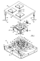
- the new and improved electro-magnetic alignment devise comprises a monolithic stage 10, an X-Y sub-stage 12 and an isolated reference structure 14, as shown in Fig. 1.
- the X-Y sub-stage 12 is a conventional X-Y mechanically guided sub-stage, which is servo driven to follow the approximate position of the monolithic stage. It could employ anti-friction bearings such as, for example, ball bearings or roller bearings as ways. Air bearings could also be used, but they are unnecessary. As a result the instrument could operate in a vacuum, if desired. Actually the entire alignment device could be arranged to operate in a vacuum for some installations, if desired.
- the sub-stage 12 includes a base plate 16 mounted on the ground, as indicated at 18, and a movable frame 20.
- the frame 20 is movable back and forth in the X direction, as indicated by arrow 22, by means of a linear servo motor 24.
- a deck member 26 is mounted on the frame 20 for back and forth movement in the Y direction, as indicated by arrow 28, by means of a linear servo motor 30 provided for the purpose.
- Other suitable drive mechanisms could be employed instead of the linear servo motors 24 and 30 such as, for example, ball screws, rotary motors or the equivalent.
- the bearings and drive means for the sub-stage 12 does not have to be very precise. It just has to be capable of reasonable acceleration velocities. As a result it can be relatively inexpensive and more compact than would be necessary if a planar force motor was employed, for example.
- the monolithic stage 10 includes a block member 32, which caries a wafer chuck 34, that supports a wafer 35.
- This compact, precision, monolithic stage is suspended in space with its position controlled in six degrees of freedom by high performance servos using short stroke, non-contact electro-magnetic force actuators.
- Four flat coil actuators, indicated at 36, are provided each of which include a flat coil component 38 mounted on the X-Y sub-stage 12 and a separate non-contacting high strength permanent magnet 40 mounted on the monolithic stage 10.
- Fig. 3 illustrates four flat coil actuators, it would be possible to operate with a minimum of three such actuators. These actuators provide for movement of the monolithic stage 10 in three degrees of freedom. That is, two actuators provide for movement in the X direction as indicated by arrows 42 and the other two actuators provide for movement in the Y direction as indicated by arrows 44.
- the monolithic stage is caused to rotate by driving all of the actuators simultaneously.
- Each of which include a cylindrical coil component mounted on the X-Y sub-stage 12 and a separate non-contacting high strength permanent magnet mounted on the monolithic stage 10.
- the flat coil actuators it is preferable to mount the coil component on the X-Y sub-stage 12 and the magnet on the monolithic stage 10, but it is also possible to reverse these elements. While it is possible to employ a minimum of three focus actuators, four is preferable.
- These focus actuators 46 provide an additional three degrees of freedom to the monolithic stage 10 as illustrated by the arrows 47. That is, the monolithic stage can be tilted as desired by the selection of the particular pair of actuators activated.
- the monolithic stage can be raised or lowered with respect to the X-Y sub-stage.
- the clearance between the two stages is generally maintained at a range of the order of about 1/32 inch.
- the use of flat coil and voice coil-type actuators as described is desirable because this configuration facilitates assembly and disassembly. That is, the monolithic stage can literally be lifted off the sub-stage along the "Z" axis. An all voice coil configuration is also practical.
- any missalignment between the monolithic stage 10 and the sub-stage 12 is measured by non-contact sensor assemblies, two being indicated at 48 near the center of the sub-stage and their mating portions being indicated at 48′ on the underside near the center of the monolithic stage.
- Two individual sensors or one combined sensor can be use to measure the X and Y positions. The output of these sensors is electronically amplified and fed back to the servo motors 24 and 30 to cause the sub-stage to approximately follow the motion of the monolithic stage and maintain alignment of the force actuators, as will be described more fully hereinafter.
- Any suitable type of non-contact short range sensors may be used such as a solid state emitter and split photodiode detector, a capacitance gage, or an LVDT, for example.
- the X-Y distance or position of the sub-stage with respect to the monolithic stage is what is important. The vertical distance or angular relationship between the two stages does not need to be sensed by these sensors.
- the monolithic stage is mounted on the sub-stage, in operation, the monolithic stage is actually floating in space above the substage, with its position controlled by the electro-magnetic force of the actuators. As long as the actuator coils remain in the magnetic field of their associated magnet structures, and do not contact those structures, then the position of the monolithic stage is unaffected by the position of the sub-stage.
- the instrument can be operated with extended motion in a vertical plane.
- the use of a counterforce device on the vertical axis of the sub-stage may be necessary in some installations.
- the isolated reference structure 14 comprises a support member 50, which is mounted on the ground 18 by means of isolators or springs 52.
- the support member carries an imaging optical system 54 and outer loop focus sensors 56.
- imaging optical systems could be employed such as, an exposing tool, an inspection tool or an electron beam, for example.
- a separate set of sensors 56 are mounted near the imaging optics 54, which look at several points directly on the surface of the wafer 35. These sensors are used to follow the wafer surface, which may not be flat. These sensors provide fine measurement, but they do not need to be as fast as the inner loop sensors which will be described hereinafter. Any suitable type of non-contact sensor may be employed sure as air gages, a cap gage or other type of optic sensor, for example.
- the instrument is provided with at least three inner loop electro-optical focus sensors 58 mounted on the corners of the monolithic stage 10 and three corresponding flats 60 mounted on the underside of the support number 50.
- the tilt position of the monolithic stage is sensed by these short range, non-contact, electro-optical sensors in three degrees of freedom.
- a beam is reflected off the mirror surface of the flats 60, and if the mirror moves closer or away a signal moves on a little cell to thereby sense small motion changes between the corners of the monolithic stage and the three flats.
- Other suitable types of sensors could be used such as a cap gage, for example.
- At least three laser gage plane mirror interferometers 62 are used to sense the positon of the monolithic stage d 10 in three degrees of freedom, X-Y and theta.
- the laser gages 62 depend from the support number 50 to a location adjacent the sides 64 of the block member 32.
- the sides 64 form mirrors by virtue of reflective coatings or by actual mirrors being mounted thereon. That is, the interferometers direct beams onto the sides to sense the X-Y and theta motion of the monolithic stage.
- Theta is a measure of the rotation in the plane.
- FIG. 2 shows this in more detail.
- One of the six degree systems is illustrated for purposes of clarity; ie the X system.
- a computer or profile generator 66 is used.
- the profile generator or commander is programed to know in advance the X-position where the monolithic stage is supposed to be.
- a summing junction 68 receives an X-position signal from the profile generator 66 and fromt he interferometer position sensor 62.
- the error output from the summing junction 68 passes through a servo compensation block 70 to a summing junction 72.
- the servo compensation block serves as an electrical network stabilizing system.
- a signal corresponding to the acceleration and feed forward position is outputted from the profile generator 66 to the summing junction 72.
- the output from the summing junction 72 passes through amplifier means 74 to drive the actuator 36.
- the signal from the sensor assembly 48 is directed through a servo compensation block 76 to a summing junction 78.
- the servo compensation block 76 serves as an electrical network stabilizing system similar to the compensation block 70.
- An acceleration and feed forward position signal from the profile generator 66 is also directed to the summing junction 78.
- the output from this summing junction is passed through amplifier means 80 to the linear servo motor actuator 24.
- the present invention does indeed provide a new and improved microlithographic instrument wherein the position of the monolithic stage is unaffected by vibration in the sub-stage, thereby permitting the sub-stage to be of a lower cost design, mounted without isolation from ground vibration. All the reaction loads from both the monolithic stage and the sub-stage are transmitted directly to the ground, and therefore do not disturb the isolated structure to which the position of the monolithic stage is electro-optically referenced.
Landscapes
- General Physics & Mathematics (AREA)
- Engineering & Computer Science (AREA)
- Physics & Mathematics (AREA)
- Microelectronics & Electronic Packaging (AREA)
- Manufacturing & Machinery (AREA)
- Computer Hardware Design (AREA)
- Condensed Matter Physics & Semiconductors (AREA)
- Power Engineering (AREA)
- Exposure And Positioning Against Photoresist Photosensitive Materials (AREA)
- Container, Conveyance, Adherence, Positioning, Of Wafer (AREA)
- Details Of Measuring And Other Instruments (AREA)
- Electron Beam Exposure (AREA)
- Exposure Of Semiconductors, Excluding Electron Or Ion Beam Exposure (AREA)
- Control Of Position Or Direction (AREA)
Abstract
Description
- This invention relates to microlithographic instruments and more particularly to electro-magnetic alignment apparatus which is particularly adapted, among other possible uses, for use in aligning the wafer in a microlithography system.
- My own patent No. 4,506,204 shows electro-magnetic alignment apparatus which includes at least three magnet assemblies mounted in spaced relationship, at least three coil assemblies mounted to pass through the high flux region of the magnet assemblies, means for connecting the coil assemblies to form a rigid structure, and means for controlling the supply of current to the coils so that the structure can be moved selectively in three degreees of freedom. My present contribution to the art is a new alignment apparatus, which is an improvement over such known systems.
- In brief, the present invention contemplates the provision of an electro-magnetic alignment apparatus which includes a monolithic stage, a sub-stage, an isolated reference structure, force actuators interposed between the monolithic stage and the sub-stage for suspending and positioning the monolithic stage in space, control means for controlling the position of the monolithic stage, sensors mounted between the isolated reference structure and the monolithic stage for sensing the position of the monolithic stage and outputting a signal to the control means. The control means is constructed and arranged to compare the sensed position of the monolithic stage with a commanded stage position and output an error signal to the force actuators. The apparatus further includes means for controlling the position of the sub-stage to follow the approximate position of the monolithic stage.
- In one form of the invention, the force actuators include a coil component mounted on the sub-stage and a separate non-contacting magnet structure mounted on the monolithic stage.
- According to one aspect of the invention, the sensors include laser gage sensors for three degrees of freedom and short range non-contact electro-optical sensors for three different degrees of freedom of the monolithic stage.
- According to another aspect of the invention, the means for controlling the position of the sub-stage includes at least two separate non-contact sensors, and two linear servo motors operatively responsive to the non-contact sensors.
- According to still another aspect of the invention, the control means are constructed and arranged to provide an acceleration feed forward signal which combines with the sensed positon signal to output a modified control signal to the force actuators. The control means are also constructed and arranged to provide an acceleration feed forward signal which combines with the signals from the non-contact sensors to output a modified control signal to the linear servo motors.
- Problems limiting the performance of existing stage designs of the prior art are avoided including, low resonant frequencies, large magnetic structures, and reaction load disturbances in critical structures. Advantages of the invention include, higher accuracy, modular design, lower cost, smaller and less weight, and does not require the use of air bearings.
- There has thus been outlined rather broadly the more important features of the invention in order that the detailed description thereof that follow may be better understood, and in order that the present contribution to the art may be better appreciated. There are, of course, additional features of the invention which will be described more fully hereinafter. Those skilled in the art will appreciate that the conception on which this disclosure is based may readily be utilized as a basis for the design of other apparatus or for carrying out the several purposes of the invention. It is most important, therefore, that this disclosure be regarded as including such equivalent apparatus as do not depart from the spirit and scope of the invention.
- Several embodiments of the invention have been chosen for purposed of illustration and description and are shown in the accompanying drawings, forming a part of the specification.
-
- Fig. 1 is an exploded perspective view of electromagnetic alignment apparatus constructed according to the concepts of the present invention; and
- Fig. 2 is a block diagram of the controls for the apparatus shown in Fig. 1.
- In the embodiment of the invention illustrated, the new and improved electro-magnetic alignment devise comprises a monolithic stage 10, an
X-Y sub-stage 12 and anisolated reference structure 14, as shown in Fig. 1. - The
X-Y sub-stage 12 is a conventional X-Y mechanically guided sub-stage, which is servo driven to follow the approximate position of the monolithic stage. It could employ anti-friction bearings such as, for example, ball bearings or roller bearings as ways. Air bearings could also be used, but they are unnecessary. As a result the instrument could operate in a vacuum, if desired. Actually the entire alignment device could be arranged to operate in a vacuum for some installations, if desired. - As best seen in Fig. 1 the
sub-stage 12 includes abase plate 16 mounted on the ground, as indicated at 18, and amovable frame 20. Theframe 20 is movable back and forth in the X direction, as indicated byarrow 22, by means of alinear servo motor 24. Adeck member 26 is mounted on theframe 20 for back and forth movement in the Y direction, as indicated byarrow 28, by means of alinear servo motor 30 provided for the purpose. Other suitable drive mechanisms could be employed instead of thelinear servo motors sub-stage 12 does not have to be very precise. It just has to be capable of reasonable acceleration velocities. As a result it can be relatively inexpensive and more compact than would be necessary if a planar force motor was employed, for example. - As seen in Fig. 1, the monolithic stage 10 includes a
block member 32, which caries awafer chuck 34, that supports awafer 35. This compact, precision, monolithic stage is suspended in space with its position controlled in six degrees of freedom by high performance servos using short stroke, non-contact electro-magnetic force actuators. Four flat coil actuators, indicated at 36, are provided each of which include aflat coil component 38 mounted on theX-Y sub-stage 12 and a separate non-contacting high strengthpermanent magnet 40 mounted on the monolithic stage 10. While it is presently preferred to mount thecoil component 38 on theX-Y sub-stage 12 and themagnet 40 on the monolithic stage 10 to reduce the heat dissipation and the number of wires attached to the monolithic stage, it would also be acceptable to reverse these elements. While Fig. 3 illustrates four flat coil actuators, it would be possible to operate with a minimum of three such actuators. These actuators provide for movement of the monolithic stage 10 in three degrees of freedom. That is, two actuators provide for movement in the X direction as indicated byarrows 42 and the other two actuators provide for movement in the Y direction as indicated byarrows 44. The monolithic stage is caused to rotate by driving all of the actuators simultaneously. - Four voice coil type focus actuators, indicated at 46, are provided, each of which include a cylindrical coil component mounted on the
X-Y sub-stage 12 and a separate non-contacting high strength permanent magnet mounted on the monolithic stage 10. As is the case with the flat coil actuators, it is preferable to mount the coil component on theX-Y sub-stage 12 and the magnet on the monolithic stage 10, but it is also possible to reverse these elements. While it is possible to employ a minimum of three focus actuators, four is preferable. Thesefocus actuators 46 provide an additional three degrees of freedom to the monolithic stage 10 as illustrated by thearrows 47. That is, the monolithic stage can be tilted as desired by the selection of the particular pair of actuators activated. If all four actuators are activated at the same time the monolithic stage can be raised or lowered with respect to the X-Y sub-stage. The clearance between the two stages is generally maintained at a range of the order of about 1/32 inch. The use of flat coil and voice coil-type actuators as described is desirable because this configuration facilitates assembly and disassembly. That is, the monolithic stage can literally be lifted off the sub-stage along the "Z" axis. An all voice coil configuration is also practical. - Any missalignment between the monolithic stage 10 and the
sub-stage 12 is measured by non-contact sensor assemblies, two being indicated at 48 near the center of the sub-stage and their mating portions being indicated at 48′ on the underside near the center of the monolithic stage. Two individual sensors or one combined sensor can be use to measure the X and Y positions. The output of these sensors is electronically amplified and fed back to theservo motors - Although it appears geometrically that the monolithic stage is mounted on the sub-stage, in operation, the monolithic stage is actually floating in space above the substage, with its position controlled by the electro-magnetic force of the actuators. As long as the actuator coils remain in the magnetic field of their associated magnet structures, and do not contact those structures, then the position of the monolithic stage is unaffected by the position of the sub-stage.
- In some installations, to prevent overheating of the actuators, it is desirable to counterforce the dead weight of the monolithic stage. This can be accomplished by using centrally disposed permanent magnets in either attracting or repelling modes between the monolithic stage and the sub-stage, as indicated at 49, Fig. 1.
- The instrument can be operated with extended motion in a vertical plane. The use of a counterforce device on the vertical axis of the sub-stage may be necessary in some installations.
- The
isolated reference structure 14 comprises asupport member 50, which is mounted on theground 18 by means of isolators or springs 52. The support member carries an imagingoptical system 54 and outerloop focus sensors 56. A number of different imaging optical systems could be employed such as, an exposing tool, an inspection tool or an electron beam, for example. When the instrument is being used to expose wafers for the semiconductor industry, a separate set ofsensors 56 are mounted near theimaging optics 54, which look at several points directly on the surface of thewafer 35. These sensors are used to follow the wafer surface, which may not be flat. These sensors provide fine measurement, but they do not need to be as fast as the inner loop sensors which will be described hereinafter. Any suitable type of non-contact sensor may be employed sure as air gages, a cap gage or other type of optic sensor, for example. - The instrument is provided with at least three inner loop electro-
optical focus sensors 58 mounted on the corners of the monolithic stage 10 and threecorresponding flats 60 mounted on the underside of thesupport number 50. The tilt position of the monolithic stage is sensed by these short range, non-contact, electro-optical sensors in three degrees of freedom. In one design a beam is reflected off the mirror surface of theflats 60, and if the mirror moves closer or away a signal moves on a little cell to thereby sense small motion changes between the corners of the monolithic stage and the three flats. Other suitable types of sensors could be used such as a cap gage, for example. - At least three laser gage
plane mirror interferometers 62 are used to sense the positon of the monolithic stage d 10 in three degrees of freedom, X-Y and theta. The laser gages 62 depend from thesupport number 50 to a location adjacent thesides 64 of theblock member 32. Thesides 64 form mirrors by virtue of reflective coatings or by actual mirrors being mounted thereon. That is, the interferometers direct beams onto the sides to sense the X-Y and theta motion of the monolithic stage. Theta is a measure of the rotation in the plane. - It will be appreciated that the performance of the instrument depends on the laser gage interferometers, short range sensor reference flats, and imaging optical assemblies being mounted on a common isolated structure, thereby preventing stage reaction loads from disturbing these critical components.
- In essence the position of the monolithic stage is electronically compared with a computer commanded stage position. The resultant error is amplified and fed back to the actuators. Fig. 2 shows this in more detail. One of the six degree systems is illustrated for purposes of clarity; ie the X system. A computer or
profile generator 66 is used. The profile generator or commander is programed to know in advance the X-position where the monolithic stage is supposed to be. A summingjunction 68 receives an X-position signal from theprofile generator 66 and fromt he interferometerposition sensor 62. The error output from the summingjunction 68 passes through aservo compensation block 70 to a summingjunction 72. The servo compensation block serves as an electrical network stabilizing system. A signal corresponding to the acceleration and feed forward position is outputted from theprofile generator 66 to the summingjunction 72. The output from the summingjunction 72 passes through amplifier means 74 to drive theactuator 36. - Still referring to Fig. 2, the signal from the
sensor assembly 48 is directed through aservo compensation block 76 to a summingjunction 78. Theservo compensation block 76 serves as an electrical network stabilizing system similar to thecompensation block 70. An acceleration and feed forward position signal from theprofile generator 66 is also directed to the summingjunction 78. The output from this summing junction is passed through amplifier means 80 to the linearservo motor actuator 24. - In a similar manner all of the actuators are controlled by their respective sensors in combination with signals from the profile generator to position the monolithic stage as well as the sub-stage.
- It will thus be seen that the present invention does indeed provide a new and improved microlithographic instrument wherein the position of the monolithic stage is unaffected by vibration in the sub-stage, thereby permitting the sub-stage to be of a lower cost design, mounted without isolation from ground vibration. All the reaction loads from both the monolithic stage and the sub-stage are transmitted directly to the ground, and therefore do not disturb the isolated structure to which the position of the monolithic stage is electro-optically referenced.
- Although certain particular embodiments of the invention are herein disclosed for purposes of explanation, further modifications thereof, after study of this specification, with be apparent to those skilled in the art to which the invention pertains. Reference should accordingly be had to the appended claims in determining the scope of the invention.
Claims (13)
a monolithic stage, a sub-stage, an isolated reference structure, means mounted on said sub-stage for suspending said monolithic stage in space at preselected positions, means mounted on said isolated reference structure for sensing the position of said monolithic stage and outputting a corresponding signal to said means for suspending said monolithic stage, and means for controlling the position of said sub-stage to follow the approximate position of said monolithic stage.
a monolithic stage, a sub-stage, an isolated reference structure, means mounted on said sub-stage for suspending and positioning said monolithic stage in space, control means for controlling the position of said monolithic stage, means mounted on said isolated reference structure for sensing the position of said monolithic stage and outputting a corresponding signal to said control means, said control means including means for comparing the sensed position of said monolithic stage with a commanded stage position and outputting an error signal to said means for positioning said monolithic stage, and means for controlling the positon of said sub-stage to follow the approximate position of said monolithic stage.
Applications Claiming Priority (2)
| Application Number | Priority Date | Filing Date | Title |
|---|---|---|---|
| US07/198,545 US4952858A (en) | 1988-05-18 | 1988-05-18 | Microlithographic apparatus |
| US198545 | 1998-11-24 |
Publications (4)
| Publication Number | Publication Date |
|---|---|
| EP0342639A2 true EP0342639A2 (en) | 1989-11-23 |
| EP0342639A3 EP0342639A3 (en) | 1991-06-26 |
| EP0342639B1 EP0342639B1 (en) | 1995-12-27 |
| EP0342639B2 EP0342639B2 (en) | 2002-01-02 |
Family
ID=22733833
Family Applications (1)
| Application Number | Title | Priority Date | Filing Date |
|---|---|---|---|
| EP89108854A Expired - Lifetime EP0342639B2 (en) | 1988-05-18 | 1989-05-17 | Microlithographic apparatus |
Country Status (5)
| Country | Link |
|---|---|
| US (1) | US4952858A (en) |
| EP (1) | EP0342639B2 (en) |
| JP (1) | JP2871722B2 (en) |
| CA (1) | CA1304173C (en) |
| DE (1) | DE68925233T3 (en) |
Cited By (5)
| Publication number | Priority date | Publication date | Assignee | Title |
|---|---|---|---|---|
| WO2004055607A2 (en) * | 2002-12-16 | 2004-07-01 | Koninklijke Philips Electronics N.V. | Apparatus for processing an object with high position accurancy |
| NL1024809C2 (en) * | 2002-11-19 | 2005-04-05 | Advanced Lcd Technology Dev Ct | Exposure method for glass substrate used in LCD manufacture, involves exposing preset pattern on substrate with corrugated surface, by moving substrate in a direction along which corrugation thickness decreases gradually |
| US6992407B2 (en) | 2002-07-30 | 2006-01-31 | Tamura Corporation | Precision machining stage equipment |
| US7161657B2 (en) | 2003-08-04 | 2007-01-09 | Asml Netherlands B.V. | Lithographic apparatus and device manufacturing method |
| WO2009003348A1 (en) * | 2007-06-29 | 2009-01-08 | Tsinghua University | Micro displacement worktable with six degrees of freedom |
Families Citing this family (75)
| Publication number | Priority date | Publication date | Assignee | Title |
|---|---|---|---|---|
| NL8902472A (en) * | 1989-10-05 | 1991-05-01 | Philips Nv | POSITIONING DEVICE. |
| JP3087305B2 (en) | 1990-03-05 | 2000-09-11 | 株式会社ニコン | Stage equipment |
| DE69322983T2 (en) * | 1992-02-21 | 1999-07-15 | Canon Kk | System for controlling carrier plates |
| US5285142A (en) * | 1993-02-09 | 1994-02-08 | Svg Lithography Systems, Inc. | Wafer stage with reference surface |
| DE4434754A1 (en) * | 1993-09-30 | 1995-04-06 | Hoechst Ag | Novel compounds for use in liquid-crystal mixtures |
| US6989647B1 (en) | 1994-04-01 | 2006-01-24 | Nikon Corporation | Positioning device having dynamically isolated frame, and lithographic device provided with such a positioning device |
| US5874820A (en) * | 1995-04-04 | 1999-02-23 | Nikon Corporation | Window frame-guided stage mechanism |
| US5528118A (en) * | 1994-04-01 | 1996-06-18 | Nikon Precision, Inc. | Guideless stage with isolated reaction stage |
| US7365513B1 (en) | 1994-04-01 | 2008-04-29 | Nikon Corporation | Positioning device having dynamically isolated frame, and lithographic device provided with such a positioning device |
| US6721034B1 (en) | 1994-06-16 | 2004-04-13 | Nikon Corporation | Stage unit, drive table, and scanning exposure apparatus using the same |
| US5850280A (en) | 1994-06-16 | 1998-12-15 | Nikon Corporation | Stage unit, drive table, and scanning exposure and apparatus using same |
| JP3484684B2 (en) * | 1994-11-01 | 2004-01-06 | 株式会社ニコン | Stage apparatus and scanning type exposure apparatus |
| US6246204B1 (en) | 1994-06-27 | 2001-06-12 | Nikon Corporation | Electromagnetic alignment and scanning apparatus |
| US5623853A (en) * | 1994-10-19 | 1997-04-29 | Nikon Precision Inc. | Precision motion stage with single guide beam and follower stage |
| US6008500A (en) * | 1995-04-04 | 1999-12-28 | Nikon Corporation | Exposure apparatus having dynamically isolated reaction frame |
| US5508518A (en) * | 1995-05-03 | 1996-04-16 | International Business Machines Corporation | Lithography tool with vibration isolation |
| TW318255B (en) | 1995-05-30 | 1997-10-21 | Philips Electronics Nv | |
| US5760564A (en) * | 1995-06-27 | 1998-06-02 | Nikon Precision Inc. | Dual guide beam stage mechanism with yaw control |
| US5780943A (en) * | 1996-04-04 | 1998-07-14 | Nikon Corporation | Exposure apparatus and method |
| JPH10521A (en) * | 1996-06-07 | 1998-01-06 | Nikon Corp | Support device |
| US5757160A (en) * | 1996-12-23 | 1998-05-26 | Svg Lithography Systems, Inc. | Moving interferometer wafer stage |
| US6509953B1 (en) | 1998-02-09 | 2003-01-21 | Nikon Corporation | Apparatus for exposing a pattern onto an object with controlled scanning |
| US6320345B1 (en) * | 1998-03-05 | 2001-11-20 | Nikon Corporation | Command trajectory for driving a stage with minimal vibration |
| US6008610A (en) * | 1998-03-20 | 1999-12-28 | Nikon Corporation | Position control apparatus for fine stages carried by a coarse stage on a high-precision scanning positioning system |
| US6260282B1 (en) | 1998-03-27 | 2001-07-17 | Nikon Corporation | Stage control with reduced synchronization error and settling time |
| TWI242113B (en) * | 1998-07-17 | 2005-10-21 | Asml Netherlands Bv | Positioning device and lithographic projection apparatus comprising such a device |
| US6113056A (en) * | 1998-08-04 | 2000-09-05 | Micrion Corporation | Workpiece vibration damper |
| US6069417A (en) * | 1998-08-27 | 2000-05-30 | Nikon Corporation | Stage having paired E/I core actuator control |
| KR100697569B1 (en) | 1998-09-03 | 2007-03-21 | 가부시키가이샤 니콘 | Exposure apparatus and exposure method, and device and method for producing the same |
| US6144118A (en) * | 1998-09-18 | 2000-11-07 | General Scanning, Inc. | High-speed precision positioning apparatus |
| TW526630B (en) * | 1998-11-10 | 2003-04-01 | Asml Netherlands Bv | Actuator and transducer |
| US6208045B1 (en) | 1998-11-16 | 2001-03-27 | Nikon Corporation | Electric motors and positioning devices having moving magnet arrays and six degrees of freedom |
| US6147421A (en) * | 1998-11-16 | 2000-11-14 | Nikon Corporation | Platform positionable in at least three degrees of freedom by interaction with coils |
| US6525802B1 (en) | 1999-11-05 | 2003-02-25 | Nikon Corporation | Kinematic mounted reference mirror with provision for stable mounting of alignment optics |
| US6355994B1 (en) | 1999-11-05 | 2002-03-12 | Multibeam Systems, Inc. | Precision stage |
| US20030024913A1 (en) * | 2002-04-15 | 2003-02-06 | Downes Joseph P. | Laser scanning method and system for marking articles such as printed circuit boards, integrated circuits and the like |
| US6437463B1 (en) | 2000-04-24 | 2002-08-20 | Nikon Corporation | Wafer positioner with planar motor and mag-lev fine stage |
| US6405659B1 (en) | 2000-05-01 | 2002-06-18 | Nikon Corporation | Monolithic stage |
| US6483071B1 (en) * | 2000-05-16 | 2002-11-19 | General Scanning Inc. | Method and system for precisely positioning a waist of a material-processing laser beam to process microstructures within a laser-processing site |
| US6452292B1 (en) | 2000-06-26 | 2002-09-17 | Nikon Corporation | Planar motor with linear coil arrays |
| US6445093B1 (en) | 2000-06-26 | 2002-09-03 | Nikon Corporation | Planar motor with linear coil arrays |
| US6504162B1 (en) | 2000-09-15 | 2003-01-07 | Nikon Corporation | Stage device, control system, and method for stabilizing wafer stage and wafer table |
| US6717159B2 (en) | 2000-10-18 | 2004-04-06 | Nikon Corporation | Low distortion kinematic reticle support |
| US6686991B1 (en) | 2000-11-06 | 2004-02-03 | Nikon Corporation | Wafer stage assembly, servo control system, and method for operating the same |
| US20020137358A1 (en) * | 2001-02-08 | 2002-09-26 | Mike Binnard | Multiple point support assembly for a stage |
| US6538720B2 (en) | 2001-02-28 | 2003-03-25 | Silicon Valley Group, Inc. | Lithographic tool with dual isolation system and method for configuring the same |
| US6639177B2 (en) * | 2001-03-29 | 2003-10-28 | Gsi Lumonics Corporation | Method and system for processing one or more microstructures of a multi-material device |
| US6529260B2 (en) | 2001-05-03 | 2003-03-04 | Nikon Corporation | Lifting support assembly for an exposure apparatus |
| US6750625B2 (en) | 2001-08-15 | 2004-06-15 | Nikon Corporation | Wafer stage with magnetic bearings |
| US6842226B2 (en) * | 2001-09-21 | 2005-01-11 | Nikon Corporation | Flexure supported wafer table |
| US6597435B2 (en) | 2001-10-09 | 2003-07-22 | Nikon Corporation | Reticle stage with reaction force cancellation |
| US6879127B2 (en) | 2002-02-12 | 2005-04-12 | Nikon Corporation | 3-ring magnetic anti-gravity support |
| US6784978B2 (en) * | 2002-03-12 | 2004-08-31 | Asml Holding N.V. | Method, system, and apparatus for management of reaction loads in a lithography system |
| US20040144760A1 (en) * | 2002-05-17 | 2004-07-29 | Cahill Steven P. | Method and system for marking a workpiece such as a semiconductor wafer and laser marker for use therein |
| US6757110B2 (en) * | 2002-05-29 | 2004-06-29 | Asml Holding N.V. | Catadioptric lithography system and method with reticle stage orthogonal to wafer stage |
| US20040119964A1 (en) * | 2002-12-18 | 2004-06-24 | Nikon Corporation | Double isolation fine stage |
| JP4362862B2 (en) * | 2003-04-01 | 2009-11-11 | 株式会社ニコン | Stage apparatus and exposure apparatus |
| US6906789B2 (en) * | 2003-06-02 | 2005-06-14 | Asml Holding N.V. | Magnetically levitated and driven reticle-masking blade stage mechanism having six degrees freedom of motion |
| US6950175B2 (en) * | 2003-06-02 | 2005-09-27 | Asml Holding N.V. | System, method, and apparatus for a magnetically levitated and driven reticle-masking blade stage mechanism |
| US20080266037A1 (en) * | 2004-06-17 | 2008-10-30 | Mark Williams | Magnetic Levitation Lithography Apparatus and Method |
| US20060061751A1 (en) * | 2004-09-21 | 2006-03-23 | Ting-Chien Teng | Stage assembly including a stage having increased vertical stroke |
| EP1814427A4 (en) * | 2004-11-04 | 2009-01-07 | Nikon Corp | Fine stage z support apparatus |
| US20080029682A1 (en) * | 2005-11-04 | 2008-02-07 | Nikon Corporation | Fine stage "Z" support apparatus |
| US20080024749A1 (en) * | 2006-05-18 | 2008-01-31 | Nikon Corporation | Low mass six degree of freedom stage for lithography tools |
| US7728462B2 (en) * | 2006-05-18 | 2010-06-01 | Nikon Corporation | Monolithic stage devices providing motion in six degrees of freedom |
| US20070267995A1 (en) * | 2006-05-18 | 2007-11-22 | Nikon Corporation | Six Degree-of-Freedom Stage Apparatus |
| US20080111977A1 (en) * | 2006-11-14 | 2008-05-15 | Asml Holding N.V. | Compensation techniques for fluid and magnetic bearings |
| US20080285004A1 (en) * | 2007-05-18 | 2008-11-20 | Nikon Corporation | Monolithic, Non-Contact Six Degree-of-Freedom Stage Apparatus |
| NL2004847A (en) * | 2009-06-30 | 2011-01-04 | Asml Holding Nv | Method for controlling the position of a movable object, a control system for controlling a positioning device, and a lithographic apparatus. |
| CN102114600B (en) * | 2009-12-30 | 2012-07-18 | 财团法人金属工业研究发展中心 | Ultraprecise piezoelectric positioning platform |
| NL2008007A (en) | 2011-01-20 | 2012-07-23 | Asml Netherlands Bv | Lithographic apparatus and device manufacturing method. |
| EP2853240B1 (en) | 2011-04-06 | 2017-05-17 | DePuy Synthes Products, LLC | Modular orthopaedic hip prosthesis |
| JP2013036941A (en) * | 2011-08-10 | 2013-02-21 | Yamaha Corp | Inspection device and inspection method of magnetic sensor |
| CN103252761B (en) * | 2013-04-28 | 2015-11-11 | 合肥工业大学 | There is the Long Distances two-dimensional nano work system of angle compensation function |
| KR20180029145A (en) * | 2016-09-09 | 2018-03-20 | 삼성전자주식회사 | substrate processing apparatus |
Citations (2)
| Publication number | Priority date | Publication date | Assignee | Title |
|---|---|---|---|---|
| FR1602768A (en) * | 1968-12-20 | 1971-01-25 | Accurate alignment of multilayer unfired - ceramic sheets | |
| US4506204A (en) * | 1983-06-10 | 1985-03-19 | The Perkin-Elmer Corporation | Electro-magnetic apparatus |
Family Cites Families (16)
| Publication number | Priority date | Publication date | Assignee | Title |
|---|---|---|---|---|
| US27289A (en) * | 1860-02-28 | Island | ||
| US27436A (en) * | 1860-03-13 | Kaitge | ||
| US3789285A (en) * | 1972-03-27 | 1974-01-29 | Handotai Kenkyu Shinkokai | Position control system using magnetic force |
| US3889164A (en) * | 1973-01-24 | 1975-06-10 | Handotai Kenkyu Shinkokai | Position control system using magnetic forces for correcting the inclination of a controlled member including a torsional mounting |
| JPS553679B2 (en) * | 1973-08-27 | 1980-01-26 | ||
| US4019109A (en) * | 1974-05-13 | 1977-04-19 | Hughes Aircraft Company | Alignment system and method with micromovement stage |
| JPS51123565A (en) * | 1975-04-21 | 1976-10-28 | Nippon Telegr & Teleph Corp <Ntt> | Three-dimention-position differential adjustment of processing article |
| US4687980A (en) * | 1980-10-20 | 1987-08-18 | Eaton Corporation | X-Y addressable workpiece positioner and mask aligner using same |
| US4443743A (en) * | 1978-10-05 | 1984-04-17 | Mcdonnell Douglas Corporation | Two axis actuator |
| US4507597A (en) * | 1983-06-10 | 1985-03-26 | The Perkin-Elmer Corporation | Electro-magnetic alignment assemblies |
| US4485339A (en) * | 1983-06-10 | 1984-11-27 | The Perkin-Elmer Corporation | Electro-magnetic alignment device |
| US4506205A (en) * | 1983-06-10 | 1985-03-19 | The Perkin-Elmer Corporation | Electro-magnetic alignment apparatus |
| DE3343886A1 (en) * | 1983-12-05 | 1985-06-13 | Philips Patentverwaltung Gmbh, 2000 Hamburg | TURNING ANODE X-RAY TUBES WITH A SLIDE BEARING |
| FR2566987B1 (en) * | 1984-06-29 | 1986-10-10 | Thomson Cgr | RADIOLOGICAL DEVICE WITH CONTROLLER IN FIREPLACE POSITION |
| US4742286A (en) * | 1985-10-29 | 1988-05-03 | Micro-Stage, Inc. | Gas bearing X-Y-θ stage assembly |
| NL8601095A (en) * | 1986-04-29 | 1987-11-16 | Philips Nv | POSITIONING DEVICE. |
-
1988
- 1988-05-18 US US07/198,545 patent/US4952858A/en not_active Expired - Lifetime
-
1989
- 1989-05-15 CA CA000599723A patent/CA1304173C/en not_active Expired - Lifetime
- 1989-05-17 DE DE68925233T patent/DE68925233T3/en not_active Expired - Lifetime
- 1989-05-17 EP EP89108854A patent/EP0342639B2/en not_active Expired - Lifetime
- 1989-05-18 JP JP1123023A patent/JP2871722B2/en not_active Expired - Fee Related
Patent Citations (2)
| Publication number | Priority date | Publication date | Assignee | Title |
|---|---|---|---|---|
| FR1602768A (en) * | 1968-12-20 | 1971-01-25 | Accurate alignment of multilayer unfired - ceramic sheets | |
| US4506204A (en) * | 1983-06-10 | 1985-03-19 | The Perkin-Elmer Corporation | Electro-magnetic apparatus |
Non-Patent Citations (4)
| Title |
|---|
| Bryan J.B. et al, "Design of a new error corrected measuring machine",Precision Engineering,Vol.1,No 3,1979,pp. 125-128 † |
| J.B.Bryan, "Design and Construction of an Ultra Precision 84 inch Diamond Turning Machine",Precision Engineering,Vol.1,No1 1979,pp. 13-17 † |
| R.L.Hollis et al.,"A Six Degree-of-Freedom Magnetically Levitated Variable Compliance Fine Motion Wrist", Robotics Research, Vol.4,1987,MIT Press,Cambridge,MA,pp 65-73; † |
| S.Moriyama er al., "Precision X-Y Stage with a Piezo-driven Fine-table", Bull.Jap. Society of Precision Eng.,Vol.22,No 1,March 1988,pp. 13-17; † |
Cited By (8)
| Publication number | Priority date | Publication date | Assignee | Title |
|---|---|---|---|---|
| US6992407B2 (en) | 2002-07-30 | 2006-01-31 | Tamura Corporation | Precision machining stage equipment |
| NL1024809C2 (en) * | 2002-11-19 | 2005-04-05 | Advanced Lcd Technology Dev Ct | Exposure method for glass substrate used in LCD manufacture, involves exposing preset pattern on substrate with corrugated surface, by moving substrate in a direction along which corrugation thickness decreases gradually |
| WO2004055607A2 (en) * | 2002-12-16 | 2004-07-01 | Koninklijke Philips Electronics N.V. | Apparatus for processing an object with high position accurancy |
| WO2004055607A3 (en) * | 2002-12-16 | 2004-12-16 | Koninkl Philips Electronics Nv | Apparatus for processing an object with high position accurancy |
| US7375479B2 (en) | 2002-12-16 | 2008-05-20 | Koninklijke Philips Electronics, N.V. | Apparatus for processing an object with high position accurancy |
| US7161657B2 (en) | 2003-08-04 | 2007-01-09 | Asml Netherlands B.V. | Lithographic apparatus and device manufacturing method |
| WO2009003348A1 (en) * | 2007-06-29 | 2009-01-08 | Tsinghua University | Micro displacement worktable with six degrees of freedom |
| US8084897B2 (en) | 2007-06-29 | 2011-12-27 | Tsinghua University | Micro stage with 6 degrees of freedom |
Also Published As
| Publication number | Publication date |
|---|---|
| EP0342639B2 (en) | 2002-01-02 |
| DE68925233T2 (en) | 1996-05-15 |
| EP0342639A3 (en) | 1991-06-26 |
| JPH0235709A (en) | 1990-02-06 |
| DE68925233D1 (en) | 1996-02-08 |
| CA1304173C (en) | 1992-06-23 |
| DE68925233T3 (en) | 2002-06-27 |
| EP0342639B1 (en) | 1995-12-27 |
| JP2871722B2 (en) | 1999-03-17 |
| US4952858A (en) | 1990-08-28 |
Similar Documents
| Publication | Publication Date | Title |
|---|---|---|
| EP0342639B1 (en) | Microlithographic apparatus | |
| US6188195B1 (en) | Exposure method, and method of making exposure apparatus having dynamically isolated support structure | |
| US6841965B2 (en) | Guideless stage with isolated reaction stage | |
| US6353271B1 (en) | Extreme-UV scanning wafer and reticle stages | |
| US7158213B2 (en) | Lithographic tool with dual isolation system and method for configuring the same | |
| US5780943A (en) | Exposure apparatus and method | |
| KR100583040B1 (en) | High-speed precision positioning apparatus | |
| US6777833B1 (en) | Magnetic levitation stage apparatus and method | |
| EP0811899B1 (en) | Supporting apparatus using magnetic power | |
| US5806193A (en) | Tilt and movement apparatus using flexure and air cylinder | |
| US6891601B2 (en) | High resolution, dynamic positioning mechanism for specimen inspection and processing | |
| US7271879B2 (en) | Decoupled planar positioning system | |
| US6989647B1 (en) | Positioning device having dynamically isolated frame, and lithographic device provided with such a positioning device | |
| TW497147B (en) | Stage device and exposure apparatus | |
| US7365513B1 (en) | Positioning device having dynamically isolated frame, and lithographic device provided with such a positioning device | |
| JP2001116867A (en) | Xy stage | |
| JPH06320367A (en) | Positioning table device | |
| JPH07226354A (en) | Positioning device and manufacture of semiconductor device using this positioning device | |
| JP2000142600A (en) | Rotary driving device |
Legal Events
| Date | Code | Title | Description |
|---|---|---|---|
| PUAI | Public reference made under article 153(3) epc to a published international application that has entered the european phase |
Free format text: ORIGINAL CODE: 0009012 |
|
| AK | Designated contracting states |
Kind code of ref document: A2 Designated state(s): CH DE FR GB IT LI NL |
|
| RAP1 | Party data changed (applicant data changed or rights of an application transferred) |
Owner name: SVG LITHOGRAPHY SYSTEMS, INC. |
|
| PUAL | Search report despatched |
Free format text: ORIGINAL CODE: 0009013 |
|
| AK | Designated contracting states |
Kind code of ref document: A3 Designated state(s): CH DE FR GB IT LI NL |
|
| 17P | Request for examination filed |
Effective date: 19911219 |
|
| 17Q | First examination report despatched |
Effective date: 19940204 |
|
| GRAA | (expected) grant |
Free format text: ORIGINAL CODE: 0009210 |
|
| AK | Designated contracting states |
Kind code of ref document: B1 Designated state(s): CH DE FR GB IT LI NL |
|
| ITF | It: translation for a ep patent filed |
Owner name: STUDIO INGG. FISCHETTI & WEBER |
|
| REF | Corresponds to: |
Ref document number: 68925233 Country of ref document: DE Date of ref document: 19960208 |
|
| ET | Fr: translation filed | ||
| PLBQ | Unpublished change to opponent data |
Free format text: ORIGINAL CODE: EPIDOS OPPO |
|
| PLBI | Opposition filed |
Free format text: ORIGINAL CODE: 0009260 |
|
| 26 | Opposition filed |
Opponent name: ASM LITHOGRAPHY B.V Effective date: 19960925 |
|
| PLBF | Reply of patent proprietor to notice(s) of opposition |
Free format text: ORIGINAL CODE: EPIDOS OBSO |
|
| NLR1 | Nl: opposition has been filed with the epo |
Opponent name: ASM LITHOGRAPHY B.V |
|
| PLBF | Reply of patent proprietor to notice(s) of opposition |
Free format text: ORIGINAL CODE: EPIDOS OBSO |
|
| PLBF | Reply of patent proprietor to notice(s) of opposition |
Free format text: ORIGINAL CODE: EPIDOS OBSO |
|
| PLBF | Reply of patent proprietor to notice(s) of opposition |
Free format text: ORIGINAL CODE: EPIDOS OBSO |
|
| PLBQ | Unpublished change to opponent data |
Free format text: ORIGINAL CODE: EPIDOS OPPO |
|
| PLAB | Opposition data, opponent's data or that of the opponent's representative modified |
Free format text: ORIGINAL CODE: 0009299OPPO |
|
| PLBQ | Unpublished change to opponent data |
Free format text: ORIGINAL CODE: EPIDOS OPPO |
|
| PLAB | Opposition data, opponent's data or that of the opponent's representative modified |
Free format text: ORIGINAL CODE: 0009299OPPO |
|
| R26 | Opposition filed (corrected) |
Opponent name: ASM LITHOGRAPHY B.V Effective date: 19960925 |
|
| NLR1 | Nl: opposition has been filed with the epo |
Opponent name: ASM LITHOGRAPHY B.V |
|
| R26 | Opposition filed (corrected) |
Opponent name: ASM LITHOGRAPHY B.V Effective date: 19960925 |
|
| NLR1 | Nl: opposition has been filed with the epo |
Opponent name: ASM LITHOGRAPHY B.V |
|
| PLAW | Interlocutory decision in opposition |
Free format text: ORIGINAL CODE: EPIDOS IDOP |
|
| APAC | Appeal dossier modified |
Free format text: ORIGINAL CODE: EPIDOS NOAPO |
|
| APAE | Appeal reference modified |
Free format text: ORIGINAL CODE: EPIDOS REFNO |
|
| APAC | Appeal dossier modified |
Free format text: ORIGINAL CODE: EPIDOS NOAPO |
|
| PGFP | Annual fee paid to national office [announced via postgrant information from national office to epo] |
Ref country code: CH Payment date: 20010430 Year of fee payment: 13 |
|
| APAC | Appeal dossier modified |
Free format text: ORIGINAL CODE: EPIDOS NOAPO |
|
| PLAW | Interlocutory decision in opposition |
Free format text: ORIGINAL CODE: EPIDOS IDOP |
|
| PUAH | Patent maintained in amended form |
Free format text: ORIGINAL CODE: 0009272 |
|
| STAA | Information on the status of an ep patent application or granted ep patent |
Free format text: STATUS: PATENT MAINTAINED AS AMENDED |
|
| REG | Reference to a national code |
Ref country code: GB Ref legal event code: IF02 |
|
| 27A | Patent maintained in amended form |
Effective date: 20020102 |
|
| AK | Designated contracting states |
Kind code of ref document: B2 Designated state(s): CH DE FR GB IT LI NL |
|
| NLR2 | Nl: decision of opposition | ||
| PG25 | Lapsed in a contracting state [announced via postgrant information from national office to epo] |
Ref country code: LI Free format text: LAPSE BECAUSE OF NON-PAYMENT OF DUE FEES Effective date: 20020531 Ref country code: CH Free format text: LAPSE BECAUSE OF NON-PAYMENT OF DUE FEES Effective date: 20020531 |
|
| NLR3 | Nl: receipt of modified translations in the netherlands language after an opposition procedure | ||
| NLR3 | Nl: receipt of modified translations in the netherlands language after an opposition procedure | ||
| APAH | Appeal reference modified |
Free format text: ORIGINAL CODE: EPIDOSCREFNO |
|
| REG | Reference to a national code |
Ref country code: CH Ref legal event code: NV Representative=s name: E. BLUM & CO. PATENTANWAELTE Ref country code: CH Ref legal event code: AEN Free format text: AUFRECHTERHALTUNG DES PATENTES IN GEAENDERTER FORM |
|
| PGFP | Annual fee paid to national office [announced via postgrant information from national office to epo] |
Ref country code: DE Payment date: 20080523 Year of fee payment: 20 |
|
| PGFP | Annual fee paid to national office [announced via postgrant information from national office to epo] |
Ref country code: NL Payment date: 20080515 Year of fee payment: 20 |
|
| PGFP | Annual fee paid to national office [announced via postgrant information from national office to epo] |
Ref country code: IT Payment date: 20080527 Year of fee payment: 20 |
|
| PGFP | Annual fee paid to national office [announced via postgrant information from national office to epo] |
Ref country code: GB Payment date: 20080522 Year of fee payment: 20 |
|
| REG | Reference to a national code |
Ref country code: GB Ref legal event code: PE20 Expiry date: 20090516 |
|
| NLV7 | Nl: ceased due to reaching the maximum lifetime of a patent |
Effective date: 20090517 |
|
| PG25 | Lapsed in a contracting state [announced via postgrant information from national office to epo] |
Ref country code: NL Free format text: LAPSE BECAUSE OF EXPIRATION OF PROTECTION Effective date: 20090517 |
|
| PG25 | Lapsed in a contracting state [announced via postgrant information from national office to epo] |
Ref country code: GB Free format text: LAPSE BECAUSE OF EXPIRATION OF PROTECTION Effective date: 20090516 |
|
| PGFP | Annual fee paid to national office [announced via postgrant information from national office to epo] |
Ref country code: FR Payment date: 20080425 Year of fee payment: 20 |