EP0342130B1 - Servo amplifier circuit - Google Patents
Servo amplifier circuit Download PDFInfo
- Publication number
- EP0342130B1 EP0342130B1 EP89401345A EP89401345A EP0342130B1 EP 0342130 B1 EP0342130 B1 EP 0342130B1 EP 89401345 A EP89401345 A EP 89401345A EP 89401345 A EP89401345 A EP 89401345A EP 0342130 B1 EP0342130 B1 EP 0342130B1
- Authority
- EP
- European Patent Office
- Prior art keywords
- offset
- value
- output
- reverse
- output voltage
- Prior art date
- Legal status (The legal status is an assumption and is not a legal conclusion. Google has not performed a legal analysis and makes no representation as to the accuracy of the status listed.)
- Expired - Lifetime
Links
Images


Classifications
-
- H—ELECTRICITY
- H03—ELECTRONIC CIRCUITRY
- H03F—AMPLIFIERS
- H03F3/00—Amplifiers with only discharge tubes or only semiconductor devices as amplifying elements
-
- G—PHYSICS
- G11—INFORMATION STORAGE
- G11B—INFORMATION STORAGE BASED ON RELATIVE MOVEMENT BETWEEN RECORD CARRIER AND TRANSDUCER
- G11B5/00—Recording by magnetisation or demagnetisation of a record carrier; Reproducing by magnetic means; Record carriers therefor
- G11B5/48—Disposition or mounting of heads or head supports relative to record carriers ; arrangements of heads, e.g. for scanning the record carrier to increase the relative speed
- G11B5/54—Disposition or mounting of heads or head supports relative to record carriers ; arrangements of heads, e.g. for scanning the record carrier to increase the relative speed with provision for moving the head into or out of its operative position or across tracks
- G11B5/55—Track change, selection or acquisition by displacement of the head
- G11B5/5521—Track change, selection or acquisition by displacement of the head across disk tracks
- G11B5/5526—Control therefor; circuits, track configurations or relative disposition of servo-information transducers and servo-information tracks for control thereof
- G11B5/553—Details
- G11B5/5547—"Seek" control and circuits therefor
Definitions
- the present invention relates to a servo amplifier circuit.
- a servo amplifier circuit having an amplifier portion and an inverting portion which inverts a polarity of an output of the amplifier.
- the present invention is applicable to a servo system for a magnetic head in a magnetic disk device.
- the magnetic head In a magnetic disk device, the magnetic head is moved in two seek modes, a forward seek mode and a reverse seek mode, each corresponding to the direction of the motion of the magnetic head, i.e., corresponding to which side of the target track position the magnetic head exists when the target track position is commanded.
- a servo amplifier circuit having an amplifier portion and an inverting portion which inverts the polarity of the output of the amplifier, is used since a specific non-linear amplifier gain characteristics are used because a fast seeking speed is required when the magnetic head is far from the target track position and a slow seeking speed is required when the magnetic head is near the target track position, and the characteristics are the same in both the forward seek mode and the reverse seek mode without the polarity.
- the inverting portion operates when the magnetic disk device is in a reverse seek mode.
- Figure 1 shows a construction of the conventional servo amplifier circuit used for a velocity control system for a magnetic head in a magnetic disk device.
- reference numeral 14 denotes a CPU
- 25 denotes a target velocity setting circuit
- 26 denotes a digital to analog converter
- 27 denotes an operational amplifier
- 28 denotes a gain characteristics setting circuit
- 29 denotes a manual offset adjustting circuit
- 30 denotes a forward/reverse conversion circuit
- 50 denotes a velocity control circuit.
- the CPU 14 calculates and commands a target value of the velocity of the magnetic head as a digital form of a voltage value, based on the difference between the target track position and the actual track position at that time.
- the digital to analog converter 26 converts the digital target velocity voltage to an analog form.
- the analog target velocity voltage is input to an amplifier portion consisting of an operational amplifier, a gain characteristics setting circuit 28, a manual offset adjustting circuit 29, and resistors.
- the gain characteristics setting circuit 28 is a resistor having a value which varies with a voltage applied between both terminals of the gain characteristics setting circuit 28, and the varying characteristics are such that the gain of the amplifier portion is large when the magnetic head is far from the target track position and the gain is small when the magnetic head is near the target track position. These characteristics are required because a fast seeking speed is required when the magnetic head is far from the target track position and because a slow seeking speed is required when the magnetic head is near from the target track position.
- the manual offset adjustting circuit 29 is provided for manually adjusting an offset of the amplifier portion.
- the forward/reverse conversion circuit 30 realizes the above inverting portion, and operates in the reverse seek mode under the control of the CPU 14.
- the output of the above amplifier portion passes through the forward/reverse conversion circuit 30 without polarity invertion in the forward seek mode, and the output of the above amplifier portion is inverted at the forward/reverse conversion circuit 30 in a reverse seek mode.
- the output of the forward/reverse conversion circuit 30 is input to the velocity control circuit 50 as a target voltage.
- the velocity control circuit 50 detects the actual velocity of the magnetic head as a voltage, obtains a deviation of the actual velocity voltage from the target voltage, and then controls an current for driving a motor.
- an analog circuit has an offset in its output
- an amplifier circuit comprising an operational amplifier has an offset in its output voltage, i.e., it has a non-zero voltage output (offset) even when its input voltage is zero.
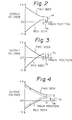
- the output voltage of a servo amplifier circuit having a construction shown in Fig. 1, has characteristics as shown in Fig. 2 or Fig. 3.
- a curve which is denoted by "FWD seek” shows an output voltage of the servo amplifier circuit of Fig. 1 in the forward seek mode
- a curve which is denoted by “REV seek” shows an output voltage of the servo amplifier circuit of Fig. 1 in the reverse seek mode, as a function of the position of the magnetic head
- the position "O” denotes a target track position of the magnetic head.
- the two curves corresponding to the forward seek and the reverse seek are apart from each other as shown in Fig. 2, and when the offset generated in the amplifier portion has the opposite polarity to the polarity of the remaining component (other than the offset) of a non-zero output of the amplifier portion, i.e., positive, the two curves corresponding to the forward seek and the reverse seek intersect as shown in Fig. 3.
- the control is changed from the velocity servo control as mentioned above to a fine position control when the magnetic head approaches the target track position to a predetermined degree. Therefore, the above non-zero values V F and V R in the vicinity of the target track position in the velocity servo affect a positioning accuracy of the magnetic head. In particular, the difference between the values V F and V R results in different positioning accuracy in the forward seek mode and the reverse seek mode.
- the manual offset adjust circuit 29 is provided.
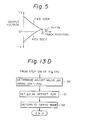
- the operator can manually adjust the output level of the above-mentioned amplifier portion at the manual offset adjust circuit 29, and the output voltages of the servo amplifier circuit in the forward seek mode and the reverse seek mode are changed as shown in Fig. 4, and thus the characteristics of the output voltage of the servo amplifier circuit as shown in Fig. 5 can be obtained.
- the object of the present invention is to provide a servo amplifier circuit having an amplifier portion and a inverting portion which inverts a polarity of an output of the amplifier, whereby a difference between the offsets which appear in the output voltages when the inverting portion operates and when the inverting portion does not operate, can be automatically reduced.
- a servo amplifier circuit as defined in claim 1.
- Figure 6 shows the basic construction of the present invention.
- Fig. 6 1 denotes a forward offset obtaining means
- 2 denotes a reverse offset obtaining means
- 3 denotes a target value obtaining means
- 4 denotes an offset adjusting value obtaining means
- 5 denotes an absolute value outputting means
- 6 denotes a control direction outputting means
- 7 denotes an output voltage detecting means
- 8 denotes an offset adjusting means
- 9 denotes an amplifier means
- 10 denotes a forward/reverse conversion means.
- the output voltage detecting means 7 detects an output voltage of the servo amplifier circuit.
- the target value obtaining means 3 obtains a target value of the output voltage.
- the absolute value outputting means 5 outputs an absolute value of the target value.
- the control direction outputting means 6 outputs a sign of the target value.
- the amplifier means 9 amplifies an output of the absolute value outputting means 5.
- the forward/reverse conversion means 10 passes the output of the amplifier means 9 with or without inversion in accordance with the sign of the target value.
- the forward offset obtaining means 1 obtains an output voltage of the servo amplifier circuit without an adjustment when the absolute value is set to zero and the sign is set to plus, as a forward offset.
- the reverse offset obtaining means 2 obtains an output voltage of the offset adjust circuit without an adjustment when the absolute value is set to zero and the sign is set to minus, as a reverse offset.
- the offset adjusting value obtaining means 4 obtains an offset adjusting value using the forward offset and the reverse offset.
- the offset adjusting means 8 modifies the input of the amplifier means 9 using the offset adjusting value, so that the difference between the forward offset and the reverse offset is reduced.
- the target value obtaining means 3, the absolute value outputting means 5, the control direction outputting means 6, the amplifier means 9, and the forward/reverse conversion means 10 substantially correspond to the conventional construction shown in Fig. 1.
- an automatic adjustment of the offset in the output of the servo amplifier circuit is carried out through the following steps.
- an output voltage of the offset adjust circuit without an adjustment when the absolute value is set to zero and the sign is set to plus, is obtained, as a forward offset.
- an offset adjusting value is obtained by using the forward offset and the reverse offset.
- the input of the amplifier means 9 is modified using the offset adjusting value.
- the above modification of the input of the amplifier means 9 using the offset adjusting value is achieved by adding, i.e., the summation of the output of the absolute value outputting means 5 and the offset adjusting value is applied instead of the output of the absolute value outputting means 5 only.
- the above offset adjusting value is obtained as half of the deviation of the reverse offset from the forward offset.
- Figure 7 shows a hardware construction realizing the embodiment of the present invention.
- Fig. 7 11 denotes a CPU, 12 and 13 each denote a register, 20 denotes a target velocity voltage output circuit, 21 denotes an offset adjusting value digital to analog converter, 22 denotes a target velocity voltage digital to analog converter, 23 denotes a gain characteristic setting circuit, 24 denotes an operational amplifier, 30 denotes a forward/reverse conversion circuit, 31 denotes an inverting amplifier, 32 and 34 each denote an ON/OFF switch, 33 denotes a logical inverter, 40 denotes a voltage detect circuit, 41 denotes a voltage analog to digital converter, 42 and 46 each denote a resistor, 43 denotes a transistor, 44 and 45 each denote a diode, and 47 denotes an operational amplifier.
- the target velocity voltage digital to analog converter 22, the gain characteristic setting circuit 23, and the operational amplifier 24 are each substantially the same as the digital to analog converter 26, the gain characteristic setting circuit 28, and the operational amplifier 27 in the construction of Fig. 1.
- the forward/reverse conversion circuit 30 is substantially the same as the corresponding one shown in Fig. 1.
- the offset adjusting value digital to analog converter 21 is provided for obtaining an analog form of an offset adjusting value, i.e., an offset adjusting voltage.
- the digital offset adjusting value is obtained in the CPU 11 by the operations described later.
- the output of the offset adjusting digital to analog converter 21 and the output of the target velocity voltage digital to analog converter 22 are each applied to the inverting input terminal of the operational amplifier 24 through a corresponding resistor.
- the terminals of the gain characteristic setting circuit 23 are each connected to the inverting input terminal and the output terminal of the operational amplifier 24, and the non-inverting input terminal of the operational amplifier 24 is connected to earth through a resistor.
- the switch 34 when the polarity of the target velocity is positive, i.e., in the forward seek mode, the switch 34 is made ON and the switch 32 is made OFF under the control of the CPU 11, and thus the output of the target velocity voltage output circuit 20 is output as the output of the servo amplifier circuit without inversion of the polarity.
- the switch 32 When the polarity of the target velocity is positive, i.e., in the forward seek mode, the switch 32 is made ON and the switch 34 is made OFF under the control of the CPU 11, and thus the polarity of the output of the target velocity voltage output circuit 20 is inverted through the inverting amplifier 31, and is output as the output of the servo amplifier circuit.
- the output of the forward/reverse conversion circuit 30 is applied to a non-inverting input terminal of the operational amplifier 47 of the voltage detect circuit 40.
- the operational amplifier 47 constitutes a voltage follower amplifier, and the output of the forward/reverse conversion circuit 30 is amplified through the voltage follower amplifier.
- the output of the voltage follower amplifier is applied to a base terminal of a pnp transistor 43 through a resistor 46.
- the base terminal of the transistor 43 is connected to a limiter circuit consisting of the diodes 44 and 45.
- the diodes 44 and 45 are connected in parallel between the base terminal of the transistor 43 and earth, where the diode 44 is connected in the direction from the base terminal of the transistor 43 to earth, and the diode 45 is connected in the direction from earth to the base terminal of the transistor 43.
- the emitter terminal of the transistor 43 is connected to a high voltage source +V o through the resistor 42, and the collector terminal of the transistor 43 is connected to earth.
- the transistor 43 and the resistor 42 constitute a level shift circuit.
- the output of the level shift circuit is obtained from the emitter terminal of the transistor 43.
- the level shift circuit is provided because the range of the input voltage of commercially available analog to digital converters must be in a voltage region of a single polarity.
- the effect of the above level shift circuit is shown in Figure 9.
- the output of the level shift circuit is input into the voltage analog to digital converter 41, and then the digital output of the voltage analog to digital converter 41 is input into the CPU 11.
- Figures 10 and 11 each show a input-output relationship in the offset adjusting value digital to analog converter 21 and the voltage analog to digital converter 41.
- the resolution of the voltage analog to digital converter 41 shown in Fig. 11 is much lower than the resolution of the offset adjust value digital to analog converter 21 shown in Fig. 10.
- the lower resolution of the detected voltage analog to digital converter 41 is allowed by carrying out operations for obtaining an offset adjusting value according to the embodiment of the present invention, which is described later.
- the output of the servo amplifier circuit shown in Fig. 7 is input into the velocity control circuit as the conventional servo amplifier circuit shown in Fig. 1, to obtain the motor driving current.
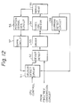
- Figure 12 shows a construction of a motor driving system including the velocity control circuit.
- reference numeral 51 denotes a velocity detect circuit
- 52 denotes a deviation detect circuit
- 53 denotes a driver circuit
- 54 denotes a voice coil motor
- 55 denotes a servo head
- 56 denotes a position signal generation circuit
- 57 denotes a differential circuit
- 58 denotes a current detect circuit.
- the servo head 55 is a magnetic head the track position of which is controlled to be changed by using the velocity control system including the servo amplifier circuit according to the present invention.
- the voice coil motor 54 is used for moving the servo head in accordance with the motor driving current which is supplied from the driver circuit 53.
- the position signal generation circuit 56 detects a track position of the servo head 55 by counting the number of the tracks, and outputting a position signal.
- the position signal is differentiated by the differential circuit 57 to obtain velocity information, and then, the result is input into the velocity detect circuit 51.
- the motor driving current is detected by the current detect circuit 58, and the detected current is also input into the velocity detect circuit 51.
- the velocity detect circuit 51 detects the velocity of the servo head 55 using both the information obtained through the position signal and the driving current.
- the output of the velocity detect circuit 51 is input into one of the input terminals of the deviation detect circuit 52, as a detected velocity.
- the output of the servo amplifier circuit according to the present invention i.e., the output of the forward/reverse conversion circuit 30 is input into the other input terminal of the deviation detect circuit 52, as a target velocity (voltage).
- the deviation detect circuit 52 obtains a deviation of the detected velocity from the target velocity, and the result is input into the driver circuit 53.
- the driver circuit 53 outputs the motor driving current according to the output of the deviation detect circuit 52.
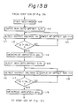
- Figures 13A, 13B, and 13C show a flow of operations for obtaining an amount of the offset adjusting value.
- the servo system for the magnetic head in the magnetic disk device including the servo amplifier circuit according to the present invention is set to an automatic adjusting mode, i.e., the servo system is initialized by the operations including the following first to third operations.
- the servo loop in the servo system is made OFF.
- the servo loop is a negative feedback loop shown in Fig. 12.
- Fig. 12 the operation of the construction of Fig. 12 is made OFF under the control of the CPU 11.
- digital data corresponding to the zero output voltage of the target velocity voltage digital to analog converter 22 is set as an input of the target velocity voltage digital to analog converter 22, and thus the output voltage of the target velocity voltage digital to analog converter 22 is made zero.
- the digital value "80H” (where H indicates that "80” is a number expressed in a hexadecimal notation) is input into the offset adjusting value digital to analog converter 21.
- "80H” is the center value of the input range of an eight-bit digital to analog converter, and this value corresponds to the zero level output of the offset adjusting value digital to analog converter 21, i.e., corresponds to the zero level of the offset adjust voltage.
- the forward seek mode is set, i.e., the switch 34 is set ON and the switch 32 is set OFF in the forward/reverse conversion circuit 30.
- step 103 the output voltage of the servo amplifier circuit of Fig. 7 is detected as a forward offset "FWD" in the condition which was set in the steps 101 and 102.
- the operations in the steps 102 and 103 corresponds to the function of the forward offset obtaining means 1.
- the reverse seek mode is set, i.e., the switch 32 is set ON and the switch 34 is set OFF in the forward/reverse conversion circuit 30.
- step 105 the output voltage of the servo amplifier circuit of Fig. 7 is detected as a reverse offset "REV" in the condition which was set in the steps 101 and 104.
- the forward offset "FWD” and the reverse offset “REV” are compared and it is determined which is larger than the other.
- the forward offset "FWD” is larger than the reverse offset "REV"
- the forward offset “FWD” is held in the register 12 as a value "VAL1” and the reverse offset “REV” is held in the register 13 as a value "VAL2" in the step 107
- the reverse offset "REV” is held in the register 12 as a value "VAL1” and the forward offset "FWD” is held in the register 13 as a value "VAL2” in the step 108.
- the forward seek mode is set, and then the aforementioned digital data "80H" is input into the offset adjusting digital to analog converter 21, in the step 110.
- the output voltage V f is detected by the voltage detect circuit 40, and then the detected value V f is compared with the above value "VAL1" which has been held in the register 12, in the step 112.
- the variation of the input of the offset adjusting value digital to analog converter 21 when the detected value V f becomes larger than the value "VAL1" is memorized as " ⁇ H 1 " in the step 114.
- the variation of the input of the offset adjusting value digital to analog converter 21 is incremented in the step 113, and then the output voltage V f is detected again in the step 111.
- step 115 the aforementioned digital data "80H" is input into the offset adjusting digital to analog converter 21.
- the output voltage V f is detected by the voltage detect circuit 40, and then the detected value V f is compared with the above value "VAL2" which has been held in the register 13, in the step 117.
- the variation of the input of the offset adjusting value digital to analog converter 21 when the detected value V f becomes smaller than the value "VAL2" is memorized as " ⁇ H 2 " in the step 119.
- the variation of the input of the offset adjusting value digital to analog converter 21 is decremented in the step 118, and then the output voltage V f is detected again in the step 116.
- the resolution of the voltage analog to digital converter 41 is lower than the resolution of the offset adjusting value digital to analog converter 21, and the gain in the amplifier portion in the target velocity voltage output circuit 20 is small in the vicinity of the target voltage value zero, generally, the output voltage V f of the servo amplifier circuit, which is obtained through the voltage analog to digital converter 41 does not respond to the small variation of the input of the offset adjusting value digital to analog converter 21, by a one to one correspondance. Therefore, the above repeating of the steps for incrementing the input of the offset adjusting value digital to analog converter 21 and comparing the resulting output voltage of the servo amplifier circuit, is necessary to obtain the information of the forward offset with a high resolution, i.e., in the resolution of the offset adjusting digital to analog converter 21.
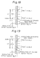
- FIG. 14 An example of the above operations in the steps 109 to 119 is shown in Figure 14.
- the scale of the input of the offset adjusting digital to analog converter 21 is shown in the up and down direction, and on the right side, the corresponding scale of the output of the voltage analog to digital converter 41 is shown.
- the above input value "80H” of the offset adjusting digital to analog converter 21 in the forward seek mode is denoted by "A”
- the above input value "80H” of the offset adjusting digital to analog converter 21 in the reverse seek mode is denoted by "B" in Fig. 14.
- step 120 of Fig. 13C the reverse seek mode is set, and then the aforementioned digital data "80H" is input into the offset adjusting digital to analog converter 21, in the step 121.
- the output voltage V r is detected by the voltage detect circuit 40, and then the detected value V r is compared with the above value "VAL1" which has been held in the register 12, in the step 123.
- the variation of the input of the offset adjusting value digital to analog converter 21 when the detected value V r becomes larger than the value "VAL1" is memorized as " ⁇ H 3 " in the step 125.
- the variation of the input of the offset adjusting value digital to analog converter 21 is decremented in the step 124, and then the output voltage V r is detected again in the step 122.
- step 126 the aforementioned digital data "80H" is input into the offset adjusting value digital to analog converter 21.
- the output voltage V r is detected by the voltage detect circuit 40, and then the detected value V r is compared with the above value "VAL2" which has been held in the register 13, in the step 128.
- the variation of the input of the offset adjusting value digital to analog converter 21 when the detected value V r becomes smaller than the value "VAL2" is memorized as " ⁇ H 4 " in the step 130.
- the variation of the input of the offset adjusting value digital to analog converter 21 is incremented in the step 129, and then the output voltage V r is detected again in the step 127.
- FIG. 15 An example of the above operations in the steps 120 to 130 is shown in Figure 15.
- the scale of the input of the offset adjusting value digital to analog converter 21 is shown in the up and down direction, and on the right side, the corresponding scale of the output of the voltage analog to digital converter 41 is shown.
- the above input value "80H” of the offset adjusting digital to analog converter 21 in the forward seek mode is denoted by "A”
- the above input value "80H” of the offset adjusting value digital to analog converter 21 in the reverse seek mode is denoted by "B" in Fig. 15.
- the offset adjusting value is obtained using the above information on the forward and reverse offsets.
- the offset adjusting value is obtained using the above information on the forward and reverse offsets.
- the average of the above four values of the variations " ⁇ H 1 , ⁇ H 2 , ⁇ H 3 , and a ⁇ H 4 .” is obtained.
- the obtained offset adjusting value is set as the input of the offset adjusting value digital to analog converter 21, and then the automatic offset adjusting mode is ended and the system is returned to a servo mode wherein the servo loop is made ON.
- the average of the four values of the variations ⁇ H 1 , ⁇ H 2 , ⁇ H 3 , and ⁇ H 4 corresponds to half of the voltage deviation of the point A from the point B in the resolution of the offset adjusting value digital to analog converter 21.
- Figs. 18 and 19 corresponds to the characteristic curves shown in Fig. 17.
- the above operations in the offset adjusting mode can be carried out at the time of the start up of the magnetic disk device, at the time of maintainance, after a power on operation, or by a command from a host computer.
- a relatively low-resolution analog to digital converter can be used for converting a detected output voltage, further, the detected output voltage of the servo amplifier circuit is level-shifted by a level shift circuit, and therefore, the accurate detection of the output voltage near zero volt using an analog to digital converter which is commercially available at a low cost, can be carried out.
Description
- The present invention relates to a servo amplifier circuit. In particular, it relates to a servo amplifier circuit having an amplifier portion and an inverting portion which inverts a polarity of an output of the amplifier.
- The present invention is applicable to a servo system for a magnetic head in a magnetic disk device.
- In a magnetic disk device, the magnetic head is moved in two seek modes, a forward seek mode and a reverse seek mode, each corresponding to the direction of the motion of the magnetic head, i.e., corresponding to which side of the target track position the magnetic head exists when the target track position is commanded.
- In a servo system for a magnetic head in a magnetic disk device, a servo amplifier circuit having an amplifier portion and an inverting portion which inverts the polarity of the output of the amplifier, is used since a specific non-linear amplifier gain characteristics are used because a fast seeking speed is required when the magnetic head is far from the target track position and a slow seeking speed is required when the magnetic head is near the target track position, and the characteristics are the same in both the forward seek mode and the reverse seek mode without the polarity. The inverting portion operates when the magnetic disk device is in a reverse seek mode.
- Figure 1 shows a construction of the conventional servo amplifier circuit used for a velocity control system for a magnetic head in a magnetic disk device.
- In Fig. 1,
reference numeral 14 denotes a CPU, 25 denotes a target velocity setting circuit, 26 denotes a digital to analog converter, 27 denotes an operational amplifier, 28 denotes a gain characteristics setting circuit, 29 denotes a manual offset adusting circuit, 30 denotes a forward/reverse conversion circuit, and 50 denotes a velocity control circuit. - The
CPU 14 calculates and commands a target value of the velocity of the magnetic head as a digital form of a voltage value, based on the difference between the target track position and the actual track position at that time. The digital toanalog converter 26 converts the digital target velocity voltage to an analog form. The analog target velocity voltage is input to an amplifier portion consisting of an operational amplifier, a gain characteristics setting circuit 28, a manualoffset adusting circuit 29, and resistors. - The gain characteristics setting circuit 28 is a resistor having a value which varies with a voltage applied between both terminals of the gain characteristics setting circuit 28, and the varying characteristics are such that the gain of the amplifier portion is large when the magnetic head is far from the target track position and the gain is small when the magnetic head is near the target track position. These characteristics are required because a fast seeking speed is required when the magnetic head is far from the target track position and because a slow seeking speed is required when the magnetic head is near from the target track position.
- The manual
offset adusting circuit 29 is provided for manually adjusting an offset of the amplifier portion. - The forward/
reverse conversion circuit 30 realizes the above inverting portion, and operates in the reverse seek mode under the control of theCPU 14. The output of the above amplifier portion passes through the forward/reverse conversion circuit 30 without polarity invertion in the forward seek mode, and the output of the above amplifier portion is inverted at the forward/reverse conversion circuit 30 in a reverse seek mode. The output of the forward/reverse conversion circuit 30 is input to thevelocity control circuit 50 as a target voltage. - The
velocity control circuit 50 detects the actual velocity of the magnetic head as a voltage, obtains a deviation of the actual velocity voltage from the target voltage, and then controls an current for driving a motor. - It is well-known that an analog circuit has an offset in its output, for example, an amplifier circuit comprising an operational amplifier has an offset in its output voltage, i.e., it has a non-zero voltage output (offset) even when its input voltage is zero.
- Due to an offset generated in the amplifier portion comprising the
operational amplifier 27, the gain characteristics setting portion 28, the manualoffset adjusting portion 29, and the resistors, and another offset generated in the invertingportion 30, the output voltage of a servo amplifier circuit having a construction shown in Fig. 1, has characteristics as shown in Fig. 2 or Fig. 3. - In Figs. 2 and 3, a curve which is denoted by "FWD seek" shows an output voltage of the servo amplifier circuit of Fig. 1 in the forward seek mode, and a curve which is denoted by "REV seek" shows an output voltage of the servo amplifier circuit of Fig. 1 in the reverse seek mode, as a function of the position of the magnetic head, and the position "O" denotes a target track position of the magnetic head.
- In Figs. 2 and 3, the overall position of the two curves are shifted with reference to the zero volt line due to the offset generated in the following stage of the amplifier portion in the construction of Fig. 1.
- When the offset generated in the amplifier portion has the same polarity as the polarity of the remaining component (other than the offset) of a non-zero output of the amplifier portion, i.e., positive, the two curves corresponding to the forward seek and the reverse seek are apart from each other as shown in Fig. 2, and when the offset generated in the amplifier portion has the opposite polarity to the polarity of the remaining component (other than the offset) of a non-zero output of the amplifier portion, i.e., positive, the two curves corresponding to the forward seek and the reverse seek intersect as shown in Fig. 3.
- Further, in Figs. 2 and 3, the above curves of the FWD seek and the REV seek continue to the target track position, and each voltage in the forward seek mode and the reverse seek mode has a non-zero value, respectively denoted by VF and VR.
- Generally, in a servo system of a magnetic head which is used in a magnetic disk device, the control is changed from the velocity servo control as mentioned above to a fine position control when the magnetic head approaches the target track position to a predetermined degree. Therefore, the above non-zero values VF and VR in the vicinity of the target track position in the velocity servo affect a positioning accuracy of the magnetic head. In particular, the difference between the values VF and VR results in different positioning accuracy in the forward seek mode and the reverse seek mode.
- Therefore, it is necessary to reduce the above difference between the output voltage values VF and VR in the vicinity of the target track position, i.e., at the target track position in the velocity servo stage.
- For the above purpose, the manual offset adjust
circuit 29 is provided. The operator can manually adjust the output level of the above-mentioned amplifier portion at the manual offset adjustcircuit 29, and the output voltages of the servo amplifier circuit in the forward seek mode and the reverse seek mode are changed as shown in Fig. 4, and thus the characteristics of the output voltage of the servo amplifier circuit as shown in Fig. 5 can be obtained. - However, the manual adjusting of offset is troublesome, and the manual adjusting of offset cannot follow the changes of the characteristics of the analog circuit due to a deterioration due to age or temperature variation.
- Otherwise, it may be possible to reduce the offset by using high-precision components for constructing the circuit. However, this causes an increase in cost.
- For an example of an offset adjustment circuit corresponding to the preamble of
claim 1, reference can be made to DE-A-26 29 473. - There is also known from US-A-4 775 825 a head positioning system that seeks to overcome the positioning error due to hysteresis in the stepper motor. To this end, the oscillation damping condition is controlled when the stepper motor enters a damped oscillation phase in the vicinity of the target position. The damping condition is controlled by varying the solid friction factor of the mechanism or the drawback torque constant of the stepper motor.
- The object of the present invention is to provide a servo amplifier circuit having an amplifier portion and a inverting portion which inverts a polarity of an output of the amplifier, whereby a difference between the offsets which appear in the output voltages when the inverting portion operates and when the inverting portion does not operate, can be automatically reduced.
- According to the present invention, there is provided a servo amplifier circuit as defined in
claim 1. - In the drawings:
- Figure 1 shows the construction of a conventional servo amplifier circuit;
- Figures 2 and 3 show an example of output voltages of the conventional servo amplifier circuit shown in Fig. 1;
- Figure 4 shows an example of a conventional manual offset adjusting procedure;
- Figure 5 shows an example of the output voltages after offset adjustment;
- Figure 6 shows the basic construction of the present invention;
- Figure 7 shows the construction of an embodiment of the present invention;
- Figure 8 shows the input-output relationship in the limiter circuit in the
voltage detection circuit 40 in Fig. 7; - Figure 9 shows the input-output relationship in the level shift circuit in the voltage detect
circuit 40 in Fig. 7; - Figure 10 shows the input-output relationship in the digital to
analog converter 21 in Fig. 7; - Figure 11 shows the input-output relationship in the analog to
digital converter 41 in Fig. 7; - Figure 12 shows the construction of the
velocity control circuit 50 in an embodiment of the present invention; - Figures 13A to 13D show a flow of the operations for obtaining an amount of the offset adjust value; and
- Figures 14 to 19 show the operations for obtaining an amount of the offset adjust value.
- Before describing the preferred embodiment of the the present invention, first, the basic principle of the present invention is explained below.
- Figure 6 shows the basic construction of the present invention.
- In Fig. 6, 1 denotes a forward offset obtaining means, 2 denotes a reverse offset obtaining means, 3 denotes a target value obtaining means, 4 denotes an offset adjusting value obtaining means, 5 denotes an absolute value outputting means, 6 denotes a control direction outputting means, 7 denotes an output voltage detecting means, 8 denotes an offset adjusting means, 9 denotes an amplifier means, and 10 denotes a forward/reverse conversion means.
- The output voltage detecting means 7 detects an output voltage of the servo amplifier circuit.
- The target value obtaining means 3 obtains a target value of the output voltage.
- The absolute value outputting means 5 outputs an absolute value of the target value.
- The control direction outputting means 6 outputs a sign of the target value.
- The amplifier means 9 amplifies an output of the absolute value outputting means 5.
- The forward/reverse conversion means 10 passes the output of the amplifier means 9 with or without inversion in accordance with the sign of the target value.
- The forward offset obtaining
means 1 obtains an output voltage of the servo amplifier circuit without an adjustment when the absolute value is set to zero and the sign is set to plus, as a forward offset. - The reverse offset obtaining
means 2 obtains an output voltage of the offset adjust circuit without an adjustment when the absolute value is set to zero and the sign is set to minus, as a reverse offset. - The offset adjusting
value obtaining means 4 obtains an offset adjusting value using the forward offset and the reverse offset. - The offset adjusting means 8 modifies the input of the amplifier means 9 using the offset adjusting value, so that the difference between the forward offset and the reverse offset is reduced.
- The target
value obtaining means 3, the absolute value outputting means 5, the control direction outputting means 6, the amplifier means 9, and the forward/reverse conversion means 10 substantially correspond to the conventional construction shown in Fig. 1. - According to the present invention, an automatic adjustment of the offset in the output of the servo amplifier circuit, is carried out through the following steps.
- In the first step, an output voltage of the offset adjust circuit without an adjustment when the absolute value is set to zero and the sign is set to plus, is obtained, as a forward offset.
- In the second step, an output voltage of the offset adjust circuit without an adjustment when the absolute value is set to zero and the sign is set to minus, is obtained, as a reverse offset.
- In the third step, an offset adjusting value is obtained by using the forward offset and the reverse offset.
- In the fourth step, the input of the amplifier means 9 is modified using the offset adjusting value.
- Thus, the difference between the forward offset and the reverse offset is reduced.
- In an embodiment of the present invention, the above modification of the input of the amplifier means 9 using the offset adjusting value, is achieved by adding, i.e., the summation of the output of the absolute value outputting means 5 and the offset adjusting value is applied instead of the output of the absolute value outputting means 5 only.
- Further, in an embodiment of the present invention, the above offset adjusting value is obtained as half of the deviation of the reverse offset from the forward offset.
- Next, the hardware construction of the preferred embodiment of the present invention is explained with reference to Figure 7.
- Figure 7 shows a hardware construction realizing the embodiment of the present invention.
- In Fig. 7, 11 denotes a CPU, 12 and 13 each denote a register, 20 denotes a target velocity voltage output circuit, 21 denotes an offset adjusting value digital to analog converter, 22 denotes a target velocity voltage digital to analog converter, 23 denotes a gain characteristic setting circuit, 24 denotes an operational amplifier, 30 denotes a forward/reverse conversion circuit, 31 denotes an inverting amplifier, 32 and 34 each denote an ON/OFF switch, 33 denotes a logical inverter, 40 denotes a voltage detect circuit, 41 denotes a voltage analog to digital converter, 42 and 46 each denote a resistor, 43 denotes a transistor, 44 and 45 each denote a diode, and 47 denotes an operational amplifier.
- Among the above components, the target velocity voltage digital to
analog converter 22, the gaincharacteristic setting circuit 23, and theoperational amplifier 24 are each substantially the same as the digital toanalog converter 26, the gain characteristic setting circuit 28, and theoperational amplifier 27 in the construction of Fig. 1. The forward/reverse conversion circuit 30 is substantially the same as the corresponding one shown in Fig. 1. - In the target velocity
voltage output circuit 20, the offset adjusting value digital toanalog converter 21 is provided for obtaining an analog form of an offset adjusting value, i.e., an offset adjusting voltage. The digital offset adjusting value is obtained in theCPU 11 by the operations described later. - The output of the offset adjusting digital to
analog converter 21 and the output of the target velocity voltage digital toanalog converter 22 are each applied to the inverting input terminal of theoperational amplifier 24 through a corresponding resistor. The terminals of the gaincharacteristic setting circuit 23 are each connected to the inverting input terminal and the output terminal of theoperational amplifier 24, and the non-inverting input terminal of theoperational amplifier 24 is connected to earth through a resistor. - Thus, through the above construction of the inversion amplifier, a summation of the offset adjusting value and the target velocity voltage according to the present invention is obtained.
- In the forward/
reverse conversion circuit 30, when the polarity of the target velocity is positive, i.e., in the forward seek mode, theswitch 34 is made ON and the switch 32 is made OFF under the control of theCPU 11, and thus the output of the target velocityvoltage output circuit 20 is output as the output of the servo amplifier circuit without inversion of the polarity. - When the polarity of the target velocity is positive, i.e., in the forward seek mode, the switch 32 is made ON and the
switch 34 is made OFF under the control of theCPU 11, and thus the polarity of the output of the target velocityvoltage output circuit 20 is inverted through the invertingamplifier 31, and is output as the output of the servo amplifier circuit. - The output of the forward/
reverse conversion circuit 30 is applied to a non-inverting input terminal of theoperational amplifier 47 of the voltage detectcircuit 40. Theoperational amplifier 47 constitutes a voltage follower amplifier, and the output of the forward/reverse conversion circuit 30 is amplified through the voltage follower amplifier. The output of the voltage follower amplifier is applied to a base terminal of apnp transistor 43 through aresistor 46. The base terminal of thetransistor 43 is connected to a limiter circuit consisting of thediodes - The
diodes transistor 43 and earth, where thediode 44 is connected in the direction from the base terminal of thetransistor 43 to earth, and thediode 45 is connected in the direction from earth to the base terminal of thetransistor 43. - The effect of the above limiter circuit is shown in Figure 8. Namely, the limiter circuit prevents application of an extremely high or low voltage to the next stage.
- The emitter terminal of the
transistor 43 is connected to a high voltage source +Vo through theresistor 42, and the collector terminal of thetransistor 43 is connected to earth. Thus thetransistor 43 and theresistor 42 constitute a level shift circuit. The output of the level shift circuit is obtained from the emitter terminal of thetransistor 43. - The level shift circuit is provided because the range of the input voltage of commercially available analog to digital converters must be in a voltage region of a single polarity. The effect of the above level shift circuit is shown in Figure 9.
- The output of the level shift circuit is input into the voltage analog to
digital converter 41, and then the digital output of the voltage analog todigital converter 41 is input into theCPU 11. - Figures 10 and 11 each show a input-output relationship in the offset adjusting value digital to
analog converter 21 and the voltage analog todigital converter 41. - As shown in Figs. 10 and 11, the resolution of the voltage analog to
digital converter 41 shown in Fig. 11 is much lower than the resolution of the offset adjust value digital toanalog converter 21 shown in Fig. 10. - The lower resolution of the detected voltage analog to
digital converter 41 is allowed by carrying out operations for obtaining an offset adjusting value according to the embodiment of the present invention, which is described later. - The output of the servo amplifier circuit shown in Fig. 7 is input into the velocity control circuit as the conventional servo amplifier circuit shown in Fig. 1, to obtain the motor driving current.
- Figure 12 shows a construction of a motor driving system including the velocity control circuit.
- In Fig. 12,
reference numeral 51 denotes a velocity detect circuit, 52 denotes a deviation detect circuit, 53 denotes a driver circuit, 54 denotes a voice coil motor, 55 denotes a servo head, 56 denotes a position signal generation circuit, 57 denotes a differential circuit, and 58 denotes a current detect circuit. - The
servo head 55 is a magnetic head the track position of which is controlled to be changed by using the velocity control system including the servo amplifier circuit according to the present invention. - The
voice coil motor 54 is used for moving the servo head in accordance with the motor driving current which is supplied from thedriver circuit 53. - The position
signal generation circuit 56 detects a track position of theservo head 55 by counting the number of the tracks, and outputting a position signal. The position signal is differentiated by thedifferential circuit 57 to obtain velocity information, and then, the result is input into the velocity detectcircuit 51. - On the other hand, the motor driving current is detected by the current detect
circuit 58, and the detected current is also input into the velocity detectcircuit 51. - The velocity detect
circuit 51 detects the velocity of theservo head 55 using both the information obtained through the position signal and the driving current. - The output of the velocity detect
circuit 51 is input into one of the input terminals of the deviation detectcircuit 52, as a detected velocity. The output of the servo amplifier circuit according to the present invention, i.e., the output of the forward/reverse conversion circuit 30 is input into the other input terminal of the deviation detectcircuit 52, as a target velocity (voltage). - The deviation detect
circuit 52 obtains a deviation of the detected velocity from the target velocity, and the result is input into thedriver circuit 53. Thedriver circuit 53 outputs the motor driving current according to the output of the deviation detectcircuit 52. - Figures 13A, 13B, and 13C show a flow of operations for obtaining an amount of the offset adjusting value.
- In the
step 101 of Fig. 13A, the servo system for the magnetic head in the magnetic disk device including the servo amplifier circuit according to the present invention, is set to an automatic adjusting mode, i.e., the servo system is initialized by the operations including the following first to third operations. - In the first operation of the initialization, the servo loop in the servo system is made OFF. The servo loop is a negative feedback loop shown in Fig. 12. Thus the operation of the construction of Fig. 12 is made OFF under the control of the
CPU 11. - In the second operation of the initialization, digital data corresponding to the zero output voltage of the target velocity voltage digital to
analog converter 22, is set as an input of the target velocity voltage digital toanalog converter 22, and thus the output voltage of the target velocity voltage digital toanalog converter 22 is made zero. - In the third operation of the initialization, the digital value "80H" (where H indicates that "80" is a number expressed in a hexadecimal notation) is input into the offset adjusting value digital to
analog converter 21. "80H" is the center value of the input range of an eight-bit digital to analog converter, and this value corresponds to the zero level output of the offset adjusting value digital toanalog converter 21, i.e., corresponds to the zero level of the offset adjust voltage. - In the
step 102, the forward seek mode is set, i.e., theswitch 34 is set ON and the switch 32 is set OFF in the forward/reverse conversion circuit 30. - In the
step 103, the output voltage of the servo amplifier circuit of Fig. 7 is detected as a forward offset "FWD" in the condition which was set in thesteps - The operations in the
steps means 1. - In the
step 104, the reverse seek mode is set, i.e., the switch 32 is set ON and theswitch 34 is set OFF in the forward/reverse conversion circuit 30. - In the
step 105, the output voltage of the servo amplifier circuit of Fig. 7 is detected as a reverse offset "REV" in the condition which was set in thesteps - The operations in the
steps means 2. - In the
step 106, the forward offset "FWD" and the reverse offset "REV" are compared and it is determined which is larger than the other. - If the forward offset "FWD" is larger than the reverse offset "REV", the forward offset "FWD" is held in the
register 12 as a value "VAL1" and the reverse offset "REV" is held in theregister 13 as a value "VAL2" in thestep 107, or if the reverse offset "FWD" is not larger than the forward offset "REV", the reverse offset "REV" is held in theregister 12 as a value "VAL1" and the forward offset "FWD" is held in theregister 13 as a value "VAL2" in thestep 108. - Next, in the
step 109 of Fig. 13B, the forward seek mode is set, and then the aforementioned digital data "80H" is input into the offset adjusting digital toanalog converter 21, in thestep 110. - In the
step 111, the output voltage Vf is detected by the voltage detectcircuit 40, and then the detected value Vf is compared with the above value "VAL1" which has been held in theregister 12, in thestep 112. - If it is determined that the detected value Vf is larger than the value "VAL1" in the
step 112, the variation of the input of the offset adjusting value digital toanalog converter 21 when the detected value Vf becomes larger than the value "VAL1", is memorized as "ΔH1" in thestep 114. - If it is determined that the detected value Vf is not larger than the value "VAL1" in the
step 112, the variation of the input of the offset adjusting value digital toanalog converter 21 is incremented in thestep 113, and then the output voltage Vf is detected again in thestep 111. - Namely, in the
steps 110 to 114, the variation of the input value of the offset adjusting value digital toanalog converter 21 in the increasing direction when the corresponding voltage output Vf becomes larger than the value "VAL1", is obtained and is memorized as "ΔH1". - Then, in the
step 115, the aforementioned digital data "80H" is input into the offset adjusting digital toanalog converter 21. - In the
step 116, the output voltage Vf is detected by the voltage detectcircuit 40, and then the detected value Vf is compared with the above value "VAL2" which has been held in theregister 13, in thestep 117. - If it is determined that the detected value Vf is smaller than the value "VAL2" in the
step 117, the variation of the input of the offset adjusting value digital toanalog converter 21 when the detected value Vf becomes smaller than the value "VAL2", is memorized as " ΔH2" in thestep 119. - If it is determined that the detected value Vf is not smaller than the value "VAL2" in the
step 117, the variation of the input of the offset adjusting value digital toanalog converter 21 is decremented in thestep 118, and then the output voltage Vf is detected again in thestep 116. - Namely, in the
steps 115 to 119, the variation of the input value of the offset adjusting digital toanalog converter 21 in the decreasing direction when the corresponding voltage output V, becomes smaller than the value "VAL2", is obtained and is memorized as "ΔH2". - Since the resolution of the voltage analog to
digital converter 41 is lower than the resolution of the offset adjusting value digital toanalog converter 21, and the gain in the amplifier portion in the target velocityvoltage output circuit 20 is small in the vicinity of the target voltage value zero, generally, the output voltage Vf of the servo amplifier circuit, which is obtained through the voltage analog todigital converter 41 does not respond to the small variation of the input of the offset adjusting value digital toanalog converter 21, by a one to one correspondance. Therefore, the above repeating of the steps for incrementing the input of the offset adjusting value digital toanalog converter 21 and comparing the resulting output voltage of the servo amplifier circuit, is necessary to obtain the information of the forward offset with a high resolution, i.e., in the resolution of the offset adjusting digital toanalog converter 21. - In other words, a high resolution is not required for the voltage analog to
digital converter 41 when carrying out the above operations. - An example of the above operations in the
steps 109 to 119 is shown in Figure 14. On the left side of Fig. 14, the scale of the input of the offset adjusting digital toanalog converter 21 is shown in the up and down direction, and on the right side, the corresponding scale of the output of the voltage analog todigital converter 41 is shown. The above input value "80H" of the offset adjusting digital toanalog converter 21 in the forward seek mode is denoted by "A", and the above input value "80H" of the offset adjusting digital toanalog converter 21 in the reverse seek mode is denoted by "B" in Fig. 14. - Next, in the
steps 120 to 130 of Fig. 13C, the operations similar to the operations in theabove steps 109 to 119 are carried out in the reverse seek mode. - In the
step 120 of Fig. 13C, the reverse seek mode is set, and then the aforementioned digital data "80H" is input into the offset adjusting digital toanalog converter 21, in thestep 121. - In the
step 122, the output voltage Vr is detected by the voltage detectcircuit 40, and then the detected value Vr is compared with the above value "VAL1" which has been held in theregister 12, in thestep 123. - If it is determined that the detected value Vr is larger than the value "VAL1" in the
step 123, the variation of the input of the offset adjusting value digital toanalog converter 21 when the detected value Vr becomes larger than the value "VAL1", is memorized as "ΔH3" in thestep 125. - If it is determined that the detected value Vr is not larger than the value "VAL1" in the
step 123, the variation of the input of the offset adjusting value digital toanalog converter 21 is decremented in thestep 124, and then the output voltage Vr is detected again in thestep 122. - Namely, in the
steps 121 to 125, the variation of the input value of the offset adjusting value digital toanalog converter 21 in the decreasing direction when the corresponding voltage output Vr becomes larger than the value "VAL1", is obtained and is memorized as "Δ H3". - Then, in the
step 126, the aforementioned digital data "80H" is input into the offset adjusting value digital toanalog converter 21. - In the
step 127, the output voltage Vr is detected by the voltage detectcircuit 40, and then the detected value Vr is compared with the above value "VAL2" which has been held in theregister 13, in thestep 128. - If it is determined that the detected value Vr is smaller than the value "VAL2" in the
step 128, the variation of the input of the offset adjusting value digital toanalog converter 21 when the detected value Vr becomes smaller than the value "VAL2", is memorized as "ΔH4" in thestep 130. - If it is determined that the detected value Vr is not smaller than the value "VAL2" in the
step 128, the variation of the input of the offset adjusting value digital toanalog converter 21 is incremented in thestep 129, and then the output voltage Vr is detected again in thestep 127. - Namely, in the
steps 126 to 130, the variation of the input value of the offset adjusting digital toanalog converter 21 in the increasing direction when the corresponding voltage output Vf becomes smaller than the value "VAL2", is obtained and is memorized as "ΔH4". - An example of the above operations in the
steps 120 to 130 is shown in Figure 15. On the left side of Fig. 15, the scale of the input of the offset adjusting value digital toanalog converter 21 is shown in the up and down direction, and on the right side, the corresponding scale of the output of the voltage analog todigital converter 41 is shown. The above input value "80H" of the offset adjusting digital toanalog converter 21 in the forward seek mode is denoted by "A", and the above input value "80H" of the offset adjusting value digital toanalog converter 21 in the reverse seek mode is denoted by "B" in Fig. 15. - Finally, in the
steps 130 to 132, the offset adjusting value is obtained using the above information on the forward and reverse offsets. - In the
step 130 of Fig. 13D, the offset adjusting value is obtained using the above information on the forward and reverse offsets. In this embodiment, the average of the above four values of the variations "ΔH1, ΔH2, ΔH3, and a ΔH4." is obtained. - For example, in the example shown in Figs. 14 and 15, it is shown that ΔH1 = +2, ΔH2 = -14, ΔH3 = -14, ΔH4= +2. Therefore, the offset adjusting value is obtained as ΔH = -6.
- In the
step 131, the obtained offset adjusting value is set as the input of the offset adjusting value digital toanalog converter 21, and then the automatic offset adjusting mode is ended and the system is returned to a servo mode wherein the servo loop is made ON. - As understood by referring to Figs. 14 and 15, the average of the four values of the variations ΔH1, ΔH2, ΔH3, and ΔH4, corresponds to half of the voltage deviation of the point A from the point B in the resolution of the offset adjusting value digital to
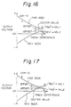
analog converter 21. - As shown in Figs. 16 and 17, the characteristic curves of the output voltages in the forward seek mode and the reverse seek mode are symmetrical with regard to the line which is defined as V= the center value of the values "FWD" and "REV", and changes symmetrically when the offset adjusting value is changed. Therefore, when the offset adjusting value is set to an amount corresponding to half of the voltage distance between the point A and the point B, the difference betweeen the output voltages in the forward seek mode and the reverse seek mode is reduced to zero. Further, if the amount is set in a high resolution as the resolution in the offset adjusting value digital to
analog converter 21 in this embodiment, the reduction of the difference is carried out at high resolution. - As the value "FWD" is larger than the value "REV" in the example shown in Figs. 14 and 15, this example corresponds to the case shown in Fig. 16. In the case shown in Fig. 16, if the offset adjusting value is set as the amount corresponding to half of the voltage deviation of the point A from the point B, i.e.,ΔH = -6, the output voltages in the forward seek mode and the reverse seek mode become equal to the center value when the track difference is zero.
- If the value "REV" is larger than the value "FWD" in the example shown in Figs. 14 and 15, the positions of the points A and B replace each other. Figures 18 and 19 shows this case, wherein ΔH1 = -2, ΔH2 = +14, ΔH3 = +14, ΔH4 = -2. Therefore, the offset adjusting value is obtained as ΔH = +6.
- The example shown in Figs. 18 and 19, corresponds to the characteristic curves shown in Fig. 17. In the case shown in Fig. 17, if the offset adjusting value is set as the amount corresponding to half of the voltage deviation of the point A from the point B, i.e., ΔH = +6, the output voltages in the forward seek mode and the reverse seek mode become equal to the center value when the track difference is zero.
- The above operations in the offset adjusting mode can be carried out at the time of the start up of the magnetic disk device, at the time of maintainance, after a power on operation, or by a command from a host computer.
- As explained above, according to the present invention, it is possible to automatically cancel the difference between the output voltages in the forward seek mode and the reverse seek mode when the actual track position is near the target track position, and thus stability and credibility of magnetic disk device is greatly improved, and a troublesome manual adjustment for cancelling the offsets, can be eliminated.
- In addition, owing to the above-mentioned operations, a relatively low-resolution analog to digital converter can be used for converting a detected output voltage, further, the detected output voltage of the servo amplifier circuit is level-shifted by a level shift circuit, and therefore, the accurate detection of the output voltage near zero volt using an analog to digital converter which is commercially available at a low cost, can be carried out.
Claims (5)
- A servo amplifier circuit, comprising:an output voltage detecting means (7) for detecting an output voltage of said servo amplifier circuit;a target value obtaining means (3) for obtaining a target value of said servo amplifier circuit;an absolute value outputting means (5) for outputting an absolute value of said target value;a control direction outputting means (6) for outputting a sign of said target value;an amplifier means (9) for amplifying an output of said absolute value outputting means;a forward/reverse conversion means (10) for passing said output of said amplifier means with or without inverting said output in accordance with said sign of said target value;characterized in that it further comprises:means (109-114) for determining the offset adjusting value that is necessary in forward seek mode for raising the output of the servo amplifier circuit above the larger one of the forward offset value and the reverse offset value;means (115-119) for determining the offset adjusting value that is necessary in forward seek mode for lowering the output of the servo amplifier circuit below the smaller one of the forward offset value and the reverse offset value;means (120-125) for determining the offset adjusting value that is necessary in reverse seek mode for raising the output of the servo amplifier circuit above the larger one of the forward offset value and the reverse offset value;means (126-130) for determining the offset adjusting value that is necessary in reverse seek mode for lowering the output of the servo amplifier circuit below the smaller one of the forward offset value and the reverse offset value; andmeans (130) for setting the adjusting value to the mean value of the adjusting values determined by said offset adjusting value determining means (109-130).
- A servo amplifier circuit according to claim 1, wherein an offset adjusting means (8) adds said offset adjusting value to said absolute value.
- A servo amplifier circuit according to claim 2, whereinsaid target value obtaining means (3), said absolute value outputting means (5), said control direction outputting means (6), a forward offset obtaining means (1), a reverse offset obtaining means (2), and said means (109-130) for determining the offset adjusting value, are realized by a microprocessor (11);said absolute value outputting means (5) further comprises a first digital to analog converter (22) for obtaining an analog value of said absolute value;an output voltage detecting means (7) comprises an analog to digital converter (41) for converting the output voltage of said forward/reverse conversion means (10) from analog to digital form before inputting the output voltage into said microprocessor (11);said offset adjusting means (8) comprising a second digital to analog converter (21) for obtaining an analog value of said offset adjusting value;the resolution of said second digital to analog converter (21) is higher than the resolution of said analog to digital converter (41), andsaid means (109-130) for determining the offset adjusting value further comprising:
a high resolution adjusting value obtaining means for obtaining a first variation of said offset adjusting value, which variation is defined as a minimum amount of variation of said offset adjusting value by which the output voltage detected by said output voltage detecting means (7) becomes higher than the higher of said forward offset and said reverse offset when said sign is set to plus; a second variation of said offset adjusting value which variation is defined as a minimum amount of variation of said offset adjusting value by which the output voltage detected by said output voltage detecting means (7) becomes lower than the lower of said forward offset and said reverse offset when said sign is set to plus; a third variation of said offset adjusting value which variation is defined as a minimum amount of variation of said offset adjusting value by which the output voltage detected by said output voltage detecting means (7) becomes higher than the higher of said forward offset and said reverse offset when said sign is set to minus; a fourth variation of said offset adjusting value which variation is defined as a minimum amount of variation of said offset adjusting value by which the output voltage detected by said output voltage detecting means (7) becomes lower than the lower of said forward offset and said reverse offset when said sign is set to minus; and a variation averaging means for obtaining an average of said first to fourth variations as said offset adjusting value. - A servo amplifier circuit according to claim 3, wherein said output voltage detecting means (7) further comprises a level shift circuit for shifting a range of a detected output voltage of said offset adjusting circuit before applying to said analog to digital converter, so that at least the lower of said forward offset and said reverse offset becomes higher than the zero level.
- A servo amplifier circuit according to claim 1, wherein said means (109-130) for determining the offset adjusting value comprises :a first offset adjusting value obtaining means (109 to 114) for obtaining a first adjusting value which is defined as a value of said offset adjusting value which makes the output voltage of said servo amplifier circuit become larger than a larger one of a first forward offset and a first reverse offset when the forward/reverse conversion means passes the output of the amplifier means without inverting the output;a second offset adjusting value obtaining means (115 to 119) for obtaining a second adjusting value, which is defined as a value of said offset adjusting value which makes the output voltage of said servo amplifier circuit become smaller than a smaller one of the first forward offset and the first reverse offset when the forward/reverse conversion means passes the output of the amplifier means without inverting the output;a third offset adjusting value obtaining means (120 to 125) for obtaining a third adjusting value, which is defined as a value of said offset adjusting value which makes the output voltage of said servo amplifier circuit become larger than a larger one of the first forward offset and the first reverse offset when the forward/reverse conversion means passes the output of the amplifier means with inverting the output;a fourth offset adjusting value obtaining means (126 to 130) for obtaining a fourth adjusting value, which is defined as a value of said offset adjusting value which makes the output voltage of said servo amplifier circuit become smaller than a smaller one of the first forward offset and the first reverse offset when the forward/reverse conversion means passes the output of the amplifier means with inverting the output; andan optimum offset adjusting value obtaining means (130) for obtaining an optimum value of said offset adjusting value, as an average of said first to fourth offset adjusting values.
Applications Claiming Priority (2)
| Application Number | Priority Date | Filing Date | Title |
|---|---|---|---|
| JP63117628A JPH0757111B2 (en) | 1988-05-13 | 1988-05-13 | Magnetic disk servo circuit |
| JP117628/88 | 1988-05-13 |
Publications (3)
| Publication Number | Publication Date |
|---|---|
| EP0342130A2 EP0342130A2 (en) | 1989-11-15 |
| EP0342130A3 EP0342130A3 (en) | 1989-12-27 |
| EP0342130B1 true EP0342130B1 (en) | 1997-10-22 |
Family
ID=14716433
Family Applications (1)
| Application Number | Title | Priority Date | Filing Date |
|---|---|---|---|
| EP89401345A Expired - Lifetime EP0342130B1 (en) | 1988-05-13 | 1989-05-12 | Servo amplifier circuit |
Country Status (5)
| Country | Link |
|---|---|
| US (1) | US4908561A (en) |
| EP (1) | EP0342130B1 (en) |
| JP (1) | JPH0757111B2 (en) |
| KR (1) | KR920010004B1 (en) |
| DE (1) | DE68928394T2 (en) |
Families Citing this family (14)
| Publication number | Priority date | Publication date | Assignee | Title |
|---|---|---|---|---|
| US5063454A (en) * | 1989-01-10 | 1991-11-05 | Fujitsu Limited | Automatic adjustment method and system for servo motor circuit of a magnetic disk apparatus |
| US5231550A (en) * | 1990-03-12 | 1993-07-27 | Fujitsu Limited | Track access control system preventing unintentional delay in movement of head in non-adjusted disc device |
| US5189571A (en) * | 1990-04-30 | 1993-02-23 | Seagate Technology, Inc. | Adaptive settle time minimization for a hard disk drive |
| EP0507907B1 (en) * | 1990-09-18 | 1999-01-13 | Rodime PLC | Digital servo control system for use in disk drives |
| JPH04181551A (en) * | 1990-11-16 | 1992-06-29 | Sony Corp | Optical disk apparatus |
| US5329409A (en) * | 1991-07-24 | 1994-07-12 | Seagate Technology, Inc. | Correction of current feedback offset for disc drive servo systems |
| US5216345A (en) * | 1992-05-04 | 1993-06-01 | Hughes Aircraft Company | Mixed mode stepper motor controller and method |
| US5408367A (en) * | 1993-09-20 | 1995-04-18 | Integral Peripherals, Inc. | Method of optimizing operation of disk drive |
| US5677808A (en) * | 1994-12-19 | 1997-10-14 | Conner Peripherals, Inc. | System and method for controlling a seek operation in a disk drive |
| US5912782A (en) * | 1996-03-27 | 1999-06-15 | International Business Machines Corporation | System and method for adjusting actuator control current for directional torque variance in a disk drive |
| US5990640A (en) * | 1996-03-29 | 1999-11-23 | Aim Controls, Inc. | Motor control apparatus |
| KR20060055875A (en) * | 2004-11-19 | 2006-05-24 | 삼성전자주식회사 | Voltage detection apparatus and method in a/d converter |
| US8084969B2 (en) | 2007-10-01 | 2011-12-27 | Allegro Microsystems, Inc. | Hall-effect based linear motor controller |
| JP2010128770A (en) * | 2008-11-27 | 2010-06-10 | Toshiba Storage Device Corp | Circuit system, circuit block and electronic apparatus |
Citations (1)
| Publication number | Priority date | Publication date | Assignee | Title |
|---|---|---|---|---|
| US4775825A (en) * | 1986-06-25 | 1988-10-04 | Hitachi, Ltd. | Positioning method and apparatus therefor |
Family Cites Families (13)
| Publication number | Priority date | Publication date | Assignee | Title |
|---|---|---|---|---|
| DE2629473C2 (en) * | 1976-06-30 | 1982-10-28 | Siemens AG, 1000 Berlin und 8000 München | Circuit arrangement for moving the data heads of a disk storage device by a defined amount from the center of the data cylinder |
| US4270073A (en) * | 1979-02-28 | 1981-05-26 | Persci, Inc. | Position control in disk drive system |
| JPS57189376A (en) * | 1981-05-15 | 1982-11-20 | Toshiba Corp | Magnetic disc device |
| US4419701A (en) * | 1981-09-21 | 1983-12-06 | Quantum Corporation | Data transducer position control system for rotating disk data storage equipment |
| US4581567A (en) * | 1982-05-28 | 1986-04-08 | Citizen Watch Co., Ltd. | Device for feeding magnetic head |
| US4485418A (en) * | 1982-08-12 | 1984-11-27 | Magnetic Peripherals, Inc. | System and method of locating the center of a track on a magnetic storage disk |
| JPS59127271A (en) * | 1983-01-07 | 1984-07-23 | Canon Inc | Feeding device of transducer |
| JPS59171079A (en) * | 1983-03-18 | 1984-09-27 | Hitachi Ltd | Speed control system of magnetic disk device |
| US4630190A (en) * | 1984-02-21 | 1986-12-16 | Syquest Technology | Servo control apparatus for a disk drive |
| JPS60182072A (en) * | 1984-02-28 | 1985-09-17 | Fujitsu Ltd | Magnetic disc access system |
| JPS61229277A (en) * | 1985-04-03 | 1986-10-13 | Nec Corp | Magnetic disk device |
| US4679103A (en) * | 1986-04-29 | 1987-07-07 | International Business Machines Corporation | Digital servo control system for a data recording disk file |
| US4797756A (en) * | 1987-03-05 | 1989-01-10 | Unisys Corp. | Method for positioning head in disk drive deriving "position" offset from "quadrature" signals |
-
1988
- 1988-05-13 JP JP63117628A patent/JPH0757111B2/en not_active Expired - Fee Related
-
1989
- 1989-05-09 US US07/349,268 patent/US4908561A/en not_active Expired - Lifetime
- 1989-05-12 EP EP89401345A patent/EP0342130B1/en not_active Expired - Lifetime
- 1989-05-12 DE DE68928394T patent/DE68928394T2/en not_active Expired - Fee Related
- 1989-05-13 KR KR1019890006408A patent/KR920010004B1/en not_active IP Right Cessation
Patent Citations (1)
| Publication number | Priority date | Publication date | Assignee | Title |
|---|---|---|---|---|
| US4775825A (en) * | 1986-06-25 | 1988-10-04 | Hitachi, Ltd. | Positioning method and apparatus therefor |
Also Published As
| Publication number | Publication date |
|---|---|
| US4908561A (en) | 1990-03-13 |
| JPH01291684A (en) | 1989-11-24 |
| DE68928394T2 (en) | 1998-02-19 |
| KR920010004B1 (en) | 1992-11-10 |
| KR900019341A (en) | 1990-12-24 |
| EP0342130A3 (en) | 1989-12-27 |
| EP0342130A2 (en) | 1989-11-15 |
| JPH0757111B2 (en) | 1995-06-14 |
| DE68928394D1 (en) | 1997-11-27 |
Similar Documents
| Publication | Publication Date | Title |
|---|---|---|
| EP0342130B1 (en) | Servo amplifier circuit | |
| JP3871200B2 (en) | Magnetic disk storage device | |
| EP0381394B1 (en) | Tracking error detecting apparatus and optical disc recording and/or apparatus including the same | |
| JP2759686B2 (en) | Device for scanning record carriers | |
| US6903894B2 (en) | Magnetic disc storage apparatus | |
| US4605884A (en) | Control unit | |
| US6975479B2 (en) | Magnetic disc storage apparatus | |
| US4988933A (en) | Head driving circuit | |
| JPH05266610A (en) | Torque correcting method for actuator | |
| GB2308464A (en) | Drive system for a voice control motor | |
| US5329409A (en) | Correction of current feedback offset for disc drive servo systems | |
| WO1984004008A1 (en) | Constant bandwidth automatic gain control system | |
| US4644514A (en) | Head drive control apparatus | |
| EP0654785A1 (en) | Error correcting apparatus with error correcting signal holding function | |
| US4827464A (en) | Slider servo device | |
| KR940003549B1 (en) | Track control circuit for remote-scanning audio or viedio disk player | |
| US5347502A (en) | Focusing control system for use in an information recording and reproducing apparatus | |
| JPH0522989B2 (en) | ||
| SU1265692A1 (en) | Servo system | |
| SU1278711A1 (en) | Device for measuring parameters of linear displacement of object | |
| JP2695313B2 (en) | Actuator drive control device | |
| JPH09161423A (en) | Slider servo control method and slider servo device | |
| JPH0427725B2 (en) | ||
| KR970007802B1 (en) | Automatic focus balance control circuit | |
| JPS6259554B2 (en) |
Legal Events
| Date | Code | Title | Description |
|---|---|---|---|
| PUAI | Public reference made under article 153(3) epc to a published international application that has entered the european phase |
Free format text: ORIGINAL CODE: 0009012 |
|
| PUAL | Search report despatched |
Free format text: ORIGINAL CODE: 0009013 |
|
| AK | Designated contracting states |
Kind code of ref document: A2 Designated state(s): DE FR GB IT NL |
|
| AK | Designated contracting states |
Kind code of ref document: A3 Designated state(s): DE FR GB IT NL |
|
| 17P | Request for examination filed |
Effective date: 19900618 |
|
| 17Q | First examination report despatched |
Effective date: 19921111 |
|
| APCB | Communication from the board of appeal sent |
Free format text: ORIGINAL CODE: EPIDOS OBAPE |
|
| APCB | Communication from the board of appeal sent |
Free format text: ORIGINAL CODE: EPIDOS OBAPE |
|
| APAB | Appeal dossier modified |
Free format text: ORIGINAL CODE: EPIDOS NOAPE |
|
| GRAG | Despatch of communication of intention to grant |
Free format text: ORIGINAL CODE: EPIDOS AGRA |
|
| GRAH | Despatch of communication of intention to grant a patent |
Free format text: ORIGINAL CODE: EPIDOS IGRA |
|
| GRAH | Despatch of communication of intention to grant a patent |
Free format text: ORIGINAL CODE: EPIDOS IGRA |
|
| GRAA | (expected) grant |
Free format text: ORIGINAL CODE: 0009210 |
|
| AK | Designated contracting states |
Kind code of ref document: B1 Designated state(s): DE FR GB IT NL |
|
| PG25 | Lapsed in a contracting state [announced via postgrant information from national office to epo] |
Ref country code: IT Free format text: LAPSE BECAUSE OF FAILURE TO SUBMIT A TRANSLATION OF THE DESCRIPTION OR TO PAY THE FEE WITHIN THE PRE;WARNING: LAPSES OF ITALIAN PATENTS WITH EFFECTIVE DATE BEFORE 2007 MAY HAVE OCCURRED AT ANY TIME BEFORE 2007. THE CORRECT EFFECTIVE DATE MAY BE DIFFERENT FROM THE ONE RECORDED.SCRIBED TIME-LIMIT Effective date: 19971022 Ref country code: NL Free format text: LAPSE BECAUSE OF FAILURE TO SUBMIT A TRANSLATION OF THE DESCRIPTION OR TO PAY THE FEE WITHIN THE PRESCRIBED TIME-LIMIT Effective date: 19971022 |
|
| REF | Corresponds to: |
Ref document number: 68928394 Country of ref document: DE Date of ref document: 19971127 |
|
| ET | Fr: translation filed | ||
| NLV1 | Nl: lapsed or annulled due to failure to fulfill the requirements of art. 29p and 29m of the patents act | ||
| PLBE | No opposition filed within time limit |
Free format text: ORIGINAL CODE: 0009261 |
|
| STAA | Information on the status of an ep patent application or granted ep patent |
Free format text: STATUS: NO OPPOSITION FILED WITHIN TIME LIMIT |
|
| 26N | No opposition filed | ||
| REG | Reference to a national code |
Ref country code: GB Ref legal event code: IF02 |
|
| PGFP | Annual fee paid to national office [announced via postgrant information from national office to epo] |
Ref country code: DE Payment date: 20050506 Year of fee payment: 17 |
|
| PGFP | Annual fee paid to national office [announced via postgrant information from national office to epo] |
Ref country code: FR Payment date: 20050511 Year of fee payment: 17 Ref country code: GB Payment date: 20050511 Year of fee payment: 17 |
|
| APAH | Appeal reference modified |
Free format text: ORIGINAL CODE: EPIDOSCREFNO |
|
| PG25 | Lapsed in a contracting state [announced via postgrant information from national office to epo] |
Ref country code: GB Free format text: LAPSE BECAUSE OF NON-PAYMENT OF DUE FEES Effective date: 20060512 |
|
| PG25 | Lapsed in a contracting state [announced via postgrant information from national office to epo] |
Ref country code: DE Free format text: LAPSE BECAUSE OF NON-PAYMENT OF DUE FEES Effective date: 20061201 |
|
| GBPC | Gb: european patent ceased through non-payment of renewal fee |
Effective date: 20060512 |
|
| REG | Reference to a national code |
Ref country code: FR Ref legal event code: ST Effective date: 20070131 |
|
| PG25 | Lapsed in a contracting state [announced via postgrant information from national office to epo] |
Ref country code: FR Free format text: LAPSE BECAUSE OF NON-PAYMENT OF DUE FEES Effective date: 20060531 |