EP0339732A1 - Process for forming an integrated circuit on an N type substrate comprising PNP and NPN transistors placed vertically and insulated one from another - Google Patents
Process for forming an integrated circuit on an N type substrate comprising PNP and NPN transistors placed vertically and insulated one from another Download PDFInfo
- Publication number
- EP0339732A1 EP0339732A1 EP89201041A EP89201041A EP0339732A1 EP 0339732 A1 EP0339732 A1 EP 0339732A1 EP 89201041 A EP89201041 A EP 89201041A EP 89201041 A EP89201041 A EP 89201041A EP 0339732 A1 EP0339732 A1 EP 0339732A1
- Authority
- EP
- European Patent Office
- Prior art keywords
- region
- type
- regions
- pnp
- npn
- Prior art date
- Legal status (The legal status is an assumption and is not a legal conclusion. Google has not performed a legal analysis and makes no representation as to the accuracy of the status listed.)
- Granted
Links
- 238000000034 method Methods 0.000 title claims abstract description 19
- 239000000758 substrate Substances 0.000 title claims abstract description 9
- 238000002955 isolation Methods 0.000 claims abstract description 11
- 239000000463 material Substances 0.000 claims abstract description 4
- 239000004065 semiconductor Substances 0.000 claims abstract 2
- 238000009792 diffusion process Methods 0.000 claims description 13
- 239000002019 doping agent Substances 0.000 claims description 6
- 238000004519 manufacturing process Methods 0.000 claims 2
- 238000002513 implantation Methods 0.000 claims 1
- ZOXJGFHDIHLPTG-UHFFFAOYSA-N Boron Chemical compound [B] ZOXJGFHDIHLPTG-UHFFFAOYSA-N 0.000 description 4
- 229910052787 antimony Inorganic materials 0.000 description 4
- WATWJIUSRGPENY-UHFFFAOYSA-N antimony atom Chemical compound [Sb] WATWJIUSRGPENY-UHFFFAOYSA-N 0.000 description 4
- 229910052796 boron Inorganic materials 0.000 description 4
- 239000012535 impurity Substances 0.000 description 3
- 229910052785 arsenic Inorganic materials 0.000 description 1
- RQNWIZPPADIBDY-UHFFFAOYSA-N arsenic atom Chemical compound [As] RQNWIZPPADIBDY-UHFFFAOYSA-N 0.000 description 1
- 238000001465 metallisation Methods 0.000 description 1
- 229910021421 monocrystalline silicon Inorganic materials 0.000 description 1
Images


Classifications
-
- H—ELECTRICITY
- H01—ELECTRIC ELEMENTS
- H01L—SEMICONDUCTOR DEVICES NOT COVERED BY CLASS H10
- H01L21/00—Processes or apparatus adapted for the manufacture or treatment of semiconductor or solid state devices or of parts thereof
- H01L21/70—Manufacture or treatment of devices consisting of a plurality of solid state components formed in or on a common substrate or of parts thereof; Manufacture of integrated circuit devices or of parts thereof
- H01L21/77—Manufacture or treatment of devices consisting of a plurality of solid state components or integrated circuits formed in, or on, a common substrate
- H01L21/78—Manufacture or treatment of devices consisting of a plurality of solid state components or integrated circuits formed in, or on, a common substrate with subsequent division of the substrate into plural individual devices
- H01L21/82—Manufacture or treatment of devices consisting of a plurality of solid state components or integrated circuits formed in, or on, a common substrate with subsequent division of the substrate into plural individual devices to produce devices, e.g. integrated circuits, each consisting of a plurality of components
- H01L21/822—Manufacture or treatment of devices consisting of a plurality of solid state components or integrated circuits formed in, or on, a common substrate with subsequent division of the substrate into plural individual devices to produce devices, e.g. integrated circuits, each consisting of a plurality of components the substrate being a semiconductor, using silicon technology
- H01L21/8222—Bipolar technology
- H01L21/8228—Complementary devices, e.g. complementary transistors
- H01L21/82285—Complementary vertical transistors
-
- H—ELECTRICITY
- H01—ELECTRIC ELEMENTS
- H01L—SEMICONDUCTOR DEVICES NOT COVERED BY CLASS H10
- H01L21/00—Processes or apparatus adapted for the manufacture or treatment of semiconductor or solid state devices or of parts thereof
- H01L21/70—Manufacture or treatment of devices consisting of a plurality of solid state components formed in or on a common substrate or of parts thereof; Manufacture of integrated circuit devices or of parts thereof
- H01L21/71—Manufacture of specific parts of devices defined in group H01L21/70
- H01L21/76—Making of isolation regions between components
- H01L21/761—PN junctions
-
- H—ELECTRICITY
- H01—ELECTRIC ELEMENTS
- H01L—SEMICONDUCTOR DEVICES NOT COVERED BY CLASS H10
- H01L27/00—Devices consisting of a plurality of semiconductor or other solid-state components formed in or on a common substrate
- H01L27/02—Devices consisting of a plurality of semiconductor or other solid-state components formed in or on a common substrate including semiconductor components specially adapted for rectifying, oscillating, amplifying or switching and having potential barriers; including integrated passive circuit elements having potential barriers
- H01L27/04—Devices consisting of a plurality of semiconductor or other solid-state components formed in or on a common substrate including semiconductor components specially adapted for rectifying, oscillating, amplifying or switching and having potential barriers; including integrated passive circuit elements having potential barriers the substrate being a semiconductor body
- H01L27/08—Devices consisting of a plurality of semiconductor or other solid-state components formed in or on a common substrate including semiconductor components specially adapted for rectifying, oscillating, amplifying or switching and having potential barriers; including integrated passive circuit elements having potential barriers the substrate being a semiconductor body including only semiconductor components of a single kind
- H01L27/082—Devices consisting of a plurality of semiconductor or other solid-state components formed in or on a common substrate including semiconductor components specially adapted for rectifying, oscillating, amplifying or switching and having potential barriers; including integrated passive circuit elements having potential barriers the substrate being a semiconductor body including only semiconductor components of a single kind including bipolar components only
- H01L27/0823—Devices consisting of a plurality of semiconductor or other solid-state components formed in or on a common substrate including semiconductor components specially adapted for rectifying, oscillating, amplifying or switching and having potential barriers; including integrated passive circuit elements having potential barriers the substrate being a semiconductor body including only semiconductor components of a single kind including bipolar components only including vertical bipolar transistors only
- H01L27/0826—Combination of vertical complementary transistors
Definitions
- the present invention concerns a process for forming an integrated circuit on an N type substrate, comprising PNP and NPN transistors with vertical current flow, insulated one from another.
- N+ type regions are diffused on a P type substrate, some of said regions being used as buried collector regions of the NPN transistors, others as buried isolation regions for the PNP transistors.
- P type regions are created by diffusion, some overlying the above-mentioned buried regions isolating the PNP transistors and destined to form the buried collector regions of said transistors, others being made directly onto the substrate and used to make isolating regions.
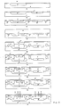
- a N type epitaxial layer is then grown, isolation regions are defined, base and emitter regions are made by diffusion, contacts are opened and the related zones metallized, all in accordance with the stages illustrated in Fig.1 .
- PNP transistors so obtained have a low level of efficiency as regards current handling (due to high base resistivity), frequency response (base being too thick) and saturation voltages (due to high collector series resistance).
- the present invention enables to overcome these draw strictlybacks since PNP and NPN transistors are thereby realized with reduced collector series resistances and practically equal low-concentration collector thicknesses, ensuring this way an excellent dynamic performance without forgoing maximum operational voltage.
- two P+ type regions 2 and 3 are made in the normal way, respectively forming the horizontal isolation region for the NPN transistor and the low-resistivity collector region for the PNP transistor.
- an N+ type region 4 is then formed serving as a low-resistivity collector region for the NPN transistor.
- An N type epitaxial layer 5 is than grown, namely one whose conductivity is of the same type as that of the substrate, as illustrated in Fig.5 .
- P+ type regions 6, 7, 8 and 9 are then diffused until they join with regions 2 and 3 ( Fig.6 ). It will be seen that regions 2, 6 and 7 taken together completely surround an N type region 10 within which the base and emitter regions of the NPN transistor will then be diffused, while regions 3, 8 and 9 all together act as a collector region for the PNP transistor.
- a P type region 12 is diffused to act as a low-concentration collector region for the PNP transistor.
- the base of said transistor is formed by known methods and is situated inside region 12: it is an N type region and is indicated by the number 13, Fig.7 .
- P+ type regions 14 and 15 are then made, respectively forming the base of the NPN transistor and the emitter of the PNP transistor, region 14 being realized in such a way to ensure a low-concentration collector thickness of transistor NPN (see thickness s1 of Fig.8) practically equal to the low-concentration collector thickness of transistor PNP (see thickness s2 of the same figure).
- regions 16, 17, 18, 19 are diffused,these being respectively the emitter of the NPN transistor and enrichments for the contact regions of the collector of the NPN transistor, of the base of the PNP transistor and of the N type isolation region formed by regions 1 and 5 together ( Fig.8 ).
- N type isolation region must be connected at the point of highest potential among all those present in the device in order to have the various components electrically insulated from each other.
- Fig.9 gives some typical profiles of doping concentration along a section of the NPN and PNP transistors made according to the invented process: the profiles represent the logarithm of concentration c (atoms/cm3) of dopant in relation to the depth p of some points on the section (the various regions touched by the section are indicated on the axis of the abscissa).
- the first of these two circumstances involves the presence of a considerable quantity of dopant in the isolation region 2 ensuring high punch-through voltages for this layer.
- the second is a necessary condition for get ting the above thicknesses equal.
- Boron the P type dopant impurity
- arsenic or antimony the N type dopant impurities which can be used to make region 4
- the surface concentration of layer 2 thus has to be lower than that of layer 4 (in the stage illustrated in Fig.5).
Landscapes
- Engineering & Computer Science (AREA)
- Power Engineering (AREA)
- Physics & Mathematics (AREA)
- Condensed Matter Physics & Semiconductors (AREA)
- General Physics & Mathematics (AREA)
- Computer Hardware Design (AREA)
- Microelectronics & Electronic Packaging (AREA)
- Manufacturing & Machinery (AREA)
- Bipolar Integrated Circuits (AREA)
- Bipolar Transistors (AREA)
Abstract
Description
- The present invention concerns a process for forming an integrated circuit on an N type substrate, comprising PNP and NPN transistors with vertical current flow, insulated one from another.
- In a well-known process for making integrated circuits of the above kind, N⁺ type regions are diffused on a P type substrate, some of said regions being used as buried collector regions of the NPN transistors, others as buried isolation regions for the PNP transistors. Than P type regions are created by diffusion, some overlying the above-mentioned buried regions isolating the PNP transistors and destined to form the buried collector regions of said transistors, others being made directly onto the substrate and used to make isolating regions.
- A N type epitaxial layer is then grown, isolation regions are defined, base and emitter regions are made by diffusion, contacts are opened and the related zones metallized, all in accordance with the stages illustrated in Fig.1.
- To overcome the punch-through problem for the PNP transistors, caused by larger concentration of impurities in the collector compared with the concentration in the base, it is advisable to increase the doping concentration of the base; for this purpose diffusion of the emitter regions of the PNP transistors is preceded by implantation of a N⁺ type region creating a structure like that illustrated in Fig.2.
- PNP transistors so obtained, however, have a low level of efficiency as regards current handling (due to high base resistivity), frequency response (base being too thick) and saturation voltages (due to high collector series resistance).
- Other processes, examples of which appear in European patent application EP 0093304 and in Tech. Dig. 1980 IEEE p.65 (see stages illustrated in Fig.3), tend to improve the process by means of triple diffused structures. Nevertheless some drawbacks are still present in these structures, such as:
- high collector series resistance for the PNP transistors;
- thickness of the collector region with low doping concentration is found to be larger in NPN transistors than in PNP transistors,
- the process is appreciably longer and more expensive. - Even other processes, examples of which appear in the GB Patent N.1,193,692 and in JP Patent N. 59-194465, tend to improve the process, but maintain some drawbacks due to the great difference of the low-concentration collector thicknesses of transistors PNP and NPN.
- The present invention enables to overcome these drawbacks since PNP and NPN transistors are thereby realized with reduced collector series resistances and practically equal low-concentration collector thicknesses, ensuring this way an excellent dynamic performance without forgoing maximum operational voltage.
- This scope is achieved through the process described by following
claim 1. - The characteristics of the process according to the invention will be made clearer by the following description and the attached drawings illustrating one non-limitative example of the same, wherein the various figures diagrammatically represent:
- Figs. 4,5,6,7,8: the structure as it appears during the different stages of the process;
- Fig.9: doping concentration profiles along a section of the NPN and PNP transistors respectively, obtained by the process as illustrated in Figs. 5 to 8.
- Referring to Fig.4, on an N type single-
crystal silicon substrate 1, two P⁺type regions region 2 an N⁺type region 4 is then formed serving as a low-resistivity collector region for the NPN transistor. - An N type
epitaxial layer 5 is than grown, namely one whose conductivity is of the same type as that of the substrate, as illustrated in Fig.5. - P⁺
type regions regions 2 and 3 (Fig.6). It will be seen thatregions N type region 10 within which the base and emitter regions of the NPN transistor will then be diffused, whileregions - Within the
N type region 11, aP type region 12 is diffused to act as a low-concentration collector region for the PNP transistor. The base of said transistor is formed by known methods and is situated inside region 12: it is an N type region and is indicated by thenumber 13, Fig.7. P⁺type regions region 14 being realized in such a way to ensure a low-concentration collector thickness of transistor NPN (see thickness s1 of Fig.8) practically equal to the low-concentration collector thickness of transistor PNP (see thickness s2 of the same figure). - Than the four
regions regions - Clearly the N type isolation region must be connected at the point of highest potential among all those present in the device in order to have the various components electrically insulated from each other.
- Finally the areas of contact are defined and the metallization process carried out thus guaranteeing interconnections among the various components of the integrated circuit.
- Fig.9 gives some typical profiles of doping concentration along a section of the NPN and PNP transistors made according to the invented process: the profiles represent the logarithm of concentration c (atoms/cm³) of dopant in relation to the depth p of some points on the section (the various regions touched by the section are indicated on the axis of the abscissa).
- How the invention achieves its purposes will now be explained.
- As stated, processes already known provide low-concentration collector thicknesses that differ considerably for the two types of transistors: thickness for the NPN transistor especially is always larger. This means that the maximum operational voltage is fixed by the PNP transistor and current handling of the NPN transistor - being inversely proportional to the square of collector thickness - is penalized as a consequence. Similarly collector series resistance is also increased.
- The process according to the invention however eliminates this difference and does so being fulfilled following conditions:
- 1) diffusion of the P⁺ type buried layer takes place before diffusion of the N⁺ type buried layer;
- 2) surface concentration of the N⁺ type buried layer is larger than that of the opposite type buried layer.
- The first of these two circumstances involves the presence of a considerable quantity of dopant in the
isolation region 2 ensuring high punch-through voltages for this layer. - The second, however, is a necessary condition for get ting the above thicknesses equal. Boron (the P type dopant impurity) is in fact known to have a higher diffusivity coefficient than either arsenic or antimony (the N type dopant impurities which can be used to make region 4); as a result equal surface concentrations generate different out-diffusions. The surface concentration of
layer 2 thus has to be lower than that of layer 4 (in the stage illustrated in Fig.5). - It could be possible to obtain this difference in surface concentration by implanting different amounts of dopant (for
instance 5·10¹³ atoms/cm² of boron and 10¹⁵ atoms/cm² of antimony) but to do so would give a P⁺ type buried layer of rather high resistivity. It is thus preferable to proceed according to the invention by implanting comparable amounts of dopant (e.g. 5·10¹⁴ atoms/cm² of boron and 10¹⁵ atoms/cm² of antimony) each followed by different diffusion cycles for the two layers (a long, high temperature diffusion for the boron, a shorter lower temperature diffusion for the antimony) so as to obtain different junction depths. - Finally it should be noted that sheet resistance values in
regions
Claims (3)
- P⁺ type regions are diffused on the N type substrate, said regions constituting the horizontal isolation region (2) of the NPN transistors and the low-resistivity collector region (3) of the PNP transistors,
-within the isolation region(2) a high-concentration N⁺ type zone (4) is diffused, said zone acting as a low-resistivity collector region for the NPN transistor,
- an N type epitaxial layer (5) is than grown all over the surface of the device,
- P⁺ type regions (6)and (7) are then diffused until they join with region (2), so as inside to define a region (10), and P⁺ type regions (8) and (9) are diffused until they join with region (3), so as inside to define a region (11), regions (6), (2) and (7) all together acting as an isolation region for the NPN transistor, regions (3), (8) and (9) all together acting as a collector region for the PNP transistor,
- within the N type region (11), a P type region (12) is diffused to act as a low-concentration collector region for the PNP transistor,
- within the P type region (12), an N type region (13) is diffused to act as the base of the PNP transistor,
- within the N type regions (10) and (13), P type regions (14) and respectively (15) are diffused to act as the base of the NPN transistor and respectively as the emitter of the PNP transistor,
- within the P type region (14), an N type region (16) is diffused to act as the emitter of the NPN transistor, said diffusions of regions (2) and (4) being made to give the region (2) a surface concentration lower than that of the region (4),
characterized in that said region 14 is realized in such a way to ensure that the low-concentration collector thickness (s1) of transistor NPN be practically equal to the low-concentration collector thickness (s2) of transistor PNP.
Applications Claiming Priority (2)
| Application Number | Priority Date | Filing Date | Title |
|---|---|---|---|
| IT20357/88A IT1218230B (en) | 1988-04-28 | 1988-04-28 | PROCEDURE FOR THE FORMATION OF AN INTEGRATED CIRCUIT ON A TYPE N SUBSTRATE, INCLUDING VERTICAL PNP AND NPN TRANSISTORS AND ISOLATED BETWEEN THEM |
| IT2035788 | 1988-04-28 |
Publications (2)
| Publication Number | Publication Date |
|---|---|
| EP0339732A1 true EP0339732A1 (en) | 1989-11-02 |
| EP0339732B1 EP0339732B1 (en) | 1993-10-27 |
Family
ID=11166004
Family Applications (1)
| Application Number | Title | Priority Date | Filing Date |
|---|---|---|---|
| EP89201041A Expired - Lifetime EP0339732B1 (en) | 1988-04-28 | 1989-04-24 | Process for forming an integrated circuit on an N type substrate comprising PNP and NPN transistors placed vertically and insulated one from another |
Country Status (5)
| Country | Link |
|---|---|
| US (1) | US4898836A (en) |
| EP (1) | EP0339732B1 (en) |
| JP (1) | JP2703798B2 (en) |
| DE (1) | DE68910169T2 (en) |
| IT (1) | IT1218230B (en) |
Cited By (8)
| Publication number | Priority date | Publication date | Assignee | Title |
|---|---|---|---|---|
| EP0439899A2 (en) * | 1990-01-25 | 1991-08-07 | Precision Monolithics Inc. | Complementary bipolar transistors compatible with CMOS process |
| EP0476757A2 (en) * | 1990-09-19 | 1992-03-25 | Koninklijke Philips Electronics N.V. | A method of manufacturing a semiconductor device |
| EP0509183A1 (en) * | 1986-10-01 | 1992-10-21 | Consorzio per la Ricerca sulla Microelettronica nel Mezzogiorno - CoRiMMe | Monolithic semiconductor device comprising an integrated control circuit and at least one power transistor integrated in the same chip and the associated manufacturing process |
| US5597742A (en) * | 1991-04-17 | 1997-01-28 | Consorzio Per La Ricerca Sulla Microelettronica Nel Mezzogiorno | Semiconductor device and method |
| EP0756329A1 (en) | 1995-07-27 | 1997-01-29 | Consorzio per la Ricerca sulla Microelettronica nel Mezzogiorno - CoRiMMe | Vertical PNP transistor and relative fabrication method |
| EP0792514A1 (en) * | 1994-11-04 | 1997-09-03 | Analog Devices, Incorporated | Integrated circuit with complementary isolated bipolar transitors and method of making same |
| EP0915508A1 (en) * | 1997-10-10 | 1999-05-12 | STMicroelectronics S.r.l. | Integrated circuit with highly efficient junction insulation |
| EP1453104A2 (en) * | 2003-02-28 | 2004-09-01 | Texas Instruments Inc. | A vertical bipolar transistor and a method of manufacture thereof |
Families Citing this family (12)
| Publication number | Priority date | Publication date | Assignee | Title |
|---|---|---|---|---|
| USRE35642E (en) * | 1987-12-22 | 1997-10-28 | Sgs-Thomson Microelectronics, S.R.L. | Integrated high-voltage bipolar power transistor and low voltage MOS power transistor structure in the emitter switching configuration and relative manufacturing process |
| IT1217323B (en) * | 1987-12-22 | 1990-03-22 | Sgs Microelettronica Spa | INTEGRATED STRUCTURE OF HIGH VOLTAGE BIPOLAR POWER TRANSISTOR AND LOW VOLTAGE POWER MOS TRANSISTOR IN THE "EMITTER SWITCHING" CONFIGURATION AND RELATED MANUFACTURING PROCESS |
| US5156989A (en) * | 1988-11-08 | 1992-10-20 | Siliconix, Incorporated | Complementary, isolated DMOS IC technology |
| US5286986A (en) * | 1989-04-13 | 1994-02-15 | Kabushiki Kaisha Toshiba | Semiconductor device having CCD and its peripheral bipolar transistors |
| JPH07105458B2 (en) * | 1989-11-21 | 1995-11-13 | 株式会社東芝 | Composite integrated circuit device |
| JP2748988B2 (en) * | 1991-03-13 | 1998-05-13 | 三菱電機株式会社 | Semiconductor device and manufacturing method thereof |
| DE69125390T2 (en) * | 1991-07-03 | 1997-08-28 | Cons Ric Microelettronica | Lateral bipolar transistor structure with integrated control circuit and integrated power transistor and their manufacturing process |
| US5702959A (en) * | 1995-05-31 | 1997-12-30 | Texas Instruments Incorporated | Method for making an isolated vertical transistor |
| JP3409548B2 (en) | 1995-12-12 | 2003-05-26 | ソニー株式会社 | Method for manufacturing semiconductor device |
| EP0809294B1 (en) * | 1996-05-21 | 2002-01-02 | Co.Ri.M.Me. Consorzio Per La Ricerca Sulla Microelettronica Nel Mezzogiorno | Power semiconductor device structure with vertical PNP transistor |
| JP3529549B2 (en) | 1996-05-23 | 2004-05-24 | 東芝マイクロエレクトロニクス株式会社 | Method for manufacturing semiconductor device |
| JPH104142A (en) * | 1996-06-18 | 1998-01-06 | Sony Corp | Manufacture of semiconductor device |
Citations (2)
| Publication number | Priority date | Publication date | Assignee | Title |
|---|---|---|---|---|
| GB1193692A (en) * | 1966-12-13 | 1970-06-03 | Texas Instruments Inc | Process for Fabricating Integrated Circuits |
| FR2095386A1 (en) * | 1970-06-20 | 1972-02-11 | Philips Nv |
Family Cites Families (11)
| Publication number | Priority date | Publication date | Assignee | Title |
|---|---|---|---|---|
| US3079287A (en) * | 1959-09-01 | 1963-02-26 | Texas Instruments Inc | Improved grown junction transistor and method of making same |
| NL145396B (en) * | 1966-10-21 | 1975-03-17 | Philips Nv | PROCESS FOR THE MANUFACTURE OF AN INTEGRATED SEMI-CONDUCTOR DEVICE AND INTEGRATED SEMIC-CONDUCTOR DEVICE, MANUFACTURED ACCORDING TO THE PROCEDURE. |
| US3930909A (en) * | 1966-10-21 | 1976-01-06 | U.S. Philips Corporation | Method of manufacturing a semiconductor device utilizing simultaneous outdiffusion during epitaxial growth |
| US4054899A (en) * | 1970-09-03 | 1977-10-18 | Texas Instruments Incorporated | Process for fabricating monolithic circuits having matched complementary transistors and product |
| US3793088A (en) * | 1972-11-15 | 1974-02-19 | Bell Telephone Labor Inc | Compatible pnp and npn devices in an integrated circuit |
| US4038680A (en) * | 1972-12-29 | 1977-07-26 | Sony Corporation | Semiconductor integrated circuit device |
| DE2351985A1 (en) * | 1973-10-17 | 1975-04-30 | Itt Ind Gmbh Deutsche | PLANAR DIFFUSION PROCESS FOR PRODUCING A MONOLITHICALLY INTEGRATED SOLID-WATER CIRCUIT |
| US3971059A (en) * | 1974-09-23 | 1976-07-20 | National Semiconductor Corporation | Complementary bipolar transistors having collector diffused isolation |
| JPS54136281A (en) * | 1978-04-14 | 1979-10-23 | Toko Inc | Semiconductor device and method of fabricating same |
| DE3361832D1 (en) * | 1982-04-19 | 1986-02-27 | Matsushita Electric Ind Co Ltd | Semiconductor ic and method of making the same |
| JPS59194465A (en) * | 1983-04-19 | 1984-11-05 | Sanken Electric Co Ltd | Manufacture of semiconductor integrated circuit |
-
1988
- 1988-04-28 IT IT20357/88A patent/IT1218230B/en active
-
1989
- 1989-04-21 US US07/341,540 patent/US4898836A/en not_active Expired - Lifetime
- 1989-04-24 EP EP89201041A patent/EP0339732B1/en not_active Expired - Lifetime
- 1989-04-24 DE DE89201041T patent/DE68910169T2/en not_active Expired - Fee Related
- 1989-04-27 JP JP1106088A patent/JP2703798B2/en not_active Expired - Fee Related
Patent Citations (2)
| Publication number | Priority date | Publication date | Assignee | Title |
|---|---|---|---|---|
| GB1193692A (en) * | 1966-12-13 | 1970-06-03 | Texas Instruments Inc | Process for Fabricating Integrated Circuits |
| FR2095386A1 (en) * | 1970-06-20 | 1972-02-11 | Philips Nv |
Non-Patent Citations (3)
| Title |
|---|
| IBM TECHNICAL DISCLOSURE BULLETIN, vol. 16, no. 6, November 1973, pages 1707-1708, New York, US; I. ANTIPOV et al.: "Fabricating complementary semiconductor devices" * |
| IBM TECHNICAL DISCLOSURE BULLETIN, vol. 17, no. 1, June 1974, pages 21-22, New York, US; J.J: CHANG et al.: "Complementary bipolar device structure" * |
| PATENT ABSTRACTS OF JAPAN, vol. 9 no. 53 (E-301)[1776], 7th March 1985; & JP-A-59 194 465 (SANKEN DENKI K.K.) 05-11-1984 * |
Cited By (13)
| Publication number | Priority date | Publication date | Assignee | Title |
|---|---|---|---|---|
| EP0509183A1 (en) * | 1986-10-01 | 1992-10-21 | Consorzio per la Ricerca sulla Microelettronica nel Mezzogiorno - CoRiMMe | Monolithic semiconductor device comprising an integrated control circuit and at least one power transistor integrated in the same chip and the associated manufacturing process |
| EP0439899A3 (en) * | 1990-01-25 | 1991-11-06 | Precision Monolithics Inc. | Complementary bipolar transistors compatible with cmos process |
| EP0439899A2 (en) * | 1990-01-25 | 1991-08-07 | Precision Monolithics Inc. | Complementary bipolar transistors compatible with CMOS process |
| EP0476757A2 (en) * | 1990-09-19 | 1992-03-25 | Koninklijke Philips Electronics N.V. | A method of manufacturing a semiconductor device |
| EP0476757A3 (en) * | 1990-09-19 | 1992-07-29 | Koninkl Philips Electronics Nv | A method of manufacturing a semiconductor device |
| US5597742A (en) * | 1991-04-17 | 1997-01-28 | Consorzio Per La Ricerca Sulla Microelettronica Nel Mezzogiorno | Semiconductor device and method |
| EP0792514A4 (en) * | 1994-11-04 | 1998-06-17 | Analog Devices Inc | Integrated circuit with complementary isolated bipolar transitors and method of making same |
| EP0792514A1 (en) * | 1994-11-04 | 1997-09-03 | Analog Devices, Incorporated | Integrated circuit with complementary isolated bipolar transitors and method of making same |
| EP0756329A1 (en) | 1995-07-27 | 1997-01-29 | Consorzio per la Ricerca sulla Microelettronica nel Mezzogiorno - CoRiMMe | Vertical PNP transistor and relative fabrication method |
| US6114746A (en) * | 1995-07-27 | 2000-09-05 | Consorzio Per La Ricerca Sullla Microelettronica Nel Mezzogiorno | Vertical PNP transistor and relative fabrication method |
| EP0915508A1 (en) * | 1997-10-10 | 1999-05-12 | STMicroelectronics S.r.l. | Integrated circuit with highly efficient junction insulation |
| EP1453104A2 (en) * | 2003-02-28 | 2004-09-01 | Texas Instruments Inc. | A vertical bipolar transistor and a method of manufacture thereof |
| EP1453104A3 (en) * | 2003-02-28 | 2005-06-01 | Texas Instruments Inc. | A vertical bipolar transistor and a method of manufacture thereof |
Also Published As
| Publication number | Publication date |
|---|---|
| EP0339732B1 (en) | 1993-10-27 |
| IT1218230B (en) | 1990-04-12 |
| JP2703798B2 (en) | 1998-01-26 |
| US4898836A (en) | 1990-02-06 |
| IT8820357A0 (en) | 1988-04-28 |
| JPH0212926A (en) | 1990-01-17 |
| DE68910169D1 (en) | 1993-12-02 |
| DE68910169T2 (en) | 1994-04-07 |
Similar Documents
| Publication | Publication Date | Title |
|---|---|---|
| EP0339732A1 (en) | Process for forming an integrated circuit on an N type substrate comprising PNP and NPN transistors placed vertically and insulated one from another | |
| US4120707A (en) | Process of fabricating junction isolated IGFET and bipolar transistor integrated circuit by diffusion | |
| US3502951A (en) | Monolithic complementary semiconductor device | |
| US4047217A (en) | High-gain, high-voltage transistor for linear integrated circuits | |
| EP0093304A1 (en) | Semiconductor IC and method of making the same | |
| US4283236A (en) | Method of fabricating lateral PNP transistors utilizing selective diffusion and counter doping | |
| US4066473A (en) | Method of fabricating high-gain transistors | |
| US4492008A (en) | Methods for making high performance lateral bipolar transistors | |
| EP0262723A2 (en) | Process for the formation of a monolithic high voltage semiconductor device | |
| US4137109A (en) | Selective diffusion and etching method for isolation of integrated logic circuit | |
| US4210925A (en) | I2 L Integrated circuit and process of fabrication | |
| US4054899A (en) | Process for fabricating monolithic circuits having matched complementary transistors and product | |
| EP0429834A1 (en) | A raised base bipolar transistor structure and its method of fabrication | |
| US4255209A (en) | Process of fabricating an improved I2 L integrated circuit utilizing diffusion and epitaxial deposition | |
| EP0051534B1 (en) | A method of fabricating a self-aligned integrated circuit structure using differential oxide growth | |
| US3770519A (en) | Isolation diffusion method for making reduced beta transistor or diodes | |
| US5837590A (en) | Isolated vertical PNP transistor without required buried layer | |
| EP0328286B1 (en) | Method of manufacturing a multicollector vertical PNP transistor | |
| US4550491A (en) | Method of making substrate injection logic operator structure | |
| US5481132A (en) | Transistor with a predetermined current gain in a bipolar integrated circuit | |
| US3968511A (en) | Semiconductor device with additional carrier injecting junction adjacent emitter region | |
| US4140559A (en) | Method of fabricating an improved substrate fed logic utilizing graded epitaxial deposition | |
| US5529939A (en) | Method of making an integrated circuit with complementary isolated bipolar transistors | |
| US3761326A (en) | Process for making an optimum high gain bandwidth phototransistor structure | |
| EP0075678B1 (en) | Semiconductor device having a schottky diode |
Legal Events
| Date | Code | Title | Description |
|---|---|---|---|
| PUAI | Public reference made under article 153(3) epc to a published international application that has entered the european phase |
Free format text: ORIGINAL CODE: 0009012 |
|
| AK | Designated contracting states |
Kind code of ref document: A1 Designated state(s): DE FR GB NL |
|
| 17P | Request for examination filed |
Effective date: 19900320 |
|
| 17Q | First examination report despatched |
Effective date: 19920709 |
|
| GRAA | (expected) grant |
Free format text: ORIGINAL CODE: 0009210 |
|
| AK | Designated contracting states |
Kind code of ref document: B1 Designated state(s): DE FR GB NL |
|
| PG25 | Lapsed in a contracting state [announced via postgrant information from national office to epo] |
Ref country code: NL Effective date: 19931027 |
|
| REF | Corresponds to: |
Ref document number: 68910169 Country of ref document: DE Date of ref document: 19931202 |
|
| ET | Fr: translation filed | ||
| NLV1 | Nl: lapsed or annulled due to failure to fulfill the requirements of art. 29p and 29m of the patents act | ||
| PLBE | No opposition filed within time limit |
Free format text: ORIGINAL CODE: 0009261 |
|
| STAA | Information on the status of an ep patent application or granted ep patent |
Free format text: STATUS: NO OPPOSITION FILED WITHIN TIME LIMIT |
|
| 26N | No opposition filed | ||
| REG | Reference to a national code |
Ref country code: FR Ref legal event code: D6 |
|
| REG | Reference to a national code |
Ref country code: GB Ref legal event code: IF02 |
|
| PGFP | Annual fee paid to national office [announced via postgrant information from national office to epo] |
Ref country code: FR Payment date: 20020410 Year of fee payment: 14 |
|
| PGFP | Annual fee paid to national office [announced via postgrant information from national office to epo] |
Ref country code: GB Payment date: 20020424 Year of fee payment: 14 |
|
| PGFP | Annual fee paid to national office [announced via postgrant information from national office to epo] |
Ref country code: DE Payment date: 20020502 Year of fee payment: 14 |
|
| PG25 | Lapsed in a contracting state [announced via postgrant information from national office to epo] |
Ref country code: GB Free format text: LAPSE BECAUSE OF NON-PAYMENT OF DUE FEES Effective date: 20030424 |
|
| PG25 | Lapsed in a contracting state [announced via postgrant information from national office to epo] |
Ref country code: DE Free format text: LAPSE BECAUSE OF NON-PAYMENT OF DUE FEES Effective date: 20031101 |
|
| GBPC | Gb: european patent ceased through non-payment of renewal fee | ||
| PG25 | Lapsed in a contracting state [announced via postgrant information from national office to epo] |
Ref country code: FR Free format text: LAPSE BECAUSE OF NON-PAYMENT OF DUE FEES Effective date: 20031231 |
|
| REG | Reference to a national code |
Ref country code: FR Ref legal event code: ST |