EP0337684A2 - Clock signal switching device of an IC card - Google Patents
Clock signal switching device of an IC card Download PDFInfo
- Publication number
- EP0337684A2 EP0337684A2 EP89303478A EP89303478A EP0337684A2 EP 0337684 A2 EP0337684 A2 EP 0337684A2 EP 89303478 A EP89303478 A EP 89303478A EP 89303478 A EP89303478 A EP 89303478A EP 0337684 A2 EP0337684 A2 EP 0337684A2
- Authority
- EP
- European Patent Office
- Prior art keywords
- clock signal
- external
- card
- signal
- circuit
- Prior art date
- Legal status (The legal status is an assumption and is not a legal conclusion. Google has not performed a legal analysis and makes no representation as to the accuracy of the status listed.)
- Granted
Links
Images


Classifications
-
- G—PHYSICS
- G06—COMPUTING; CALCULATING OR COUNTING
- G06K—GRAPHICAL DATA READING; PRESENTATION OF DATA; RECORD CARRIERS; HANDLING RECORD CARRIERS
- G06K19/00—Record carriers for use with machines and with at least a part designed to carry digital markings
- G06K19/06—Record carriers for use with machines and with at least a part designed to carry digital markings characterised by the kind of the digital marking, e.g. shape, nature, code
- G06K19/067—Record carriers with conductive marks, printed circuits or semiconductor circuit elements, e.g. credit or identity cards also with resonating or responding marks without active components
- G06K19/07—Record carriers with conductive marks, printed circuits or semiconductor circuit elements, e.g. credit or identity cards also with resonating or responding marks without active components with integrated circuit chips
Definitions
- the present invention relates to a clock signal switching device of an IC card. More particularly, the present invention relates to a clock signal switching device of an IC card for switching from an internal clock signal to an external clock signal supplied from a terminal unit, whereby an IC card operable in response to the internal clock signal can operate by the external clock signal in place of the internal clock signal when the IC card is attached to the terminal unit.
- an IC card provided with displays are utilized in various fields these days.
- Such an IC card is operable not only as a single body of a card but also in the form attached to a terminal unit.
- an IC card contains a battery, an internal clock signal generating circuit for generating an internal clock signal, and a processing circuit and, in the form of the single body of the card, the processing circuit operates in response to the internal clock signal.
- Methods for such determination include a method of detecting a mechanical contact of an external terminal provided in the IC card, and a method of detecting a difference between the voltage of the battery contained in the IC card and that of the internal power supplied when the card is attached to the terminal unit.
- a principal object of the present invention is to provide a clock signal switching device of an IC card, which can be operated stably irrespective of whether the IC card is utilized as a single body or it is attached to a terminal unit.
- an IC card which contains containing a battery and a clock signal generating circuit for generating an internal clock signal and operates in response to the internal clock signal and to which electric power and an external clock signal are supplied from a terminal unit when it is attached to the terminal unit, pulses of the external clock signal supplied from the terminal unit are counted and in response to the count of a predetermined number of pulses of the external clock signal, the external clock signal is selected and outputted in place of the internal clock signal.
- the present invention it can be correctly determined whether the IC card is operated as a single body or it is attached to a terminal unit.
- an internal clock signal is outputted in place of the external clock signal after an elapse of a predetermined period in response to detection of no input of the external clock signal and input of the internal clock signal.
- the internal clock signal is selected after the elapse of the predetermined period after the external clock signal is not inputted, and accordingly an abrupt change from the external clock signal to the internal clock signal does not occur and there is no fear of disorder in the program contained in the IC card.
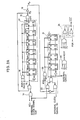
- Figs. 1A and 1B are block diagrams showing an entire construction of an embodiment of the present invention.
- An IC card 1 has an external terminal set 2. This external terminal set is used to electrically connect the IC card 1 to a terminal unit 30 when the card 1 is attached thereto.
- An external power, an external clock signal and an external reset signal are applied from the terminal unit 30 through respective terminals 2a, 2b and 2c of the external terminal set 2. Those external power, the external clock signal and the external reset signal are applied to a clock switching circuit 3.
- An internal oscillation circuit 4 is provided to generate an internal clock signal.
- the clock switching circuit 3 switches between an internal clock signal generated from the internal oscillation circuit 4 and the external clock signal inputted through the external terminal set 2 and applies the signal selected by the switching to an internal circuit 5.
- electric power is supplied from a battery 28 to the clock switching circuit 3, the internal oscillation circuit 4 and the internal circuit 5.
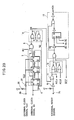
- Figs. 2A and 2B are specific definite electric circuit diagrams of the embodiment of the invention.
- a counter 17 is provided to output signals Q ⁇ 4 and Q ⁇ 5 for outputting a signal ⁇ p of a low (L) level from a NAND gate 18 and a signal ⁇ p of a high (H) level from an inverter 19 in response to the count of a predetermined number of pulses of an external clock signal f out .
- a switching circuit 20 is used to switch between an internal clock signal f in and the external clock signal f out in response to the signal ⁇ p, so that either clock signal is outputted as a system clock ⁇ to the internal circuit 5 shown in Fig. 1 and to a counter 21.
- the counter 21 is provided to output signals F1 to F4 for forming timing signals ACLR and ACL′ by means of gates 22 and 23 and a latch circuit 24.
- a counter circuit 7 is reset by an external clock signal f out , counts pulses of the internal clock signal f in and generates timing signals ARQ0 to ARQ2 for forming a signal AR.
- a latch circuit 12 is latched by an external reset signal and it is reset by a signal ACLR which attains H level after several cycles from the switching from the internal clock signal f in to the external clock signal f out .
- a synchronizing circuit 13 is provided to generate a signal ACL1 which synchronizes the output of the latch circuit 12 with clock signals ⁇ 3 and ⁇ 4 generated from the system clock ⁇ .
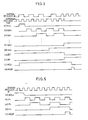
- Figs. 3, 4 and 5 are timing charts for explaining a definite operation of this embodiment.
- a power supply switch (not shown) provided in the IC card 1 is operated and then a power-on reset signal POR is applied to a reset input terminal of the counter 17 through an OR gate 16 shown in Fig. 2A, whereby the counter 17 is reset.
- the power-on reset signal POR is also applied to the counter 21 through an OR gate 25, whereby the counter 21 is reset.
- the outputs Q ⁇ 4 and Q ⁇ 5 of the counter 17 are lowered to L level and the respective outputs are supplied to the NAND gate 18.
- the signal ⁇ p outputted from the NAND gate 18 rises to H level and it is applied to one input terminal of the NAND gate 15. In consequence, this NAND gate 15 is opened. Further, the signal ⁇ p is inverted by the inverter 19 to the signal ⁇ p of L level, which is applied to the switching circuit 20. In response to this signal ⁇ p, the switching circuit 20 selects the internal clock signal f in and outputs this signal as the system clock pulse ⁇ to the internal circuit 5 shown in Fig. 1. Then, in response to the system clock pulse ⁇ , the internal circuit 5 carries out predetermined operation.
- the external power, the external clock signal f out and the external reset signal are applied from the terminal unit 30 to the external terminal set 2 of the card 1.
- the external reset signal of L level is inverted by the inverter 10 as shown in Fig. 2B and it is supplied as the signal ACL of H level to the OR circuit 11 as shown in (c) of Fig. 3.
- the OR circuit 11 outputs a signal ACLx of H level and in response to this signal, the latch circuit 12 is latched.
- the output of the latch circuit 12 is supplied to the synchronizing circuit 13 and the synchronizing circuit 13 synchronizes the clock pulses ⁇ 3 and ⁇ 4 with the output of the latch circuit 12 and outputs the signal ACL1 as shown in (j) of Fig. 3.
- This signal ACL1 is applied to one input terminal of the NAND gate 14.
- the NAND gate 14 is opened.
- the external clock signal f out as shown in Fig. (b) of Fig. 3 is applied to the other input terminal of the NAND gate 14.
- the external clock signal f out is applied to the NAND gate 15 through the NAND gate 14.
- the counter 17 is reset by the application of the signal ACLx outputted from the OR circuit 11 shown in Fig. 2B through the OR circuit 16 and, as shown in (f) and (g) of Fig. 3, the outputs Q ⁇ 4 and Q ⁇ 5 are respectively at L level.
- the signal ⁇ p outputted from the NAND gate 18 rises to H level as shown in (h) of Fig. 3, so that the NAND gate 15 is opened.
- the external clock signal f out is applied to the counter 17 through the NAND gate 15.
- the counter 17 starts counting pulses of the external clock signal f out .
- the signal ⁇ p of L level is inverted by the inverter 19 to H level and the signal of H level is applied to the switching circuit 20.
- the switching circuit 20 outputs the external clock signal f out as the system clock ⁇ to the internal circuit 5.
- the system clock ⁇ is applied to the counter 21, so that the counter 21 outputs the timing signals F1 to F3 as shown in (c), (d) and (e) of Fig. 5.
- the AND gate 22 outputs the signal ACLR of H level as shown in (k) of Fig. 3 and (f) of Fig. 5 and the latch circuit 12 shown in Fig. 2B is reset by the signal ACLR.
- the synchronizing circuit 13 When the latch circuit 12 is reset, the synchronizing circuit 13 outputs the signal ACL1 falling to L level as shown in (j) of Fig. 3.
- the NAND gate 14 is closed by the signal ACL1 and the external clock signal f out is not applied to the NAND 15.
- the signal ACL1 is used to enable the internal circuit 5. More specifically, the internal circuit 5 is initialized in a period of H level of the signal ACL1 and after the signal ACL1 falls to L level, the internal circuit 5 operates. Thus, as shown in (j) of Fig. 3, since the signal ACL1 falls to L level after several cycles from the switching from the internal clock signal f in to the external clock signal f out , the internal circuit 5 operates stably and erroneous operation can be prevented.
- the switching circuit 20 selects the internal clock signal f in and outputs it to the internal circuit 5.
- the IC card 1 is forcedly ejected from the terminal unit 30, switching occurs from the external clock signal f out to the internal clock signal f in and thereafter the signal ACL1 falls to L level, whereby the internal circuit 5 starts operation.
- the IC card when the IC card is attached to a terminal unit, pulses of the external clock signal supplied from the terminal unit are counted and, in response to counting of a predetermined number of pulses of the external clock signal, the external clock signal is selected and outputted in place of the internal clock signal. Accordingly, it can be correctly determined whether the IC card is operated in the form of a single body or in the form attached to any terminal unit.
Abstract
Description
- The present invention relates to a clock signal switching device of an IC card. More particularly, the present invention relates to a clock signal switching device of an IC card for switching from an internal clock signal to an external clock signal supplied from a terminal unit, whereby an IC card operable in response to the internal clock signal can operate by the external clock signal in place of the internal clock signal when the IC card is attached to the terminal unit.
- IC cards provided with displays are utilized in various fields these days. Such an IC card is operable not only as a single body of a card but also in the form attached to a terminal unit. For those purposes, an IC card contains a battery, an internal clock signal generating circuit for generating an internal clock signal, and a processing circuit and, in the form of the single body of the card, the processing circuit operates in response to the internal clock signal.
- When such a card is attached to a terminal unit, an external power is supplied from the terminal unit to the IC card and an external clock signal is also supplied thereto. The processing circuit in the IC card operates in response to the external clock signal. Thus, switching between the clock signals is required to apply the internal clock signal when the IC card is to operate in the form of a single body and to apply the external clock signal when an IC card is attached to the terminal unit. For those purposes, it is necessary to determine whether the IC card is operated as a single body or it is connected to a terminal unit. Methods for such determination include a method of detecting a mechanical contact of an external terminal provided in the IC card, and a method of detecting a difference between the voltage of the battery contained in the IC card and that of the internal power supplied when the card is attached to the terminal unit.
- However, in view of the structure of an IC card in general, it is difficult to attach a detector to its external terminal for the purpose of detecting the above mentioned mechanical contact. The method of detecting the difference of the voltages cannot be always utilized, for example, in cases in which there is only a small difference between the voltage of the battery contained in the IC card and the voltage of the external power supply, and when a noise is mixed in the case of using the IC card as a single body, it is often erroneously determined that the card is attached to a terminal unit, causing errors in operation.
- If an IC card is forcedly ejected from the terminal unit during communication of data between the card and the terminal unit, switching from the external clock signal to the internal clock signal occurs abruptly, causing a disorder in the program contained in the IC card.
- Therefore, a principal object of the present invention is to provide a clock signal switching device of an IC card, which can be operated stably irrespective of whether the IC card is utilized as a single body or it is attached to a terminal unit.
- Briefly stated, according to the present invention, in an IC card which contains containing a battery and a clock signal generating circuit for generating an internal clock signal and operates in response to the internal clock signal and to which electric power and an external clock signal are supplied from a terminal unit when it is attached to the terminal unit, pulses of the external clock signal supplied from the terminal unit are counted and in response to the count of a predetermined number of pulses of the external clock signal, the external clock signal is selected and outputted in place of the internal clock signal.
- Therefore, according to the present invention, it can be correctly determined whether the IC card is operated as a single body or it is attached to a terminal unit.
- In a preferred embodiment of the present invention, an internal clock signal is outputted in place of the external clock signal after an elapse of a predetermined period in response to detection of no input of the external clock signal and input of the internal clock signal.
- Consequently, according to the preferred embodiment of the invention, the internal clock signal is selected after the elapse of the predetermined period after the external clock signal is not inputted, and accordingly an abrupt change from the external clock signal to the internal clock signal does not occur and there is no fear of disorder in the program contained in the IC card.
- The foregoing and other objects, features, aspects and advantages of the present invention will become more apparent from the following detailed description of the present invention when taken in conjunction with the accompanying drawings.
-
- Figs. 1A and 1B are block diagrams showing an entire construction of an embodiment of the present invention.
- Figs. 2A and 2B are specific electric diagrams of the embodiment of the present invention.
- Figs. 3, 4 and 5 are timing charts for explaining operation of the embodiment of the present invention.
- Figs. 1A and 1B are block diagrams showing an entire construction of an embodiment of the present invention.
- Referring first to Figs. 1A and 1B, the construction of the embodiment of the invention will be described. An
IC card 1 has anexternal terminal set 2. This external terminal set is used to electrically connect theIC card 1 to aterminal unit 30 when thecard 1 is attached thereto. An external power, an external clock signal and an external reset signal are applied from theterminal unit 30 throughrespective terminals external terminal set 2. Those external power, the external clock signal and the external reset signal are applied to aclock switching circuit 3. Aninternal oscillation circuit 4 is provided to generate an internal clock signal. Theclock switching circuit 3 switches between an internal clock signal generated from theinternal oscillation circuit 4 and the external clock signal inputted through theexternal terminal set 2 and applies the signal selected by the switching to aninternal circuit 5. When theIC card 1 is not attached to theterminal unit 30, electric power is supplied from abattery 28 to theclock switching circuit 3, theinternal oscillation circuit 4 and theinternal circuit 5. - Figs. 2A and 2B are specific definite electric circuit diagrams of the embodiment of the invention.
- Referring first to Fig. 2A, a
counter 17 is provided to output signals Qφ4 and Qφ5 for outputting a signalφp of a low (L) level from aNAND gate 18 and a signal φp of a high (H) level from aninverter 19 in response to the count of a predetermined number of pulses of an external clock signal fout. Aswitching circuit 20 is used to switch between an internal clock signal fin and the external clock signal fout in response to the signal φp, so that either clock signal is outputted as a system clock φ to theinternal circuit 5 shown in Fig. 1 and to acounter 21. Thecounter 21 is provided to output signals F1 to F4 for forming timing signals ACLR andACL′ by means ofgates latch circuit 24. - Referring to Fig. 2B, a
counter circuit 7 is reset by an external clock signalfout , counts pulses of the internal clock signal fin and generates timing signals ARQ0 to ARQ2 for forming a signal AR. Alatch circuit 12 is latched by an external reset signal and it is reset by a signal ACLR which attains H level after several cycles from the switching from the internal clock signal fin to the external clock signal fout. A synchronizingcircuit 13 is provided to generate a signal ACL1 which synchronizes the output of thelatch circuit 12 with clock signals φ3 and φ4 generated from the system clock φ. - Figs. 3, 4 and 5 are timing charts for explaining a definite operation of this embodiment.
- Referring to Figs. 2A to 5, the definite operation of the embodiment will be described. First, in the case of operating the
IC card 1 singly without being attached to theterminal unit 30, a power supply switch (not shown) provided in theIC card 1 is operated and then a power-on reset signal POR is applied to a reset input terminal of thecounter 17 through anOR gate 16 shown in Fig. 2A, whereby thecounter 17 is reset. The power-on reset signal POR is also applied to thecounter 21 through anOR gate 25, whereby thecounter 21 is reset. In consequence, the outputs Qφ4 and Qφ5 of thecounter 17 are lowered to L level and the respective outputs are supplied to theNAND gate 18. The signalφp outputted from theNAND gate 18 rises to H level and it is applied to one input terminal of theNAND gate 15. In consequence, this NANDgate 15 is opened. Further, the signalφp is inverted by theinverter 19 to the signal φp of L level, which is applied to theswitching circuit 20. In response to this signal φp, theswitching circuit 20 selects the internal clock signal fin and outputs this signal as the system clock pulse φ to theinternal circuit 5 shown in Fig. 1. Then, in response to the system clock pulse φ, theinternal circuit 5 carries out predetermined operation. - Next, operation in the case of attaching the
IC card 1 to theterminal unit 30 will be described. When theIC card 1 is attached to theterminal unit 30, the external power, the external clock signal fout and the external reset signal are applied from theterminal unit 30 to theexternal terminal set 2 of thecard 1. The external reset signal of L level is inverted by theinverter 10 as shown in Fig. 2B and it is supplied as the signal ACL of H level to theOR circuit 11 as shown in (c) of Fig. 3. The ORcircuit 11 outputs a signal ACLx of H level and in response to this signal, thelatch circuit 12 is latched. The output of thelatch circuit 12 is supplied to the synchronizingcircuit 13 and the synchronizingcircuit 13 synchronizes the clock pulses φ3 and φ4 with the output of thelatch circuit 12 and outputs the signal ACL1 as shown in (j) of Fig. 3. This signal ACL1 is applied to one input terminal of theNAND gate 14. As a result, theNAND gate 14 is opened. The external clock signal fout as shown in Fig. (b) of Fig. 3 is applied to the other input terminal of theNAND gate 14. The external clock signal fout is applied to theNAND gate 15 through theNAND gate 14. - At this time, the
counter 17 is reset by the application of the signal ACLx outputted from theOR circuit 11 shown in Fig. 2B through theOR circuit 16 and, as shown in (f) and (g) of Fig. 3, the outputs Qφ4 and Qφ5 are respectively at L level. In consequence, the signalφp outputted from theNAND gate 18 rises to H level as shown in (h) of Fig. 3, so that theNAND gate 15 is opened. As a result, the external clock signal fout is applied to thecounter 17 through theNAND gate 15. The counter 17 starts counting pulses of the external clock signal fout. When a predetermined number of pulses of the external clock signal fout are counted, that is, when the outputs Qφ4 and Qφ5 of thecounter 17 rise to H level, the signalφp outputted from theNAND gate 18 falls to L level, whereby theNAND gate 15 is closed. As a result, the external clock signal fout is not applied to thecounter 17. Thus, thecounter 17 stops counting pulses of the external clock signal fout. - On the other hand, the signal
φp of L level is inverted by theinverter 19 to H level and the signal of H level is applied to the switchingcircuit 20. In response to the signalφp , the switchingcircuit 20 outputs the external clock signal fout as the system clock φ to theinternal circuit 5. At the same time, the system clock φ is applied to thecounter 21, so that thecounter 21 outputs the timing signals F1 to F3 as shown in (c), (d) and (e) of Fig. 5. When all of the timing signals F1 to F3 attain H level, the ANDgate 22 outputs the signal ACLR of H level as shown in (k) of Fig. 3 and (f) of Fig. 5 and thelatch circuit 12 shown in Fig. 2B is reset by the signal ACLR. When thelatch circuit 12 is reset, the synchronizingcircuit 13 outputs the signal ACL1 falling to L level as shown in (j) of Fig. 3. TheNAND gate 14 is closed by the signal ACL1 and the external clock signal fout is not applied to theNAND 15. - The signal ACL1 is used to enable the
internal circuit 5. More specifically, theinternal circuit 5 is initialized in a period of H level of the signal ACL1 and after the signal ACL1 falls to L level, theinternal circuit 5 operates. Thus, as shown in (j) of Fig. 3, since the signal ACL1 falls to L level after several cycles from the switching from the internal clock signal fin to the external clock signal fout, theinternal circuit 5 operates stably and erroneous operation can be prevented. - Referring now to the timing chart of Fig. 4, description will be made of the case in which the
IC card 1 is forcedly removed from theterminal unit 30. When theIC card 1 is removed from theterminal unit 30, the external clock signal fout is no longer applied. On this occasion, the input terminal for the external clock signal fout is pulled up by aresistor 26 as shown in Fig. 2B and accordingly it is raised to H level. The signal of H level at this terminal is inverted by theinverter 27 and it is applied to the reset input terminal of thecounter 7, whereby the counter starts counting pulses of the internal clock signal fin shown in (a) of Fig. 4. When the signals ARQ0 and ARQ2 of thecounter 7 both rise to H level and the signal φp rises to H level as shown in (b) and (d) of Fig. 4, thelatch circuit 9 is latched and the signal AR outputted from thelatch circuit 9 rises to H level as shown in (e) of Fig. 4. This signal AR is inputted to theOR circuit 11 and the signal ACLx outputted from theOR circuit 11 rises to H level as shown in (g) of Fig. 4, whereby thelatch circuit 12 is latched. - When the signal ACLx rises to H level, the
counters NAND gate 18 outputs the signalφp of H level, while theinverter 19 outputs the signal φp of L level as shown in (h) of Fig. 4. In consequence, the switchingcircuit 20 selects the internal clock signal fin and outputs it to theinternal circuit 5. Thus, when theIC card 1 is forcedly ejected from theterminal unit 30, switching occurs from the external clock signal fout to the internal clock signal fin and thereafter the signal ACL1 falls to L level, whereby theinternal circuit 5 starts operation. - As described in the foregoing, according to the embodiment of the present invention, when the IC card is attached to a terminal unit, pulses of the external clock signal supplied from the terminal unit are counted and, in response to counting of a predetermined number of pulses of the external clock signal, the external clock signal is selected and outputted in place of the internal clock signal. Accordingly, it can be correctly determined whether the IC card is operated in the form of a single body or in the form attached to any terminal unit.
- Although the present invention has been described and illustrated in detail, it is clearly understood that the same is by way of illustration and example only and is not to be taken by way of limitation, the spirit and scope of the present invention being limited only by the terms of the appended claims.
Claims (7)
clock signal counting means (17) for counting pulses of said external clock signal supplied when said IC card is attached to said terminal unit, and
clock signal switching means (20) for selecting and outputting said external clock signal in place of said internal clock signal when said clock signal counting means counts a predetermined number of pulses of said external clock signal.
input clock signal detecting means for detecting no input of said external clock signal and input of said internal clock signal,
said clock signal switching means comprising means for outputting said internal clock signal in place of said external clock signal after an elapse of a predetermined time in response to the detection of no input of said external clock signal and input of said internal clock signal by said input clock signal detecting means.
said IC card contains a processing circuit (5), and said clock signal switching means comprises
determining means (18) for determining that said clock signal counting means counts the predetermined number of pulses of the clock signal, and
enable signal generating means (21, 22) for outputting an enable signal for enabling said processing circuit after an elapse of a predetermined time in response to the determination of said predetermined number of pulses of the clock signal by said determining means.
said IC card includes a terminal (2c) for receiving an external reset signal for resetting said processing circuit, and
said enable signal generating means includes means (13) for outputting said external reset signal as said enable signal in synchronization with said internal clock signal in response to application of said external reset signal.
Applications Claiming Priority (2)
| Application Number | Priority Date | Filing Date | Title |
|---|---|---|---|
| JP63087996A JPH0610830B2 (en) | 1988-04-09 | 1988-04-09 | IC card clock signal switching device |
| JP87996/88 | 1988-04-09 |
Publications (3)
| Publication Number | Publication Date |
|---|---|
| EP0337684A2 true EP0337684A2 (en) | 1989-10-18 |
| EP0337684A3 EP0337684A3 (en) | 1990-12-27 |
| EP0337684B1 EP0337684B1 (en) | 1995-07-19 |
Family
ID=13930410
Family Applications (1)
| Application Number | Title | Priority Date | Filing Date |
|---|---|---|---|
| EP89303478A Expired - Lifetime EP0337684B1 (en) | 1988-04-09 | 1989-04-07 | Clock signal switching device of an IC card |
Country Status (4)
| Country | Link |
|---|---|
| US (1) | US4968899A (en) |
| EP (1) | EP0337684B1 (en) |
| JP (1) | JPH0610830B2 (en) |
| DE (1) | DE68923475T2 (en) |
Cited By (5)
| Publication number | Priority date | Publication date | Assignee | Title |
|---|---|---|---|---|
| GB2321744A (en) * | 1997-01-30 | 1998-08-05 | Motorola Inc | Portable data carrier and method for selecting an operating mode thereof |
| WO2001061638A1 (en) * | 2000-02-17 | 2001-08-23 | Orga Kartensysteme Gmbh | Chip card for detecting measurement data |
| WO2001061639A1 (en) * | 2000-02-17 | 2001-08-23 | Orga Kartensysteme Gmbh | Chip card |
| WO2005109552A2 (en) * | 2004-04-30 | 2005-11-17 | Micronas Gmbh | Chip with a power supply device |
| DE102007039226A1 (en) | 2007-08-20 | 2009-02-26 | Giesecke & Devrient Gmbh | Real-time measurement on a portable data carrier |
Families Citing this family (11)
| Publication number | Priority date | Publication date | Assignee | Title |
|---|---|---|---|---|
| JP2723296B2 (en) * | 1989-06-06 | 1998-03-09 | 株式会社東芝 | Portable media |
| US5313619A (en) * | 1991-05-16 | 1994-05-17 | Gerard J. Severance | External clock unit for a computer |
| US5155443A (en) * | 1990-12-19 | 1992-10-13 | Emhart Industries, Inc. | Machine for inspecting the wall thickness of glass containers |
| JPH04336308A (en) * | 1991-05-13 | 1992-11-24 | Nec Corp | Single-chip microcomputer |
| US5483185A (en) * | 1994-06-09 | 1996-01-09 | Intel Corporation | Method and apparatus for dynamically switching between asynchronous signals without generating glitches |
| US5801561A (en) * | 1995-05-01 | 1998-09-01 | Intel Corporation | Power-on initializing circuit |
| JP3493096B2 (en) * | 1996-06-07 | 2004-02-03 | 株式会社東芝 | Semiconductor integrated circuit, IC card, and IC card system |
| DE10057477B4 (en) * | 2000-11-20 | 2007-05-24 | Sagem Orga Gmbh | smart card |
| US7081780B2 (en) * | 2004-06-01 | 2006-07-25 | Randall Don Briggs | Reset circuitry for an integrated circuit |
| JP5166927B2 (en) * | 2007-06-12 | 2013-03-21 | ルネサスエレクトロニクス株式会社 | Processing equipment |
| JP5742910B2 (en) * | 2013-10-23 | 2015-07-01 | 大日本印刷株式会社 | IC chip, IC card, and method of operating IC chip |
Citations (6)
| Publication number | Priority date | Publication date | Assignee | Title |
|---|---|---|---|---|
| GB2080585A (en) * | 1980-07-22 | 1982-02-03 | Tokyo Shibaura Electric Co | Semiconductor integrated circuit with reduced power consumption |
| JPS60173949A (en) * | 1984-02-20 | 1985-09-07 | Fujitsu Ltd | Clock supply system |
| JPS61236240A (en) * | 1985-04-12 | 1986-10-21 | Nec Corp | Clock selection system for decentralized type processing unit |
| US4651277A (en) * | 1983-09-16 | 1987-03-17 | Sanyo Electric Co., Ltd. | Control system for a magnetic disk drive unit |
| FR2596897A1 (en) * | 1986-04-08 | 1987-10-09 | Casio Computer Co Ltd | INTEGRATED CIRCUIT CARD AND SYSTEM USING SAME |
| EP0257648A2 (en) * | 1986-08-29 | 1988-03-02 | Kabushiki Kaisha Toshiba | Portable medium |
Family Cites Families (4)
| Publication number | Priority date | Publication date | Assignee | Title |
|---|---|---|---|---|
| JPS59193366A (en) * | 1983-04-19 | 1984-11-01 | Ricoh Co Ltd | Apparatus for detecting momentary interruption of ac power source |
| EP0160163B1 (en) * | 1984-04-02 | 1988-06-08 | Mitsubishi Denki Kabushiki Kaisha | Variable frequency power source operating system |
| US4675539A (en) * | 1985-09-17 | 1987-06-23 | Codex Corporation | Backup power system |
| US4850000A (en) * | 1987-11-05 | 1989-07-18 | Dallas Semiconductor Corporation | Gated shift register |
-
1988
- 1988-04-09 JP JP63087996A patent/JPH0610830B2/en not_active Expired - Fee Related
-
1989
- 1989-04-07 EP EP89303478A patent/EP0337684B1/en not_active Expired - Lifetime
- 1989-04-07 DE DE68923475T patent/DE68923475T2/en not_active Expired - Lifetime
- 1989-04-07 US US07/334,566 patent/US4968899A/en not_active Expired - Lifetime
Patent Citations (6)
| Publication number | Priority date | Publication date | Assignee | Title |
|---|---|---|---|---|
| GB2080585A (en) * | 1980-07-22 | 1982-02-03 | Tokyo Shibaura Electric Co | Semiconductor integrated circuit with reduced power consumption |
| US4651277A (en) * | 1983-09-16 | 1987-03-17 | Sanyo Electric Co., Ltd. | Control system for a magnetic disk drive unit |
| JPS60173949A (en) * | 1984-02-20 | 1985-09-07 | Fujitsu Ltd | Clock supply system |
| JPS61236240A (en) * | 1985-04-12 | 1986-10-21 | Nec Corp | Clock selection system for decentralized type processing unit |
| FR2596897A1 (en) * | 1986-04-08 | 1987-10-09 | Casio Computer Co Ltd | INTEGRATED CIRCUIT CARD AND SYSTEM USING SAME |
| EP0257648A2 (en) * | 1986-08-29 | 1988-03-02 | Kabushiki Kaisha Toshiba | Portable medium |
Non-Patent Citations (4)
| Title |
|---|
| IBM TECHNICAL DISCLOSURE BULLETIN. vol. 20, no. 11B, April 1978, NEW YORK US pages 4889 - 4890; D. S. Garriss: "Switchable clock generator" * |
| IBM TECHNICAL DISCLOSURE BULLETIN. vol. 26, no. 10A, March 1984, NEW YORK US pages 5260 - 5261; M.D. Brown and D.D. Reetz: "Integrated LSSD clock and reset control" * |
| PATENT ABSTRACTS OF JAPAN vol. 10, no. 11 (E-374) 17 January 1986, & JP-A-60 173949 (FUJITSU KK) 07 September 1985, * |
| PATENT ABSTRACTS OF JAPAN vol. 11, no. 81 (E-488) 12 March 1987, & JP-A-61 236240 (NEC CORP.) 21 October 1986, * |
Cited By (9)
| Publication number | Priority date | Publication date | Assignee | Title |
|---|---|---|---|---|
| GB2321744A (en) * | 1997-01-30 | 1998-08-05 | Motorola Inc | Portable data carrier and method for selecting an operating mode thereof |
| GB2321744B (en) * | 1997-01-30 | 2000-05-17 | Motorola Inc | Portable data carrier and method for selecting operating mode thereof |
| US6138918A (en) * | 1997-01-30 | 2000-10-31 | Motorlola, Inc. | Portable data carrier and method for selecting operating mode thereof |
| WO2001061638A1 (en) * | 2000-02-17 | 2001-08-23 | Orga Kartensysteme Gmbh | Chip card for detecting measurement data |
| WO2001061639A1 (en) * | 2000-02-17 | 2001-08-23 | Orga Kartensysteme Gmbh | Chip card |
| WO2005109552A2 (en) * | 2004-04-30 | 2005-11-17 | Micronas Gmbh | Chip with a power supply device |
| WO2005109552A3 (en) * | 2004-04-30 | 2007-04-05 | Micronas Gmbh | Chip with a power supply device |
| CN100552703C (en) * | 2004-04-30 | 2009-10-21 | 迈克纳斯公司 | Chip with electric supply installation |
| DE102007039226A1 (en) | 2007-08-20 | 2009-02-26 | Giesecke & Devrient Gmbh | Real-time measurement on a portable data carrier |
Also Published As
| Publication number | Publication date |
|---|---|
| JPH0610830B2 (en) | 1994-02-09 |
| DE68923475T2 (en) | 1996-02-15 |
| EP0337684A3 (en) | 1990-12-27 |
| EP0337684B1 (en) | 1995-07-19 |
| JPH01259480A (en) | 1989-10-17 |
| US4968899A (en) | 1990-11-06 |
| DE68923475D1 (en) | 1995-08-24 |
Similar Documents
| Publication | Publication Date | Title |
|---|---|---|
| US4968899A (en) | Clock signal switching device of an IC Card | |
| KR920005171A (en) | Semiconductor memory with successively clocked call codes for entering test mode | |
| KR920005167A (en) | Semiconductor memory with multiple clocks for entering test mode | |
| US5632680A (en) | Method and apparatus for controlling a computer game | |
| US4384326A (en) | Memory security circuit using the simultaneous occurance of two signals to enable the memory | |
| KR920003446B1 (en) | Output circuit for producing positive and negative pulse at a single output terminal | |
| EP0158512A2 (en) | Reset circuit | |
| JPH0129093B2 (en) | ||
| EP0022458B1 (en) | Hierarchical computer system for entrance control | |
| EP3595174A2 (en) | Comparator circuit with feedback and method of operation | |
| KR19980042277A (en) | Low delay and high reliability input signal readout circuit | |
| US3843893A (en) | Logical synchronization of test instruments | |
| US4198579A (en) | Input circuit for portable electronic devices | |
| JP3813994B2 (en) | Difference capture timer | |
| US4365203A (en) | Multi-frequency clock generator with error-free frequency switching | |
| US4887071A (en) | Digital activity loss detector | |
| US5966034A (en) | Method and device for the filtering of a pulse signal | |
| US4010423A (en) | Multi-function remote control ic | |
| EP0005946A1 (en) | Time-period comparing device | |
| SU1049838A1 (en) | Device for checking integrated circuit | |
| KR100365406B1 (en) | Auto reset circuit for Liquid Crystal Display controller | |
| KR0128249Y1 (en) | Dose counter display circuit | |
| EP0570143B1 (en) | Method and apparatus for interfacing a serial data signal | |
| JP2556038B2 (en) | Hybrid integrated circuit | |
| KR910006702Y1 (en) | Apparatus for measuring stability of clock pulses by using first-in-first-out register |
Legal Events
| Date | Code | Title | Description |
|---|---|---|---|
| PUAI | Public reference made under article 153(3) epc to a published international application that has entered the european phase |
Free format text: ORIGINAL CODE: 0009012 |
|
| AK | Designated contracting states |
Kind code of ref document: A2 Designated state(s): DE FR GB |
|
| PUAL | Search report despatched |
Free format text: ORIGINAL CODE: 0009013 |
|
| AK | Designated contracting states |
Kind code of ref document: A3 Designated state(s): DE FR GB |
|
| 17P | Request for examination filed |
Effective date: 19901214 |
|
| 17Q | First examination report despatched |
Effective date: 19930210 |
|
| GRAA | (expected) grant |
Free format text: ORIGINAL CODE: 0009210 |
|
| AK | Designated contracting states |
Kind code of ref document: B1 Designated state(s): DE FR GB |
|
| REF | Corresponds to: |
Ref document number: 68923475 Country of ref document: DE Date of ref document: 19950824 |
|
| ET | Fr: translation filed | ||
| PLBE | No opposition filed within time limit |
Free format text: ORIGINAL CODE: 0009261 |
|
| STAA | Information on the status of an ep patent application or granted ep patent |
Free format text: STATUS: NO OPPOSITION FILED WITHIN TIME LIMIT |
|
| 26N | No opposition filed | ||
| REG | Reference to a national code |
Ref country code: GB Ref legal event code: IF02 |
|
| PGFP | Annual fee paid to national office [announced via postgrant information from national office to epo] |
Ref country code: DE Payment date: 20080411 Year of fee payment: 20 Ref country code: FR Payment date: 20080312 Year of fee payment: 20 |
|
| PGFP | Annual fee paid to national office [announced via postgrant information from national office to epo] |
Ref country code: GB Payment date: 20080409 Year of fee payment: 20 |
|
| REG | Reference to a national code |
Ref country code: GB Ref legal event code: PE20 Expiry date: 20090406 |
|
| PG25 | Lapsed in a contracting state [announced via postgrant information from national office to epo] |
Ref country code: GB Free format text: LAPSE BECAUSE OF EXPIRATION OF PROTECTION Effective date: 20090406 |