EP0335748A2 - Recording mode identifying circuit and a reproducing apparatus comprising the same - Google Patents
Recording mode identifying circuit and a reproducing apparatus comprising the same Download PDFInfo
- Publication number
- EP0335748A2 EP0335748A2 EP89303233A EP89303233A EP0335748A2 EP 0335748 A2 EP0335748 A2 EP 0335748A2 EP 89303233 A EP89303233 A EP 89303233A EP 89303233 A EP89303233 A EP 89303233A EP 0335748 A2 EP0335748 A2 EP 0335748A2
- Authority
- EP
- European Patent Office
- Prior art keywords
- signal
- mode
- reproduced
- level
- luminance signal
- Prior art date
- Legal status (The legal status is an assumption and is not a legal conclusion. Google has not performed a legal analysis and makes no representation as to the accuracy of the status listed.)
- Granted
Links
Images


Classifications
-
- H—ELECTRICITY
- H04—ELECTRIC COMMUNICATION TECHNIQUE
- H04N—PICTORIAL COMMUNICATION, e.g. TELEVISION
- H04N9/00—Details of colour television systems
- H04N9/79—Processing of colour television signals in connection with recording
- H04N9/80—Transformation of the television signal for recording, e.g. modulation, frequency changing; Inverse transformation for playback
- H04N9/82—Transformation of the television signal for recording, e.g. modulation, frequency changing; Inverse transformation for playback the individual colour picture signal components being recorded simultaneously only
- H04N9/83—Transformation of the television signal for recording, e.g. modulation, frequency changing; Inverse transformation for playback the individual colour picture signal components being recorded simultaneously only the recorded chrominance signal occupying a frequency band under the frequency band of the recorded brightness signal
-
- H—ELECTRICITY
- H04—ELECTRIC COMMUNICATION TECHNIQUE
- H04N—PICTORIAL COMMUNICATION, e.g. TELEVISION
- H04N9/00—Details of colour television systems
- H04N9/79—Processing of colour television signals in connection with recording
- H04N9/87—Regeneration of colour television signals
-
- H—ELECTRICITY
- H04—ELECTRIC COMMUNICATION TECHNIQUE
- H04N—PICTORIAL COMMUNICATION, e.g. TELEVISION
- H04N9/00—Details of colour television systems
- H04N9/79—Processing of colour television signals in connection with recording
- H04N9/80—Transformation of the television signal for recording, e.g. modulation, frequency changing; Inverse transformation for playback
- H04N9/82—Transformation of the television signal for recording, e.g. modulation, frequency changing; Inverse transformation for playback the individual colour picture signal components being recorded simultaneously only
- H04N9/83—Transformation of the television signal for recording, e.g. modulation, frequency changing; Inverse transformation for playback the individual colour picture signal components being recorded simultaneously only the recorded chrominance signal occupying a frequency band under the frequency band of the recorded brightness signal
- H04N9/832—Transformation of the television signal for recording, e.g. modulation, frequency changing; Inverse transformation for playback the individual colour picture signal components being recorded simultaneously only the recorded chrominance signal occupying a frequency band under the frequency band of the recorded brightness signal using an increased bandwidth for the luminance or the chrominance signal
- H04N9/833—Transformation of the television signal for recording, e.g. modulation, frequency changing; Inverse transformation for playback the individual colour picture signal components being recorded simultaneously only the recorded chrominance signal occupying a frequency band under the frequency band of the recorded brightness signal using an increased bandwidth for the luminance or the chrominance signal with selection of the conventional or the increased bandwidth signal, e.g. VHS or SVHS signal selection
-
- H—ELECTRICITY
- H04—ELECTRIC COMMUNICATION TECHNIQUE
- H04N—PICTORIAL COMMUNICATION, e.g. TELEVISION
- H04N9/00—Details of colour television systems
- H04N9/79—Processing of colour television signals in connection with recording
- H04N9/87—Regeneration of colour television signals
- H04N9/898—Regeneration of colour television signals using frequency multiplication of the reproduced colour signal carrier with another auxiliary reproduced signal, e.g. a pilot signal carrier
Abstract
Description
- This invention relates to detecting the mode of a reproduced colour video signal, and more particularly to recording mode identifying circuits suitable for use in a magnetic recording and/or reproducing apparatus capable of selective operation in a low-band mode and a high-band mode, and to apparatus for reproducing a colour video signal.
- In a rotary video tape recorder (VTR) of the type in which a luminance signal is frequency modulated (FM) and a chroma signal is down-converted to a low frequency region for recording in oblique tracks on a magnetic tape, horizontal resolution can be improved, and consequently high picture quality can be achieved, by increasing the carrier frequency that is frequency modulated by the luminance signal. Therefore, it has been recommended that a VTR be provided with a mode in which recording is carried out with the carrier freqeuncy used for frequency modulating the luminance signal higher than the carrier frequency usually used in such a VTR.
- Thus in the recording format of an 8-mm VTR, the carrier frequency for the frequency modulation by the luminance signal is usually set to be 4.2 MHz at the sync tip level and 5.4 MHz at the white peak level, and it has been suggested that recording be performed with a higher carrier frequency, that is, with a carrier frequency which is 5.7 MHz at the sync tip level and 7.7 MHz at the white peak level.
- If a mode in which the carrier freqeuncy for the frequency modulation by the luminance signal is increased, hereinafter called the "high-band mode", is to be selectively established in a VTR in addition to a usually employed mode which is hereinafter called the "low-band mode", then in a reproducing operation of the VTR, it is necessary to change the characteristic of a luminance signal processing circuit in correspondence with the mode used when the tape was recorded. More specifically, it is necessary to change the sensitivity of an FM demodulator or a characteristic of a low-pass filter provided after the FM demodulator in accordance with whether the high-band mode or the low-band mode was used in recording the tape being reproduced. It is troublesome to switch such characteristics of the VTR manually for the various modes, and, when changed manually, correct mode setting cannot be reliably achieved in the case where a mode transition occurs intermediate the ends of the tape.
- For the above reasons, a VTR equipped with a mode identifying circuit has been proposed for automatically determining whether the video signal was recorded on the reproduced tape in the low-band mode or the high-band mode. Such a mode identifying circuit detects a signal level of a predetermined frequency component which is concentrated in a recorded signal of one mode, and determines whether this detection level is equal to, or above a predetermined level, as the basis for a mode identification.
- An example of such a mode identification circuit is shown in Figure 1 in which a reproduced FM luminance signal YFM is supplied from an
input terminal 100 to a band-pass filter 101 which passes a frequency component of a frequency fL which is included in the FM luminance signal YFM and corresponds, for example, to the sync tip level of the video signal when recorded in the low-band mode. It will be appreciated that the frequency component which corresponds to the carrier frequency fL of the FM luminance signal for the sync tip level of the reproduced FM luminance signal YFM can be picked up when reproducing a low-band recording. The output of the band-pass filter 101 is supplied to adetector 102 which detects the level of the frequency component corresponding to the carrier frequency fL. The output of thedetector 102 is applied to a negative input of acomparator 103 which receives a reference voltage at a positive input thereof. Thecomparator 103 detects whether the output level of thedetector 102 is equal to or greater than the predetermined reference voltage, and the resulting output of thecomparator 103 is available at anoutput terminal 104 as a mode identifying output. - With this circuit, if the reproduced FM luminance signal YFM is a low-band signal, the output level of the
detector 102 becomes equal to or greater than the reference voltage. As a result, the output of thecomparator 103 assumes a negative or low level. When the reproduced FM luminance signal, YFM is a high-band signal, it is intended that no signal equal to or larger than the reference voltage is detected at thedetector 102, and that, as a result thereof, the output of thecomparator 103 will assume a high level for identifying the high-band signal. - Figure 2 shows another example of a proposed mode identifying circuit in which the reproduced FM luminance signal is supplied from an
input terminal 110 to a band-pass filter 111 which, for example, passes the frequency component fL corresponding to the sync tip level in the case of the low-band mode, and also to a band-pass filter 112 which, for example, passes a frequency component FH corresponding to the sync tip level in the case of the high-band mode. The output of the band-pass filter 111 is supplied to adetector 113, and the output of thedetector 113 is applied to a negative input of acomparator 115. The output of the band-pass filter 112 is supplied to adetector 114, and the output of thedetector 114 is reapplied to a positive input of thecomparator 115. The resulting output of thecomparator 115 is made available at anoutput terminal 116 as a mode identifying signal. - If the reproduced FM luminance signal is a low-band signal, usually the output level of the
detector 113 is larger than the output level of thedetector 114, so that the output of thecomparator 115 is a negative or low level signal for identifying the low-band signal. When the reproduced FM luminance signal YFM is a high-band signal, usually the output of thedetector 114 is larger than the output of thedetector 113 and, therefore, the output of thecomparator 115 is at a high level to identify the high-band signal. - However, if the signal level of a predetermined frequency component concentrated in a reproduced FM luminance signal YFM which had been recorded in a low-band mode, or the signal level of a predetermined frequency component concentrated in a reproduced FM luminance signal YFM which had been recorded in a high-band mode is detected, as in Figures 1 and 2, and the reproducing mode is switched or changed-over in response to such detected level, there is a possibility that an erroneous mode identification will occur due to the influence of sideband components.
- More specifically, in the circuit of Figure 1, it is intended that an output equal to or greater than a predetermined value is obtained from the
detector 102 only if the reproduced FM luminance signal YFM was recorded in the low-band mode, whereas, if the reproduced FM luminance signal YFM was recorded in the high-band mode, it is assumed that the output from thedetector 102 will be clearly less than the predetermined value represented by the reference voltage supplied to the positive input of thecomparator 103. However, in actual practice, even if the reproduced FM luminance signal YFM was recorded in the high-band mode, its lower sideband may coincide with, or include the carrier frequency corresponding to the sync tip level of the low-band mode. In this case, a frequency component of the lower sideband is passed by the band-pass filter 101, and a signal equal to or greater than the predetermined level may be detected at thedetector 102. Therefore, the output of thecomparator 103 may assume a low level despite the fact that the reproduced FM luminance signal YFM was recorded in the high-band mode, and it is erroneously indicated that the video signal being reproduced was recorded in the low-band mode. - Similarly, in the circuit of Figure 2, even when the reproduced FM luminance signal YFM was recorded in the high-band mode, its lower sideband may be in the vicinity of the frequency fL characteristic of the carrier frequency for the sync tip level in the low-band mode and which is a pass band of the band-
pass filter 111, and, if the level of the lower sideband at the frequency fL is larger than the level of the carrier at the frequency fH, the output level of thedetector 113 is larger than that of thedetector 114. As a result, the output of thecomparator 115 assumes a low level, so that there is an erroneous indication of the low band mode. - In order to prevent such erroneous mode indication, it has been proposed, for example, as shown in Figure 3, to provide a
gate circuit 106 between theinput terminal 100 and the band-pass filter 101 in Figure 1, for transmitting the reproduced FM luminance signal only during each synchronization signal interval, in response to a gating pulse GP suitably supplied to aterminal 107. Thus, a predetermined frequency component of the reproduced FM luminance signal YFM during each synchronization signal interval is detected for identifying the mode used for recording the reproduced video signal. - Since the level of the luminance signal is constant during each synchronization interval, the carrier of the FM luminance signal during each synchronization signal interval has a predetermined frequency and its sideband components are spread in a predetermined manner. As a result, by thus detecting the predetermined frequency component in the reproduced FM luminance signal YFM only during each synchronization interval for identifying the recording mode, only a carrier component of the low-band mode can be detected, and an erroneous mode identification due to the influence of the lower sideband component of a reproduced FM luminance signal recorded in the high-band mode can be prevented.
- However, in order to detect the reproduced FM luminance signal YFM only during the synchronization signal interval, it is necessary to develop the gate pulse GP corresponding to the synchronization period and supply the gate pulse GP to the
terminal 107. The foregoing requires separation of a synchronization signal from a demodulated and reproduced luminance signal for the development of the gate pulse GP. However, an FM demodulator for demodulating the reproduced FM luminance signal YFM cannot produce a correct demodulated output unless the demodulator is properly set in conformity with the mode used in recording. For this reason, at a time when the recording mode has not yet been identified, the synchronization signal cannot be separated from the reproduced FM luminance signal YFM and the gate pulse GP cannot be readily formed. - According to the present invention there is provided a recording mode identifying circuit for determining whether a reproduced FM signal is of a first mode in which recording is effected with frequency modulation of a first carrier frequency by an information signal or of a second mode in which recording is effected with frequency modulation of a second carrier frequency by the information signal, said mode identifying circuit being characterized by:
phase inverting means for inverting a predetermined frequency component of a reproduced FM signal which corresponds to the frequency of the carrier of one of said first and second modes when modulated by a predetermined information signal level;
limiter means for eliminating an amplitude component of an output of said phase inverting means; and
level detecting means for detecting a level of said predetermined frequency component in the reproduced FM signal which has had said predetermined frequency component inverted and said amplitude component eliminated, whereby the mode with which said reproduced FM signal was recorded is determined from said level detected by said level detecting means. - According to the present invention there is also provided an apparatus for reproducing a colour video signal composed of a luminance signal and a chroma signal, and which is recorded on a magnetic tape according to a first mode in which recording is effected with frequency modulation of a first carrier frequency by said luminance signal or according to a second mode in which recording is effected with frequency modulation of a second carrier frequency by said luminance signal, said apparatus comprising:
magnetic head means for reproducing said colour video signal recorded on the magnetic tape;
separation circuit means for separating the reproduced colour video signal from said magnetic head means into an FM luminance signal and a chroma signal;
processing circuit means for processing the separated chroma signal;
FM demodulation means which is selectively operative in first and second modes for demodulating the separated FM luminance signal when the colour video signal is recorded in said first and second modes, respectively; and
de-emphasis means for de-emphasizing the demodulated luminance signal from said FM demodulating means;
characterized by:
a recording mode identifying circuit for determining whether said reproduced colour video signal is of said first mode or said second mode, including phase inverting means for inverting a predetermined frequency component of a separated FM luminance signal which corresponds to the frequency of the carrier of one of said first and second modes when modulated by a predetermined luminance signal level, limiter means for eliminating an amplitude component of an output of said phase inverting means, and level detecting means for detecting a level of said predetermined frequency component in the separated FM luminance signal which has had said predetermined frequency component inverted and said amplitude component eliminated, whereby the mode with which said reproduced colour video signal was recorded is determined from said level detected by said level detecting means; and
system control means responsive to a determination that the reproduced colour video signal was recorded with said first and second modes, respectively, for selectively operating said FM demodulating means in said first and second modes, respectively. - In accordance with an embodiment of this invention, a recording mode identifying circuit, for example, for use in a magnetic recording and/or reproducing apparatus capable of recording a colour video signal in a first or low-band mode in which a luminance signal is recorded as a frequency modulation of a first carrier frequency and a second or high-band mode in which the luminance signal is recorded as a frequency modulation of a second carrier frequency; comprises a phase inverter for inverting a predetermined frequency component of a reproduced FM luminance signal which corresponds to the frequency of the carrier of one of the modes when modulated by a predetermined luminance signal level, for example, the frequency component of the lower sideband corresponding to the sync tip level in the low-band mode, a limiter eliminating an amplitude component of the output of the phase inverter, and a level detector for detecting a level of said predetermined frequency component in the reproduced FM luminance signal which has had said predetermined frequency component inverted and said amplitude component eliminated, whereby the mode with which the reproduced signal was recorded is determined from the level detected by said level detector.
- In a preferred embodiment of the invention, the phase inverter includes band-pass filter means receiving said reproduced FM luminance signal and arranged to pass said predetermined frequency component thereof, amplifying means receiving said predetermined frequency component passed by said band-pass filter means and operative to effect a two-fold amplification thereof, and subtracting means for subtracting the two-fold or doubly amplified predetermined frequency component from said reproduced FM luminance signal and, as a result thereof, providing the reproduced FM luminance signal with the phase of said predetermined frequency component inverted therein.
- In a particular embodiment in which the recording mode is identified from the level of a frequency component of the reproduced FM luminance signal corresponding to the carrier frequency f₁ for a sync tip level recorded in a low-band mode; the phase of the component of the frequency f₁ of the reproduced FM luminance signal is inverted and its amplitude component is eliminated. In such case, if the lower sideband of the high-band mode includes the frequency f₁, the lower sideband of the high-band mode at the frequency f₁ is suppressed. In this way, the level of the frequency component f₁ of the reproduced FM luminance signal whose lower sideband in the high-band mode is suppressed at the frequency f₁ is detected for identifying the recording mode. Since the lower sideband in the high-band mode at the frequency f₁ is suppressed, an erroneous identification of the mode due to the influence of sideband components can be prevented.
- The invention will now be described by way of example with reference to the accompanying drawings, throughout which like parts are referred to by like references, and in which:
- Figures 1 to 3 are block diagrams of respective previously proposed mode identifying circuits;
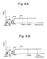
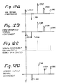
- Figures 4A and 4B show frequency spectra for recording in low-band and high-band modes, respectively;
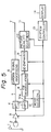
- Figure 5 is a block diagram showing a VTR reproducing system to which an embodiment of the invention is applied;
- Figure 6 is a spectrum diagram to which reference is made in explaining characteristics of an FM signal;
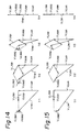
- Figure 7 is a vector diagram to which reference is made in further explaining the FM signal;
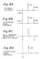
- Figure 8A to 8D are spectra diagrams to which reference will be made in explaining operating principles;
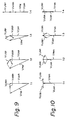
- Figures 9, 10 and 11 are vector diagrams to which reference will be made in further explaining the operating principles;
- Figures 12A to 12D are spectra diagrams to which reference will be made in further explaining the operating principles;
- Figures 13, 14 and 15 are vector diagrams to which reference will be made in further explaining operating principles;
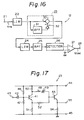
- Figure 16 is a block diagram showing an embodiment of mode identifying circuit according to the invention; and
- Figure 17 is a circuit diagram showing a specific arrangement of a phase inverting circuit in the circuit of Figure 16.
- Various aspects of an embodiment of this invention will now be described under the following headings:
- a. Structure of a VTR reproducing system to which the invention is applied
- b. Explanation of operating principles of an example of a mode identifying circuit
- c. Structure of one example of the mode identifying circuit
- d. General arrangement of a phase inverting circuit
- e. Particular structure of the phase inverting circuit
- f. Examples of application of the invention.
- The invention can advantageously be applied to a VTR in which a video signal recorded with a high-band, or a video signal recorded with a low-band can be selectively reproduced.
- Figure 4A is a spectrum of a signal recorded in a low-band mode in an 8-mm VTR, and Figure 4B is a spectrum of a signal recorded in a high-band mode in an 8-mm VTR. In Figures 4A and 4B, YFM is an FM luminance signal, C is a so-called down-converted chroma signal, AFM is an FM audio signal, and P is the spectrum of pilot signals for ATF tracking. In the low-band mode, the carrier frequency of the FM luminance signal YFM is selected so that, as shown in Figure 4A, a frequency of 4.2 MHz corresponds to the sync tip level and a frequency of 5.4 MHz corresponds to the white peak level. In the high-band mode, as shown in Figure 4B, the carrier frequency is selected so that the sync tip level is at a frequency of 5.7 MHz and the white peak level is at a frequency of 7.7 MHz. In both the low-band mode and the high-band mode, the centre frequency of the down-converted chroma signal is selected to be 743 kHz, and a centre frequency of the FM audio signal AFM is selected to be 1.5 MHz.
- Referring now to Figure 5, it will be seen that, in a reproducing system for a video signal in a VTR to which the present invention may be applied, a signal recorded on a
magnetic tape 1 is reproduced by a rotatedhead 2, and the reproduced signal is supplied to aregenerative amplifier 3 through a rotary transformer (not shown). The output of theamplifier 3 is supplied to a band-pass filter 4 and a high-pass filter 5. A reproduced down-converted chroma signal C is obtained from the output of the band-pass filter 4, and a reproduced FM luminance signal YFM is obtained from the output of the high-pass filter 5. - The reproduced down-converted chroma signal C is supplied to a chroma
signal processing circuit 6 in which, for example, time-axis variations of the reproduced signal and cross-talk components are eliminated. Moreover, in theprocessing circuit 6, the reproduced down-converted chroma signal C is returned to a chroma signal having a standard sub-carrier frequency, for example, of 3.58 MHz. A processed chroma signal is supplied from the output of theprocessing circuit 6 to anoutput terminal 7. - A reproduced FM luminance signal YFM obtained from the band-pass filter 5 is supplied to an
FM demodulator 8 where a luminance signal is derived. The output of thedemodulator 8 is supplied through ade-emphasis circuit 9 and a picture-quality adjusting circuit 10 to arespective output terminal 11. - In the VTR of Figure 5, as mentioned before, it is possible to establish recording in a high-band mode in which the picture quality is improved through the use of an increased carrier frequency at the time of frequency modulation of a luminance signal, or to effect recording in the usual low-band mode. The FM luminance signal YFM separated by the high-pass filter 5 is supplied to a
mode identifying circuit 12 which determines whether the signal being reproduced from thetape 1 was recorded in the high-band mode or the low-band mode. The output of themode identifying circuit 12, which identifies the recording mode, is supplied to theregenerative amplifier 3, theFM demodulator 8, thede-emphasis circuit 9, and the picture-quality-adjusting circuit 10, respectively, for controlling or changing-over theregenerative amplifier 3, theFM demodulator 8, thede-emphasis circuit 9, and the picture-quality-adjusting circuit 10 so that the characteristics thereof will at all times be suitable to accommodate the reproduced signal whether the latter was recorded in the low-band mode or the high-band mode as indicated by the output from themode identifying circuit 12. - The output of the
mode identifying circuit 12 is also supplied to asystem controller 13, for example, in the form of a microprocessor. An output of thesystem controller 13 is applied to adisplay unit 14, so that the mode in which the signal was recorded on thetape 1 being played-back or reproduced is displayed on thedisplay unit 14. On the basis of such display, a user can readily ascertain which recording mode was employed for the recording in on thetape 1. - The
mode identifying circuit 12 relies for its operation on the fact that the carrier frequencies are different for recording in the low-band mode and for recording in the high-band mode. - In one form of the
mode identifying circuit 12, the level of a frequency component of the reproduced FM luminance signal having a frequency f₁ corresponding to the sync tip level at the time of low-band recording is detected and the mode identification is effected on the basis of whether the frequency component of the frequency f₁ is equal to or larger than a predetermined level. However, as earlier noted, in such case, it is necessary to avoid the erroneous mode identification which may occur when the frequency range of the lower sideband of the FM luminance signal recorded in high-band mode includes the frequency f₁. - Therefore, in this case the lower sideband component of the frequency f₁ present in the reproduced FM luminance signal which was recorded in the high-band mode is substantially eliminated, whereupon the level of the component of the frequency f₁ can be detected without the possibility of error. Generally, the lower sideband component of the frequency f₁ in a reproduced FM luminance signal which was recorded in the high-band mode is suppressed by inverting the phase of the component of the frequency f₁ and eliminating a resulting amplitude component by a limiter.
- In other words, an FM signal may be represented as follows:
f(t) = Ao [Jo(mf) sinωot
+J₁(mf) (sin (ωo + p)t - sin (ωo - p)t)
+J₂(mf) (sin (ωo + 2p)t + sin (ωo - 2p)t)
+J₃(mf) (sin (ωo + 3p)t - sin (ωo - 3 p)t)
+ ....]
where
ωo is the angular velocity of the carrier
p is the angular velocity of the signal wave
mf is the modulation index - From the above equation, an FM signal can be represented by a spectrum diagram as shown in Figure 6, and in which the sidebands spread upward and downward from the carrier CAR as a centre. Among these sideband components, the first-order sidebands LSB1 and USB1, and the third-order sidebands LSB3 and USB3, which are sidebands of an odd-number order, are made so that their upper sidebands and lower sidebands are inverted in respect to one another. The second-order sideband components LSB2 and USB2, and the fourth-order sideband components LSB4 and USB4, which are sidebands of an even-number order, are made so that their upper sidebands and lower sidebands have the same phase as each other.
- Furthermore, from the above equation, the FM signal may be represented by the vector diagram of Figure 7 which shows an FM signal vector FFM over its second-order sideband component. A carrier vector Vcar is rotated with the angular velocity ωo; a first-order upper sideband vector VUSB1 is rotated with the angular velocity p; a first-order lower sideband vector VLSB1 is rotated with an angular velocity -p; a second-order upper sideband vector VUSB2 is rotated with an angular velocity 2p; and a second-order lower sideband vector VLSB2 is rotated with an angular velocity -2p.
- It is assumed, for example, as shown in Figure 8A, that the first-order lower sideband LSB1 of the high-band mode coincides with the frequency f₁ for the purposes of this explanation of how the first-order sideband LSB1 with the frequency f₁ can be suppressed by eliminating an amplitude component after inverting the component of the frequency f₁. Similar explanations can be provided for the cases where the lower sidebands LSB1, LSB3 and LSB5, respectively, of an odd-number order coincide with the frequency f₁.
- It is further assumed, as shown in Figure 8A, that the first-order sidebands LSB1 and USB1 of the FM signal are inverted with respect to each other.
- When the phase of the first-order lower sideband LSB1 of the FM signal shown in Figure 8A is inverted, the first-order upper sideband USB1 has the same phase as the lower first-order lower sideband LSB1 as shown in Figure 8B. As a result, by inverting the first-order sideband LSB1, an AM component is derived from the first-order sideband component.
- Such an AM component can be eliminated by amplitude limitation by a limiter. More specifically, when a signal with the spectrum shown in Figure 8B is applied to the limiter, and the AM component shown in Figure 8C is added equivalently, the upper sideband USB1 and the lower sideband LSB1 are suppressed, as shown in Figure 8D.
- The foregoing will be described in detail with reference to Figures 9, 10 and 11.
- As mentioned above, the carrier vector VCAR is rotated with the angular velocity ωo, the first-order upper sideband vector VUSB1 is rotated with the angular velocity p, and the first-order lower sideband VLSB1 is rotated with the angular velocity -p. As a result, the vector diagram of the FM signal over the first-order sideband at each of times t₁ to t₄ is as shown in Figure 9. It is to be noted that for facilitating understanding, only the first-order upper sideband vector VUSB1 and the first order lower sideband VLSB1 are shown to be rotated and the carrier vector VCAR is shown in a fixed position in the drawing, that is, not rotated.
- As shown in Figure 9, the length of the FM signal vector VFM hardly varies at the times t₁ to t₄ when the first-order sideband vectors VLSB1 and VUSB1 are small. In other words, the amplitude of the FM signal barely changes.
- On the other hand, when the first-order lower sideband LSB1 is inverted, the vector VFM1 of a signal at each of the times t₁ to t₄ has an amplitude component that is substantially influenced by the first-order sideband, as indicated in Figure 10. In other words, the length of the signal vector VFM1 is different at each of the times t₁ to t₄.
- With the elimination of the amplitude component of this signal by means of the limiter, as shown in Figure 11, the first-order upper sideband USB1 and the inverted first-order lower sideband LSB1 are eliminated so as to provide only a vector VLIM corresponding to a carrier vector CAR.
- Next, it will be explained how the second-order sideband LSB2 present in the frequency f₁ can be suppressed by eliminating an amplitude component after inversion of the component of the frequency f₁ when the second-order lower sideband LSB2 of the signal recorded with high-band mode coincides with the frequency f₁. Similar explanations can be provided for the cases where the lower sidebands of an even-number order LSB2, LSB4 .... coincides with the frequency f₁.
- It is assumed for the purpose of this explanation that the second-order sideband LSB2 of the FM signal coincides with the frequency f₁, and that the second-order sidebands LSB2 and USB2 of the FM signal have the same phase, as shown in Figure 12A.
- Upon inversion of the second-order lower sideband LSB2 at the frequency F₁, the
upper sideband USB 2 and the lower sideband LSB2 have inverted phases with respect to each other. As a result, an amplitude component appears in the FM signal which is supplied to the limiter. In the limiter, a component shown in Figure 12C is added equivalently. Upon the equivalent addition of the signal having the spectrum shown in Figure 12C to the signal with the spectrum indicated in Figure 12B, a signal with the spectrum shown in Figure 12D is provided. Clearly, as shown in Figure 12D, the second-order lower sideband LSB2 is cancelled and the second-order upper sideband USB2 is increased two-fold. - The foregoing will be described in detail below with the reference to vector diagrams of Figures 13, 14 and 15.
- The FM signal over its second-order sideband may be represented by the vector diagram of Figure 13, in which the carrier vector VCAR is shown not rotated for facilitating understanding, thereof. As is apparent from Figure 13, the amplitude of the FM signal vector VFM hardly varies at the times t₁₁ to t₁₄.
- Upon the inverting of the second-order lower sideband vector VLSB2 of the FM signal shown in Figure 13, the signal vector VFM1 becomes as shown in Figure 14. More specifically, when the second-order lower sideband vector VLSB2 of the FM signal shown in Figure 13 is inverted, the vector VFM of a signal at the times t₁₁ to t₁₄ has an amplitude component since the lengths of the signal vector VFM1 at the times t₁₁ to t₁₄, respectively, are different from each other.
- The signal represented in Figure 14 is supplied to the limiter for the elimination of its amplitude component. In other words, as shown in Figure 15, an amplitude component is added so that a signal vector VLIM at each of the times t₁₁ to t₁₄ becomes almost constant. As a result, as indicated in Figure 15, the second-order lower sideband vector VLSB2 is cancelled and the second order upper sideband VUSB2 is increased two-fold.
- As earlier stated, the
mode identifying circuit 12 suppresses a sideband component having the frequency f₁ by inverting a signal component of the frequency corresponding to the sync tip level of the low-band mode, for example, and eliminating an amplitude component by means of a limiter, and then detects the signal level of the frequency f₁ as the basis for identifying the recording mode. - In the
mode identifying circuit 12 shown in Figure 16, a reproduced FM luminance signal YFM is supplied from aninput terminal 21 through alimiter 22 to aphase inverting circuit 23. Thephase inverting circuit 23 inverts only the phase of a predetermined frequency f₁, for example, the phase of a component having the frequency corresponding to the sync tip level in the low-band recording mode. Of course, the pedestal level may be used instead of the sync tip level. - The output of the
phase inverting circuit 23 is supplied to alimiter 24 in which amplitude components of the output of thephase inverting circuit 23 are eliminated. The output of thelimiter 24 is supplied to a band-pass filter 25. - In the case where the component of the frequency f₁ is a sideband, a circuit for suppressing such sideband is constituted by the
phase inverting circuit 23 and thelimiter 24. When the lower sideband of a reproduced video signal which was recorded in the high-band mode includes the frequency f₁ such lower sideband is suppressed by thephase inverting circuit 23 and thelimiter 24. - The band-
pass filter 25 permits passage of a component of a predetermined frequency, for example, the frequency f₁ corresponding to the sync tip level when recording with low-band mode. The output of the band-pass filter 25 is supplied to adetector 26 which detects the level of the component of the frequency f₁ of the reproduced FM luminance signal YFM through thelimiter 22, thephase inverting circuit 23 and thelimiter 24. - The output of the
detector 26 is applied to a negative input of acomparator 27. Thecomparator 27 detects whether the component level of the frequency f₁ of the reproduced FM luminance signal YFM obtained through thelimiter 22, thephase inverting circuit 23, thelimiter 24 and the band-pass filter 25 is equal to or above a predetermined reference level established by a reference voltage applied to a positive input of thecomparator 27. The output of thecomparator 27 is applied to anoutput terminal 28 as a mode identifying signal Mdet. - As noted above, the circuit for suppressing the sideband of the frequency f₁ is composed of the
phase inverting circuit 23 and thelimiter 24. More particularly, the component of the frequency f₁ is suppressed by thephase inverting circuit 23 and thelimiter 24 when the component of the frequency f₁ of the reproduced FM luminance signal is the lower sideband of the signal recorded in the high-band mode. As a result, only a carrier component of the frequency f₁ of the reproduced FM luminance signal YFM which corresponds to the low-band sync tip is detected at thedetector 26. - In the case where a reproduced video signal was recorded in the low-band mode, the carrier component of the frequency f₁ corresponding to the sync tip level of the low-band mode is produced and passes through the band-
pass filter 25 so that the output level of thedetector 26 is equal to or above the level of the reference voltage applied to the positive input of thecomparator 27. Thus, the mode identifying signal Mdet is at a low negative level when the reproduced video signal was recorded in the low-band mode. When the reproduced video signal was recorded in the high-band mode, the output level of thedetector 26 becomes substantially less than the predetermined value even if the lower sideband component of the frequency f₁ lies in the reproduced FM modulation luminance signal YFM. This is because the lower sideband of the FM luminance signal recorded in the high-band mode is suppressed by thephase inverting circuit 23 and thelimiter 24. Therefore, the output Mdet of thecomparator 27 is reliably at a high level when the reproduced video signal was recorded in the high-band mode. - The
phase inverting circuit 23 may be composed of a band-pass filter 31, anamplifier 32, and a subtractingcircuit 33, for example, as shown in Figure 16. The band-pass filter 31 has a characteristic which passes a predetermined frequency component, for instance, a frequency component of the frequency f₁ corresponding to the sync tip level, or alternatively to the pedestal level, when recording in low-band mode. Theamplifier 32 has a gain of two. - The reproduced FM luminance signal, after being limited by the
limiter 22, is supplied to a positive input of the subtractingcircuit 33 and through the band-pass filter 31 to theamplifier 32. The component of the predetermined frequency f₁ of the reproduced FM luminance signal is passed by the band-pass filter 31, and the component of the frequency f₁ is then doubly amplified by theamplifier 32. The doubly or two-fold amplified component of the frequency f₁ is supplied to an inverted input of the subtractingcircuit 33. - Components of the reproduced FM luminance signal YFM of frequencies other than the frequency f₁ are supplied directly, that is, without alteration, through the subtracting
circuit 33. The component of the reproduced FM luminance signal YFM having the frequency f₁ is directly supplied to the subtractingcircuit 33, and also amplified doubly by theamplifier 32 before being applied to the negative or inverting input of the subtractingcircuit 33. Therefore, the doubly amplified component of the frequency f₁ is subtracted from the component of the frequency f₁ of the reproduced FM luminance signal YFM applied directly to the positive input of the subtractingcircuit 33. Consequently, the component of the frequency f₁ of the reproduced FM luminance signal YFM is inverted at the output of the subtractingcircuit 33. - Figure 17 shows a practical circuit arrangement for the
phase inverting circuit 23, and in which the base of atransistor 41 is connected through acapacitor 42 to aninput terminal 43.Resistances earth terminal 45. A junction between the series connectedresistances transistor 41. - The collector of the
transistor 41 is connected to the power supply terminal 44 through aresistance 50, and the collector of thetransistor 41 is further connected to one end of a series connection of acoil 48 and avariable capacitor 49. The band-pass filter 31 in Figure 16 for passing the frequency component of the predetermined frequency f₁ is composed of thecoil 48 and thecapacitor 49. The emitter of thetransistor 41 is connected to theearth terminal 45 through aresistance 51 and also is connected to one end of aresistance 52 which, at its other end, is connected to the base of atransistor 53. The other end of the series connection of thecoil 48 and thecapacitor 49 is also connected to the base of thetransistor 53. The collector of thetransistor 53 is connected to the power supply terminal 44, and the emitter of thetransistor 53 is coupled to theearth terminal 45 through aresistance 54. The emitter of thetransistor 52 is further connected to anoutput terminal 55. - The reproduced FM luminance signal YFM is supplied to the base of the
transistor 41 from theinput terminal 43. Such FM signal is supplied from the emitter of thetransistor 41, and the FM signal is inverted and supplied from the collector of thetransistor 41. The gain of the signal output from the collector of thetransistor 41 is determined by theresistances - The FM signal derived at the emitter of the
transistor 41 is supplied to the base of thetransistor 53 through theresistance 52. The inverted FM signal provided at the collector of thetransistor 41 is also supplied to the base of thetransistor 53 through the band-pass filter consisting of thecoil 48 and thecapacitor 49. Therefore, an FM signal whose component of the frequency f₁ is inverted is provided at the emitter of thetransistor 53, and hence at theoutput terminal 55. - In the above described embodiment, the carrier frequency corresponding to the sync tip level is selected to be 4.2 MHz and the carrier frequency corresponding to the white peak level is selected to be 5.4 MHz in the low-band mode (Figure 4A), whereas, the carrier frequency corresponds to the sync tip level is selected to be 5.7 MHz and the carrier frequency corresponding to the white peak level is selected to be 7.7 MHz in the high-band mode (Figure 4B). However, this invention is also applicable to the cases where other carrier frequencies are used. For example, the invention can be similarly applied to the case where the carrier frequency for the sync tip level is selected to be 4.4 MHz and the carrier frequency for the white peak level is selected to be 5.6 MHz in the low-band mode, which is one example of a standard for a 1/2-inch VTR, while the carrier frequency for the sync tip level is selected to be 6.8 MHz and that for the white peak level is selected to be 8.6 MHz in the high-band mode.
- Another example to which the invention can be applied is the case where the carrier frequency for the sync tip level is selected to be 3.4 MHz and that for the white peak level is selected to be 4.4 MHz in the low-band mode (which is another example of a standard for a 1/2-inch VTR), while the carrier freqeuncy for the sync tip level is selected to be 5.4 MHz and that for the white peak level is selected to be 7.0 MHz in the high-band mode.
Claims (10)
phase inverting means (23) for inverting a predetermined frequency component of a reproduced FM signal which corresponds to the frequency of the carrier of one of said first and second modes when modulated by a predetermined information signal level;
limiter means (24) for eliminating an amplitude component of an output of said phase inverting means (23); and
level detecting means (26) for detecting a level of said predetermined frequency component in the reproduced FM signal which has had said predetermined frequency component inverted and said amplitude component eliminated, whereby the mode with which said reproduced FM signal was recorded is determined from said level detected by said level detecting means (26).
magnetic head means for reproducing said colour video signal recorded on the magnetic tape;
separation circuit means for separating the reproduced colour video signal from said magnetic head means into an FM luminance signal and a chroma signal;
processing circuit means for processing the separated chroma signal;
FM demodulation means which is selectively operative in first and second modes for demodulating the separated FM luminance signal when the colour video signal is recorded in said first and second modes, respectively; and
de-emphasis means for de-emphasizing the demodulated luminance signal from said FM demodulating means;
characterized by:
a recording mode identifying circuit for determining whether said reproduced colour video signal is of said first mode or said second mode, including phase inverting means for inverting a predetermined frequency component of a separated FM luminance signal which corresponds to the frequency of the carrier of one of said first and second modes when modulated by a predetermined luminance signal level, limiter means for eliminating an amplitude component of an output of said phase inverting means, and level detecting means for detecting a level of said predetermined frequency component in the separated FM luminance signal which has had said predetermined frequency component inverted and said amplitude component eliminated, whereby the mode with which said reproduced colour video signal was recorded is determined from said level detected by said level detecting means; and
system control means responsive to a determination that the reproduced colour video signal was recorded with said first and second modes, respectively, for selectively operating said FM demodulating means in said first and second modes, respectively.
Applications Claiming Priority (2)
| Application Number | Priority Date | Filing Date | Title |
|---|---|---|---|
| JP80387/88 | 1988-04-01 | ||
| JP63080387A JP2611320B2 (en) | 1988-04-01 | 1988-04-01 | Mode discrimination circuit |
Publications (3)
| Publication Number | Publication Date |
|---|---|
| EP0335748A2 true EP0335748A2 (en) | 1989-10-04 |
| EP0335748A3 EP0335748A3 (en) | 1991-11-21 |
| EP0335748B1 EP0335748B1 (en) | 1995-01-11 |
Family
ID=13716878
Family Applications (1)
| Application Number | Title | Priority Date | Filing Date |
|---|---|---|---|
| EP89303233A Expired - Lifetime EP0335748B1 (en) | 1988-04-01 | 1989-03-31 | Recording mode identifying circuit and a reproducing apparatus comprising the same |
Country Status (7)
| Country | Link |
|---|---|
| US (1) | US5032925A (en) |
| EP (1) | EP0335748B1 (en) |
| JP (1) | JP2611320B2 (en) |
| KR (1) | KR970003474B1 (en) |
| CA (1) | CA1313257C (en) |
| DE (1) | DE68920465T2 (en) |
| ES (1) | ES2066845T3 (en) |
Cited By (1)
| Publication number | Priority date | Publication date | Assignee | Title |
|---|---|---|---|---|
| EP0440167A2 (en) * | 1990-01-31 | 1991-08-07 | Sony Corporation | Recording mode discrimination circuit |
Families Citing this family (8)
| Publication number | Priority date | Publication date | Assignee | Title |
|---|---|---|---|---|
| SG73978A1 (en) * | 1990-01-31 | 2000-07-18 | Sony Corp | Recording mode discrimination circuit |
| KR940005841B1 (en) * | 1991-08-23 | 1994-06-24 | 주식회사 금성사 | Video control signal generator and controlling method thereof |
| JP3109185B2 (en) * | 1991-11-12 | 2000-11-13 | ソニー株式会社 | Digital VTR |
| JP3158614B2 (en) * | 1992-03-26 | 2001-04-23 | ソニー株式会社 | Digital demodulator |
| US5493346A (en) * | 1992-07-03 | 1996-02-20 | Sony Corporation | Signal demodulating apparatus capable of effectively suppressing the beat interference caused by the pilot signal |
| US5838875A (en) * | 1993-02-05 | 1998-11-17 | Goldstar Co., Ltd. | Apparatus and method for discriminating between analog and digital video signals in high definition video cassette recorder |
| KR100188921B1 (en) * | 1994-07-26 | 1999-06-01 | 김광호 | Shortly hi-band recording modulation circuit of 8mm vtr |
| KR100195107B1 (en) * | 1996-06-28 | 1999-06-15 | 윤종용 | Video signal dubbing recording apparatus |
Citations (1)
| Publication number | Priority date | Publication date | Assignee | Title |
|---|---|---|---|---|
| US4686585A (en) * | 1984-02-13 | 1987-08-11 | Sony Corporation | VTR having automatic carrier detection |
Family Cites Families (5)
| Publication number | Priority date | Publication date | Assignee | Title |
|---|---|---|---|---|
| US3764739A (en) * | 1971-01-25 | 1973-10-09 | Y Faroudja | Color video recording and play back system |
| JPS53114608A (en) * | 1977-03-16 | 1978-10-06 | Matsushita Electric Ind Co Ltd | Defect detector |
| JPS61127292A (en) * | 1984-11-27 | 1986-06-14 | Sony Corp | Trap circuit |
| KR890004853B1 (en) * | 1985-01-28 | 1989-11-29 | 미쓰비시전기 주식회사 | Circuits for processing video signals |
| JPS62291276A (en) * | 1986-06-11 | 1987-12-18 | Victor Co Of Japan Ltd | Discriminating device for recording mode of reproducing video signal |
-
1988
- 1988-04-01 JP JP63080387A patent/JP2611320B2/en not_active Expired - Lifetime
-
1989
- 1989-03-29 US US07/330,317 patent/US5032925A/en not_active Expired - Lifetime
- 1989-03-31 ES ES89303233T patent/ES2066845T3/en not_active Expired - Lifetime
- 1989-03-31 DE DE68920465T patent/DE68920465T2/en not_active Expired - Fee Related
- 1989-03-31 EP EP89303233A patent/EP0335748B1/en not_active Expired - Lifetime
- 1989-03-31 KR KR1019890004172A patent/KR970003474B1/en not_active IP Right Cessation
- 1989-03-31 CA CA000595296A patent/CA1313257C/en not_active Expired - Lifetime
Patent Citations (1)
| Publication number | Priority date | Publication date | Assignee | Title |
|---|---|---|---|---|
| US4686585A (en) * | 1984-02-13 | 1987-08-11 | Sony Corporation | VTR having automatic carrier detection |
Cited By (3)
| Publication number | Priority date | Publication date | Assignee | Title |
|---|---|---|---|---|
| EP0440167A2 (en) * | 1990-01-31 | 1991-08-07 | Sony Corporation | Recording mode discrimination circuit |
| EP0440167A3 (en) * | 1990-01-31 | 1992-03-18 | Sony Corporation | Recording mode discrimination circuit |
| US5223945A (en) * | 1990-01-31 | 1993-06-29 | Sony Corporation | Recording mode discrimination circuit |
Also Published As
| Publication number | Publication date |
|---|---|
| EP0335748B1 (en) | 1995-01-11 |
| EP0335748A3 (en) | 1991-11-21 |
| US5032925A (en) | 1991-07-16 |
| CA1313257C (en) | 1993-01-26 |
| JPH01253869A (en) | 1989-10-11 |
| ES2066845T3 (en) | 1995-03-16 |
| KR970003474B1 (en) | 1997-03-18 |
| DE68920465T2 (en) | 1995-06-14 |
| KR890016850A (en) | 1989-11-30 |
| JP2611320B2 (en) | 1997-05-21 |
| DE68920465D1 (en) | 1995-02-23 |
Similar Documents
| Publication | Publication Date | Title |
|---|---|---|
| US4622583A (en) | Audience rating measuring system | |
| JP2658147B2 (en) | Mode discrimination circuit | |
| US4686585A (en) | VTR having automatic carrier detection | |
| EP0335748B1 (en) | Recording mode identifying circuit and a reproducing apparatus comprising the same | |
| CA1043901A (en) | Control of automatic color control and color killer circuits in video signal reproducing apparatus | |
| US5121266A (en) | Magnetic recording/reproducing apparatus | |
| EP0287682B1 (en) | Apparatus for magnetically recording and reproducing video signals | |
| US4417284A (en) | Gain control circuit for a video tape recorder wherein the chrominance is gain controlled in response to the luminance signal as well as the chrominance signal | |
| EP0735539B1 (en) | Double deck video cassette tape recorder | |
| JP2811733B2 (en) | Magnetic recording / reproducing device | |
| JP2630866B2 (en) | Recording mode discrimination device for reproduced video signal | |
| JP2702250B2 (en) | Magnetic recording / reproducing device | |
| US5523855A (en) | Discriminating device for automatically discriminating between recorded video signal reproduction modes | |
| JPH06105534B2 (en) | Video recording / playback device | |
| JPS62291277A (en) | Mode discriminating device for recording medium reproducing device | |
| JPH0329165A (en) | Recording mode discriminating device | |
| JPS59108494A (en) | Pal secam signal discrimination circuit | |
| JPS63253781A (en) | Magnetic recording and reproducing device | |
| JPS63287280A (en) | Discriminating circuit | |
| JPH0740403B2 (en) | Recording mode detector | |
| JPS59147504A (en) | Fm signal demodulation circuit | |
| JPS62197964A (en) | Pcm processor built-in type video tape recorder | |
| JPH0325760A (en) | Device for discriminating recording system of frequency modulated video signal | |
| JPH0760567B2 (en) | Recording mode discrimination device | |
| JPH0312863A (en) | Device for discriminating recording system of frequency modulated video signal |
Legal Events
| Date | Code | Title | Description |
|---|---|---|---|
| PUAI | Public reference made under article 153(3) epc to a published international application that has entered the european phase |
Free format text: ORIGINAL CODE: 0009012 |
|
| AK | Designated contracting states |
Kind code of ref document: A2 Designated state(s): DE ES FR GB NL |
|
| PUAL | Search report despatched |
Free format text: ORIGINAL CODE: 0009013 |
|
| AK | Designated contracting states |
Kind code of ref document: A3 Designated state(s): DE ES FR GB NL |
|
| 17P | Request for examination filed |
Effective date: 19920321 |
|
| 17Q | First examination report despatched |
Effective date: 19940330 |
|
| GRAA | (expected) grant |
Free format text: ORIGINAL CODE: 0009210 |
|
| AK | Designated contracting states |
Kind code of ref document: B1 Designated state(s): DE ES FR GB NL |
|
| REF | Corresponds to: |
Ref document number: 68920465 Country of ref document: DE Date of ref document: 19950223 |
|
| REG | Reference to a national code |
Ref country code: ES Ref legal event code: FG2A Ref document number: 2066845 Country of ref document: ES Kind code of ref document: T3 |
|
| ET | Fr: translation filed | ||
| PLBE | No opposition filed within time limit |
Free format text: ORIGINAL CODE: 0009261 |
|
| STAA | Information on the status of an ep patent application or granted ep patent |
Free format text: STATUS: NO OPPOSITION FILED WITHIN TIME LIMIT |
|
| 26N | No opposition filed | ||
| REG | Reference to a national code |
Ref country code: GB Ref legal event code: IF02 |
|
| PGFP | Annual fee paid to national office [announced via postgrant information from national office to epo] |
Ref country code: FR Payment date: 20020312 Year of fee payment: 14 |
|
| PGFP | Annual fee paid to national office [announced via postgrant information from national office to epo] |
Ref country code: ES Payment date: 20020315 Year of fee payment: 14 |
|
| PGFP | Annual fee paid to national office [announced via postgrant information from national office to epo] |
Ref country code: GB Payment date: 20020327 Year of fee payment: 14 |
|
| PGFP | Annual fee paid to national office [announced via postgrant information from national office to epo] |
Ref country code: NL Payment date: 20020328 Year of fee payment: 14 |
|
| PGFP | Annual fee paid to national office [announced via postgrant information from national office to epo] |
Ref country code: DE Payment date: 20020404 Year of fee payment: 14 |
|
| PG25 | Lapsed in a contracting state [announced via postgrant information from national office to epo] |
Ref country code: GB Free format text: LAPSE BECAUSE OF NON-PAYMENT OF DUE FEES Effective date: 20030331 |
|
| PG25 | Lapsed in a contracting state [announced via postgrant information from national office to epo] |
Ref country code: ES Free format text: LAPSE BECAUSE OF NON-PAYMENT OF DUE FEES Effective date: 20030401 |
|
| PG25 | Lapsed in a contracting state [announced via postgrant information from national office to epo] |
Ref country code: NL Free format text: LAPSE BECAUSE OF NON-PAYMENT OF DUE FEES Effective date: 20031001 Ref country code: DE Free format text: LAPSE BECAUSE OF NON-PAYMENT OF DUE FEES Effective date: 20031001 |
|
| GBPC | Gb: european patent ceased through non-payment of renewal fee |
Effective date: 20030331 |
|
| PG25 | Lapsed in a contracting state [announced via postgrant information from national office to epo] |
Ref country code: FR Free format text: LAPSE BECAUSE OF NON-PAYMENT OF DUE FEES Effective date: 20031127 |
|
| NLV4 | Nl: lapsed or anulled due to non-payment of the annual fee |
Effective date: 20031001 |
|
| REG | Reference to a national code |
Ref country code: FR Ref legal event code: ST |
|
| REG | Reference to a national code |
Ref country code: ES Ref legal event code: FD2A Effective date: 20030401 |