EP0333594B1 - Direct memory access controller - Google Patents
Direct memory access controller Download PDFInfo
- Publication number
- EP0333594B1 EP0333594B1 EP89400746A EP89400746A EP0333594B1 EP 0333594 B1 EP0333594 B1 EP 0333594B1 EP 89400746 A EP89400746 A EP 89400746A EP 89400746 A EP89400746 A EP 89400746A EP 0333594 B1 EP0333594 B1 EP 0333594B1
- Authority
- EP
- European Patent Office
- Prior art keywords
- transfer
- control information
- data
- register
- memory access
- Prior art date
- Legal status (The legal status is an assumption and is not a legal conclusion. Google has not performed a legal analysis and makes no representation as to the accuracy of the status listed.)
- Expired - Lifetime
Links
Images


Classifications
-
- G—PHYSICS
- G06—COMPUTING; CALCULATING OR COUNTING
- G06F—ELECTRIC DIGITAL DATA PROCESSING
- G06F13/00—Interconnection of, or transfer of information or other signals between, memories, input/output devices or central processing units
- G06F13/14—Handling requests for interconnection or transfer
- G06F13/16—Handling requests for interconnection or transfer for access to memory bus
-
- G—PHYSICS
- G06—COMPUTING; CALCULATING OR COUNTING
- G06F—ELECTRIC DIGITAL DATA PROCESSING
- G06F13/00—Interconnection of, or transfer of information or other signals between, memories, input/output devices or central processing units
- G06F13/14—Handling requests for interconnection or transfer
- G06F13/20—Handling requests for interconnection or transfer for access to input/output bus
- G06F13/28—Handling requests for interconnection or transfer for access to input/output bus using burst mode transfer, e.g. direct memory access DMA, cycle steal
Landscapes
- Engineering & Computer Science (AREA)
- Theoretical Computer Science (AREA)
- Physics & Mathematics (AREA)
- General Engineering & Computer Science (AREA)
- General Physics & Mathematics (AREA)
- Bus Control (AREA)
Description
- The present invention generally relates to a direct memory access controller, and more particularly to a direct memory access controller capable of controlling a plurality of channels through which a direct memory access transfer is made.
- Recently, it is required to transfer a large amount of data such as image data with extremely high speed between a data processing system such as a personal computer or a workstation, and an external unit such as a disk unit. It is also required to transfer a large amount of data between memories provided in the system at an extremely high speed. A conventional data transfer is carried out under the control of a central processing unit (hereafter simply referred to as CPU) provided in the data processing apparatus. Therefore, the process speed of the conventional data transfer depends on the processing speed of the CPU. From this viewpoint, it is impossible to transfer data at a speed in excess of the processing speed of the CPU. Further, it takes long to transfer a large amount of data even when the data is low-speed data. From the above-mentioned viewpoints, a direct memory access transfer is used which enables it to be possible to transfer data between the data processing system and the external unit without using the CPU. Hereafter, direct memory access is simply referred to as DMA. A DMA controller which controls the DMA transfer is intended to effectively process a large amount of data and high-speed data.
- Generally, in the DMA controller, data is transferred in accordance with descriptors which are transfer control information necessary for the DMA transfer. Descriptors include a source address, a destination address, and a byte count (the number of bytes of data to be transferred). In the conventional DMA transfer, a plurality of types of DMA transfer are proposed. Examples of those are a register direct mode, and a descriptor chain mode, which is further classified into a sequential descriptor chain mode and a link descriptor chain mode.
- In the register direct mode, when a request for the DMA transfer occurs, the CPU releases a system bus from exclusive use, and then the DMA controller carries out the DMA transfer while exclusively using the system bus. At this time, various internal processing modes are processed in the DMA controller (this is called an internal process). For example, the DMA controller sets transfer control information which includes the source address, destination address and the byte count in internal registers. Then, after executing a predetermined error test, the DMA controller starts the data transfer based on the DMA transfer.
- Generally, the DMA controller is provided with a plurality of channels in order to cope with a plurality of requests of the DMA transfer. A channel is defined as a path between a device and a memory, or a path between memories. For example, a four-channel DMA controller is a DMA controller such that data transfers through four paths are simultaneously controlled. For example, image data for use in CRT display is transferred through a channel, and other data is transferred through one of the other channels. Of course, a plurality of data transfers cannot be made with respect to the system bus at the same time. Therefore, when two or more data transfers are requested at the same time, data relating to each of the requested channels is segmented into a plurality of unit-length data, which are alternately transferred by switching the channels. Thereby, the data transfers through a plurality of channels are carried out as if they are executed at the same time. It can can be seen from the above description that a reduction on channel switching time is very important to speed up the DMA transfer.
- However, in the conventional DMA controller, the response to the request of the DMA transfer is slow, because the conventional DMA transfer starts the data transfer operation after the internal process is completed. For example, transfer control information is generated in response to each transfer request, and is set in the corresponding registers. Then the present channel is switched to the requested channel. Thereafter, the DMA transfer is started. Therefore, there occurs a delay in response time from the occurrence of the transfer request to the start thereof. It is to be noted that most of the response time is taken to carry out the internal process. Additionally, the internal process is included in the processing time of the DMA transfer irrespective of the fact that the data transfer is not actually carried out during the internal process. Therefore, in the case where the channel switching is frequently carried out, the time taken to perform the internal process increases as the number of channel switching operations increases. As a result, the DMA transfer processing time increases, which prevents speeding up of the DMA transfer. Particularly, the DMA transfer is intended to transfer an extremely large amount of data for a short time. Consequently, it is required to reduce the response time for the DMA transfer request and speed up the entire data processing system.
- Finally, there is disclosed in JP-A-63 29868 a DMA controller having a basic configuration in which information concerning a memory block to be transferred is set up in a first memory address register, as recited in the preamble of
claim 1. At the the start of a present DMA transfer, a second memory address register is loaded with corresponding information for the next DMA data transfer to enhance transfer speed. - It is therefore a general object of the present invention to provide a novel and useful direct memory access controller in which the above-mentioned disadvantages of the conventional art are eliminated.
- A more specific object of the present invention is to provide a direct memory access controller in which transfer control information necessary for the next transfer request is generated beforehand, and is immediately output after the request of the above next DMA transfer request occurs. Thereby, it becomes possible to extremely reduce the response time and increases the DMA processing speed.
- The above objects of the present invention can be achieved by a direct memory access controller coupled to a system bus of a system for controlling data transfers through a plurality of channels by a direct memory access, comprising request handling means for receiving a transfer request generated by a device connected to the system bus; first register means for storing transfer control information used for obtaining transfer control information necessary for executing the data transfer by a next transfer request supplied from the request handling means; second register means for storing the transfer control information necessary for processing the next transfer request; transfer control information setting means for generating the transfer control information necessary for processing the next transfer request on the basis of the transfer control information registered in the first register means during the data transfer by the present transfer request and then renewing the first and second register means with the generated transfer control information; and transfer execution means for executing the actual data transfer through the system bus in accordance with the transfer control information registered in the second register means, which is output to the system bus therefrom.
- Other objects, features and advantages of the present invention will become apparent from the following detailed description when read in conjunction with the accompanying drawings.
-
- FIG.1 is a block diagram of a data processing system which employs a direct memory access controller in which there are formed a plurality of channels;
- FIG.2 is a block diagram illustrating the principle of the present invention;
- FIG.3 is a block diagram of an essential part of a preferred embodiment of the present invention;
- FIG.4 is a timing chart illustrating the operation of the embodiment of FIG.3;
- FIG.5 is a block diagram of the detailed structure for the block diagram of FIG.3; and
- FIG.6 is a timing chart illustrating the operation of the structure shown in FIG.5.
- A description is given of an example of a data processing system in which a direct memory access controller is employed, with reference to FIG.1.
- Referring to FIG.1, a data processing system includes a central processing unit (hereafter simply referred to as CPU) 10, a direct memory access controller (hereafter simply referred to as DMAC) 11, two input/output ports (hereafter simply referred to as I/O ports) 12, 13, a
memory 14 such as a random access memory (RAM), and asystem bus 15 which includes an address bus, a data bus and a control bus. The I/O ports 12 and 13 are connected to external devices such as a disk unit. In FIG.1, three channels CH0, CH1 and CH2 are illustrated. Channel CH0 is associated with the data transfer between adata block 1 in thememory 14 and the I/O port 12. Channel CH1 is associated with the data transfer between adata block 2 in thememory 14 and the I/O port 13. Channel CH2 is associated with the data transfer betweenblocks memory 14. - The data transfer based on the DMA transfer is carried out as follows. It is now assumed that the
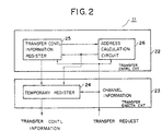
CPU 10 is processing data while exclusively using thesystem bus 15. When a request for the data transfer associated with channel CH0 occurs in the I/O port 12, a request signal REQ0 is supplied to the DMAC 11. Then the DMAC 11 supplies theCPU 10 with a hold request signal HOLD to release thesystem bus 15 from the exclusive use by theCPU 10. When receiving the hold request signal HOLD, theCPU 10 sends a hold acknowledge signal HOLD ACK to the DMAC 11, and then transfers the bus using right to the DMAC 11. Thereby, the DMAC 11 can exclusively use thesystem bus 15, and is allowed to carry out the DMA transfer. Then the DMAC 11 sends a request acknowledge signal ACK0 to the I/O port 12. - FIG.2 is a block diagram of the DMAC 11 illustrating the principle of the present invention. The DMAC 11 includes a
transfer control circuit 22 and atransfer execution circuit 23. Thetransfer execution circuit 23 includes atemporary register 24 used for temporarily storing transfer control information dependent on the transfer request supplied from the device such as the I/O ports 12 and 13, and thememory 14. When the transfer request occurs, based on information including channel information, the corresponding transfer control information stored in thetemporary register 24 is read out by thetransfer execution circuit 23 and is then output to the system bus 15 (FIG.1). The actual data transfer is carried out. During this operation, thetransfer control circuit 22 generates transfer control information related to the next transfer request, and sets the generated transfer control information in thetemporary register 24. The generation for the next transfer request is based on the present transfer control information. Therefore, thetransfer control circuit 22 includes a transfer control information register 25 in which the transfer control information necessary for the DMA transfer is registered before this data transfer is executed. Based on the transfer control information registered in thetransfer register 25, thetransfer control circuit 22 generates transfer control information necessary for processing the next transfer request. - During a time when data is transferred, an
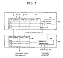
address generation circuit 26 provided in thetransfer control circuit 22 generates, based on the present transfer control information registered in the transfer control information register 25, an address information necessary for processing the next transfer request. The address information is a part of the transfer control information, and generally includes the source and destination addresses. The generated address information necessary for processing the next transfer request is written into the transfer control information register 25 and thetemporary register 24. Thereby, the contents of the transfer control information register 25 are renewed with the generated address information, which is also set in thetemporary register 24. Therefore, when the next transfer request occurs, the transfer control information which is already registered in thetemporary register 24, is immediately read out therefrom, so that the data transfer can be actually made immediately after the transfer request occurs. That is, by beforehand generating the transfer control information necessary for executing the next data transfer and then registering the same in thetemporary register 24 during the present data transfer, it becomes possible to immediately output the transfer control information in response to the transfer request and then start the DMA transfer. Thereby, the processing speed can be extremely increased. - FIG.3 shows an example of the structure for the DMAC 11 illustrated in FIG.2. In FIG.3, those parts that are the same as those in FIG.2 are given the same reference numerals. The DMAC 11 which includes the
transfer control circuit 22 and thetransfer execution circuit 23, has four channels CH0 through CH3. With respect to the request of the DMA transfer supplied from each of the four channels CH0 through CH3, the DMAC 11 is capable of carrying out the DMA transfer in synchronism with a clock signal (not shown). - The transfer control information register 25 in the
transfer control circuit 22 temporarily holds an address (consisting of source and destination addresses), a byte count and control information for each of the channels CH0 to CH3, and is subjected to the writing operation by theCPU 10 or the like prior to the start of the data transfer, for example. The information registered in the transfer control information register 25 is the transfer control information. It is noted that "control information" is a part of the transfer control information. Thetransfer control circuit 22 includes an arithmetic and logic unit (hereafter simply referred to as ALU) 27, and acontrol circuit 28. TheALU 27 generates the address and the byte count for the next transfer request on the basis of information of the address and the byte count registered in the transfercontrol information register 25. This generation can be done for each of the channels CH0 through CH3. Based on the transfer request supplied from a device, thecontrol circuit 28 makes a decision on what transfer control information is necessary for processing the next transfer request, and read outs the necessary transfer control information relating to the requested channel from the transfercontrol information register 25. As will be described in detail later, out of the read-out transfer control information, the control information is supplied to thecontrol circuit 28, which renews the control information necessary for processing the next transfer request, and then registers the renewed control information into thetemporary register 24. - The
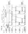
control circuit 28 instructs theALU 27 to generate the address and the byte count necessary for processing the next data transfer by using the address and the byte count registered in the transfercontrol information register 25. The generated results are registered in the transfer control information register 25 and also thetemporary register 24. In this way, thetemporary register 24 holds the transfer control information necessary for executing the next data transfer. The transfer control information registered in thetemporary register 24 is read out by an instruction supplied from atransfer management circuit 29 provided in thetransfer execution circuit 23. Thetransfer management circuit 29 determines the execution channel used in the DMA transfer dependent on the transfer request. Then thetransfer management circuit 29 informs thetransfer control circuit 22 that the data transfer is to be carried out through the determined execution channel, and has thetemporary register 24 output the transfer control information relating to the determined channel to thesystem bus 15. At this time, the DMAC 11 starts the DMA transfer in conformity with the transfer request. As will be described in detail later, thetransfer control circuit 22 and thetransfer execution circuit 23 are mutually coupled through an internal bus (not shown in FIG.3), through which various information is transmitted and received therebetween. - A description is given of operation of the DMAC 11 of FIG.3 with reference to FIG.4, which is a timing chart illustrating the operation of the DMAC 11. A note is given as follows. As shown, the transfer control information is output in a three-clock cycle. The transfer control information which is output from the DMAC 11, is prepared when the previous transfer request occurs and when the present transfer request occurs, the transfer control information necessary for the data transfer of the next transfer request is prepared. Therefore, a description is given on the premise that when the present transfer request occurs, the transfer control information necessary for processing the present transfer request has already been prepared.
- When the transfer request occurs in a channel, the present channel in the DMAC 11 is switched to the requested channel in synchronism with the fall of a clock signal CLK occurring at this time. Then, the transfer control information relating to the requested channel is output to the
system bus 15 from thetemporary register 24 by the control of thetransfer management circuit 29. Thereby, the DMA transfer related to the request channel starts. It is to be noted that the channel switching in the DMAC 11 is made at almost the same time as the transfer request occurs. As a result, there is less delay taken to switch the channel. It is to be noted that a long time must be taken to switch the channel in the conventional DMAC. - At the time of channel switching, the
transfer control circuit 22 is informed of the channel for which the transfer request occurs, under the control of thetransfer management circuit 29. Then, thetransfer management circuit 29 reads out the corresponding transfer control information from thetemporary register 24, and outputs the same to thesystem bus 15. On the other hand, thecontrol circuit 28 generates control information necessary for the next data transfer, and writes the same into the transfer control information register 25 and thetemporary register 24. Thereby, the contents of the control information register 25 are renewed, and at the same time, the contents of thetemporary register 24 are renewed. - Then, the
ALU 27 starts generating (calculating) the address value and the byte count relating to the requested channel for the next data transfer under the control of thecontrol circuit 28. In this address calculation, the generated control information is referred to. Then the generated information is registered, through the internal bus, in the area of thetemporary register 24 relating to said channel. Thereby, the contents of thetemporary register 24 are renewed with the generated address value. At the same time, the address value and the byte count in the transfer control information register 25 relating to the requested channel are replaced with the generated address value and byte count. In this manner, the transfer control information necessary for processing the next transfer request is registered in thetemporary register 24, and is immediately output to thesystem bus 15 when the above next transfer request occurs. It is noted that thetransfer execution circuit 23 itself does not necessitate the byte count, and therefore the byte count is not registered in thetemporary register 24. - For example, when the next transfer request occurs in the fourth clock (4), the transfer control information necessary for this next transfer request is already registered in the
temporary register 24, and is therefore immediately output to thesystem bus 15. By this operation, it is possible to extremely reduce the response time from the transfer request to the start of the data transfer. At this time, the execution channel used for the next data transfer is determined, and the transfer control information necessary for processing the next transfer request through the determined execution channel is registered in thetemporary register 24 ahead of the occurrence of the next transfer request in the same way as the aforementioned operation. - A further description is given of the DMAC 11 shown in FIG.3.
- FIG.5 is a block diagram of the detailed structure of the DMAC 11 of FIG.3. In FIG.5, those parts which are the same as those in FIG.3 are given the same reference numerals. The
control circuit 28 shown in FIG.3 corresponds to a microsequencer 28a and a programmable logic array (hereafter simply referred to as a PLA) 28b. TheALU 27 corresponds to anaddress ALU 27a and acount ALU 27b. Thetransfer control circuit 22 is made up of the transfer control information register 25, the microsequencer 28a, thePLA 28b, theaddress ALU 27a, and thecount ALU 27b. - The transfer control information register 25 includes, for each of the channels CH0 - CH3, a control register (CNTR), a source address register (SAR), a destination address register (DAR), and a byte count register (BCR). The aforementioned transfer control information is made up of control signals registered in the control register CNTR, a source address registered in the source address register SAR, a destination address register DAR, and a byte count registered in the byte count register BCR. In the following description, labels such as CNTR, SAR, DAR and BCR are also used for representing the contents of the corresponding registers. The control register CNTR may be constituted by a state counter used for state indication. The
PLA 28b renews the control information by using the contents of the state counter. The state indication is represented by control signals TC, HDC and NEXTS. That is, the control information to be registered in the control register CNTR includes the control signals TC, HDC and NEXTS. The control signal TC keeps the count of the number of transfers of unit data in three bits, for example, and makes thePLA 28b operate like the microsequencer 28a. The control signal HDC keeps the count of the number of data stored in atemporary data register 32. The control signal NEXTS indicates whether the transfer will next be carried out by a source device or a destination device. The source address SAR is an address of a source device, from which data to be transferred is read out. The destination address indicates an address of a destination device, from which transferred data is written into the device. The byte count BCR indicates the number of bytes of data to be transferred. A signal ID supplied to thePLA 28b from the microsequencer 28a indicates a process mode in two bits so that "00" indicates a normal transfer, "01" indicates an initialization, "10" indicates a chain mode and "11" indicates an exception processing. The microsequencer 28a and thePLA 28b is activated by a signal TREQ, which is generated by the request handler 29a when the transfer request is applied thereto. A signal TACK is supplied to the request handler 29a from thePLA 28b, and allows the request handler 29a to accept the next transfer request. - The
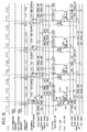
transfer execution circuit 23 is made up of ablock 23a including a request handler 29a, ablock 23b which includes thetemporary register 24, adata swapper 31 and the temporary data register 32, and a function provided by the combination of the microsequencer 28a and thePLA 28b. Thetemporary register 24 is made up of, for each of the channels CH0 - CH3, a control register CNTR', a source address register SAR' and a destination address register DAR'. The control information to be registered in the control register CNTR' includes control signals G, BC and NEXTS. The control signal G is supplied from thePLA 28b, and is used when control rearranging the data in thedata swapper 31. The rearranging of the data includes assembling, disassembling and the like. The data swapper 31 is controlled by the control signal G together with the control signal BC. The control signal BC indicates which portion of the data bus included in thesystem bus 15 should be used. This is suitable for the case where the data bus is a 4-byte data bus, and data to be transferred which is stored in the datatemporary register 32 consists of 4 bytes. - A description is given of operation of the structure of FIG.5. In FIG.6, "TRAN INF" shown with respect to symbol "CONT" indicates control information, and "TRAN INF" shown with respect to symbol "ADDS" indicates address and byte count.
- It is now assumed that as shown in FIG.6, the CH0 transfer request and CH1 transfer request occur at the same time. It is also assumed that the channels CH0 and CH1 are alternately used for the DMA transfer. It is further assumed that both the priorities are identical to each other, and the CH0 transfer request is first accepted by the request handler 29a (FIG.5). Then, the execution channel is immediately switched to the channel CH0. In response to the CH0 transfer request, as indicated by S1 in FIG.6, the microsequencer 28a controls the
PLA 28b so that the transfer control information relating to the channel CH0 registered thetemporary register 24 is read out therefrom. That is, the control information, namely, the control information CNTR' relating to the channel CH0 is read out from the temporary register 24 (S2), and then the source address SAR' or the destination address DAR' relating to the channel CH0 are read out therefrom (S3). It is to be noted that the control counter CNTR', the source and destination addresses SAR' and DAR' are already generated during the DMA transfer just prior to the present CH0 transfer request. - On the other hand, in response to the CH0 transfer request, the microsequencer 28a makes the
PLA 28b renew the control information (CNTR, CNTR') for the next (second) transfer request, or in other words, the next data transfer through the channel CH0. In the renewal of the control information, the control information CNTR relating to the channel CH0 which is presently registered in the transfer control information register 25 (first data transfer) is referred to by thePLA 28b (S5). As described previously, the control information with respect to the transfer control information register 25 includes the control signals TC, HDC and NEXTS shown in FIG.5, and the control information with respect to thetemporary register 24 includes the control signals G and BC. That is, the PLA 28a generates those control signals at the same time. The renewed control information CNTR with respect to thetemporary register 24 is output to the internal data bus 50 (S6), and is then written into the control register CNTR' relating to the channel CH0 in the temporary register 24 (S7). On the other hand, the renewed control information CNTR with respect to the transfer information register 25 is written into the control register CNTR relating to the channel CH0 in the transfer control information register 25 (S8). The operations of S6 and S8 occur at the same time. - On the other hand, the
ALUs PLA 28b so as to generate the source address SAR, the destination address DSR and the byte count BCR which are related to the next (second) data transfer through the channel CH0 (S9). This occurs at almost the same time as the operations of S6 and S8. In this generation, the source address SAR, the destination address DSR and the byte count BCR relating to the present (first) data transfer through the channel CH0 are referred to (S10). Then, the generated source address SAR and destination address DAR are output to the internal data bus 50 (S11), and are then written into the corresponding registers SAR' and DAR' relating to the channel CH0 in the temporary register 24 (S12). On the other hand, the generated source address SAR, destination address DAR and byte count BCR are written into the corresponding registers in the transfer control information register 25 which relate to the channel CH0 (S13). - In this way, it becomes possible to immediately read out the control information CNTR', the start address SAR' and the destination address DAR' from the
temporary register 24, when the next (second) transfer request through the channel CH0 occurs in response to the channel switching made in synchronism with the fall of the clock CLK. At the same time, the transfer control information for the next data transfer is generated. - The above-mentioned operation with respect to the channel CH0 holds true for the operation with respect to the channel CH1 shown in FIG.6. Therefore, a corresponding operation is omitted.
- The present invention is not limited to the aforementioned embodiments, and variations and modifications may be made without departing from the scope of the invention.
Claims (11)
- A direct memory access controller coupled to a system bus (15) of a system for controlling data transfers through a plurality of channels by a direct memory access, comprising request handling means (29a) for receiving a transfer request generated by a device connected to said system bus, and first register means (25) for storing transfer control information used for obtaining transfer control information necessary for executing the data transfer by a next transfer request supplied from said request handling means, characterized in that said direct memory access controller comprises second register means (24) for storing said transfer control information necessary for processing the next transfer request, transfer control information setting means (27a, 27b, 28a, 28b) for generating said transfer control information necessary for processing the next transfer request on the basis of the transfer control information registered in said first register means (25) during the data transfer by the present transfer request and then renewing said first and second register means (25, 24) with the generated transfer control information; and transfer execution means (31, 32) for executing the actual data transfer through said system bus (15) in accordance with the transfer control information registered in the second register means (24), which is output to said system bus therefrom.
- A direct memory access controller as claimed in claim 1, characterized in that each of said first and second register means (25, 24) comprises a register portion assigned to each of said plurality of channels.
- A direct memory access controller as claimed in any of claims 1 and 2, characterized in that said transfer control information setting means (27a, 27b, 28a, 28b) starts to generate the transfer control information necessary for processing the next transfer request when the present transfer request occurs.
- A direct memory access controller as claimed in any of claims 1 to 3, characterized in that said first register means (25) comprises, for each of said channels, a first register (CNTR) which registers a control information necessary for controlling the data transfer, a second register (BCR) which registers a byte count indicative of a amount of data to be transferred, and a third register (SAR, DAR) which registers address information relating to the data transfer, and that said control information, said byte count and said address information form said transfer control information to be registered in the first register means.
- A direct memory access controller as claimed in any of claims 1 to 4, characterized in that said second register means (24) comprises, for each of said channels, a first register (CNTR') which registers a control information necessary for controlling the data transfer by said next transfer request, and a second register (SAR', DAR') for registering address information relating to the data transfer by said next transfer request, and that said control information and said address information form the transfer control information to be registered in said second register means.
- A direct memory access controller as claimed in any of claims 1 to 5, characterized in that said transfer control information setting means (27a, 27b, 28a, 28b) comprises a programmable logic array (28b) for controlling a sequence of the data transfer executed by said transfer execution means (31, 32) and a sequence of generating said transfer control information, a microsequencer (28a) for controlling said programmable logic array (28b), and an arithmetic and logic unit (27a, 27b) for generating said transfer control information necessary for processing the next transfer request.
- A direct memory access controller as claimed in claim 6, characterized in that said transfer control information includes a control information (CNTR) necessary for controlling the data transfer, a byte count (BCR) indicative of an amount of data to be transferred, and an address information including a source address (SAR) and a destination address (DAR) relating to the data transfer.
- A direct memory access controller as claimed in any of claims 1 to 7, characterized by further comprising an internal bus (50) to which said first and second register means (25, 24) are coupled.
- A direct memory access controller as claimed in any of claims 1 to 8, characterized in that said second register means (24) is coupled to said system bus (15).
- A direct memory access controller as claimed in claim 6, characterized in that said arithmetic and logic unit comprises a first arithmetic and logic unit (27a) for generating the source and destination addresses (SAR, DAR) and a second arithmetic and logic unit (27b) for generating the byte count (BCR).
- A direct memory access controller as claimed in any of claims 1 to 10, characterized in that said transfer execution means comprises a data temporary register (32) for temporary storage of data to be transferred, and a data swapper (31) which controls an exchange of data between said system bus (15) and said data temporary register (32).
Applications Claiming Priority (2)
| Application Number | Priority Date | Filing Date | Title |
|---|---|---|---|
| JP66137/88 | 1988-03-18 | ||
| JP63066137A JPH01237864A (en) | 1988-03-18 | 1988-03-18 | Dma transfer controller |
Publications (3)
| Publication Number | Publication Date |
|---|---|
| EP0333594A2 EP0333594A2 (en) | 1989-09-20 |
| EP0333594A3 EP0333594A3 (en) | 1991-10-23 |
| EP0333594B1 true EP0333594B1 (en) | 1997-08-13 |
Family
ID=13307174
Family Applications (1)
| Application Number | Title | Priority Date | Filing Date |
|---|---|---|---|
| EP89400746A Expired - Lifetime EP0333594B1 (en) | 1988-03-18 | 1989-03-16 | Direct memory access controller |
Country Status (4)
| Country | Link |
|---|---|
| US (1) | US5438665A (en) |
| EP (1) | EP0333594B1 (en) |
| JP (1) | JPH01237864A (en) |
| KR (1) | KR920007905B1 (en) |
Families Citing this family (34)
| Publication number | Priority date | Publication date | Assignee | Title |
|---|---|---|---|---|
| EP0378422B1 (en) * | 1989-01-13 | 1995-07-26 | International Business Machines Corporation | Look ahead bus transfer request |
| JPH03156554A (en) * | 1989-11-14 | 1991-07-04 | Hitachi Ltd | Data transfer control system |
| DE69128565T2 (en) * | 1990-06-25 | 1998-06-04 | Nec Corp | Microcomputer equipped with a DMA controller |
| US5182800A (en) * | 1990-11-16 | 1993-01-26 | International Business Machines Corporation | Direct memory access controller with adaptive pipelining and bus control features |
| US5287476A (en) * | 1991-06-07 | 1994-02-15 | International Business Machines Corp. | Personal computer system with storage controller controlling data transfer |
| JP2599539B2 (en) * | 1991-10-15 | 1997-04-09 | インターナショナル・ビジネス・マシーンズ・コーポレイション | Direct memory access device and look-ahead device |
| US5721954A (en) * | 1992-04-13 | 1998-02-24 | At&T Global Information Solutions Company | Intelligent SCSI-2/DMA processor |
| US5513368A (en) * | 1993-07-16 | 1996-04-30 | International Business Machines Corporation | Computer I/O adapters for programmably varying states of peripheral devices without interfering with central processor operations |
| US5644787A (en) * | 1993-08-03 | 1997-07-01 | Seiko Epson Corporation | Apparatus for controlling data transfer between external interfaces through buffer memory using table data having transfer start address transfer count and unit selection parameter |
| JP3647055B2 (en) * | 1993-11-17 | 2005-05-11 | キヤノン株式会社 | Information processing system, management method, and management apparatus |
| US5628026A (en) * | 1994-12-05 | 1997-05-06 | Motorola, Inc. | Multi-dimensional data transfer in a data processing system and method therefor |
| DE69610450T2 (en) * | 1995-03-13 | 2001-04-26 | Sun Microsystems Inc | Virtual input / output processor |
| EP0732659B1 (en) * | 1995-03-17 | 2001-08-08 | LSI Logic Corporation | Controlling (n+i) I/O channels with (n) data managers in a homogeneous software programming environment |
| US5864712A (en) * | 1995-03-17 | 1999-01-26 | Lsi Logic Corporation | Method and apparatus for controlling (N+I) I/O channels with (N) data managers in a homogenous software programmable environment |
| SE515737C2 (en) * | 1995-03-22 | 2001-10-01 | Ericsson Telefon Ab L M | Apparatus and method for handling digital signals and a processing device comprising such |
| US5826106A (en) * | 1995-05-26 | 1998-10-20 | National Semiconductor Corporation | High performance multifunction direct memory access (DMA) controller |
| US5713044A (en) * | 1995-12-19 | 1998-01-27 | Intel Corporation | System for creating new group of chain descriptors by updating link value of last descriptor of group and rereading link value of the updating descriptor |
| US5870627A (en) * | 1995-12-20 | 1999-02-09 | Cirrus Logic, Inc. | System for managing direct memory access transfer in a multi-channel system using circular descriptor queue, descriptor FIFO, and receive status queue |
| US6381293B1 (en) * | 1996-04-03 | 2002-04-30 | United Microelectronics Corp. | Apparatus and method for serial data communication between plurality of chips in a chip set |
| US5963609A (en) * | 1996-04-03 | 1999-10-05 | United Microelectronics Corp. | Apparatus and method for serial data communication between plurality of chips in a chip set |
| DE69735614T2 (en) * | 1996-10-18 | 2006-09-07 | Matsushita Electric Industrial Co., Ltd., Kadoma | Data transmission device and data transmission system for arbitrating multiple I / O ports in DMA |
| US5924110A (en) * | 1996-12-06 | 1999-07-13 | Ncr Corporation | Multischeme memory management system for computer |
| US5978866A (en) * | 1997-03-10 | 1999-11-02 | Integrated Technology Express, Inc. | Distributed pre-fetch buffer for multiple DMA channel device |
| US6006293A (en) * | 1998-04-21 | 1999-12-21 | Comsat Corporation | Method and apparatus for zero overhead sharing for registered digital hardware |
| JP2000151641A (en) * | 1998-11-13 | 2000-05-30 | Sony Corp | Transmission control method and transmitter |
| JP2000315186A (en) * | 1999-05-06 | 2000-11-14 | Hitachi Ltd | Semiconductor device |
| US7457896B1 (en) * | 1999-08-25 | 2008-11-25 | Seagate Technology Llc | Automated register data transfer to reduce processing burden on a processing device |
| US6782465B1 (en) | 1999-10-20 | 2004-08-24 | Infineon Technologies North America Corporation | Linked list DMA descriptor architecture |
| US6499077B1 (en) * | 1999-12-30 | 2002-12-24 | Intel Corporation | Bus interface unit for reflecting state information for a transfer request to a requesting device |
| US20040093439A1 (en) * | 2002-09-24 | 2004-05-13 | Rohm Co., Ltd | Data processing control apparatus and DMA controller |
| WO2005059757A1 (en) * | 2003-12-19 | 2005-06-30 | Matsushita Electric Industrial Co.,Ltd. | Recording device control apparatus |
| DE102004006767B4 (en) * | 2004-02-11 | 2011-06-30 | Infineon Technologies AG, 81669 | Method and device for transporting data sections by means of a DMA controller |
| JP5287301B2 (en) * | 2009-01-30 | 2013-09-11 | 富士通株式会社 | Descriptor transfer device, I / O controller, and descriptor transfer method |
| CN104123252A (en) * | 2013-04-26 | 2014-10-29 | 韩国科亚电子股份有限公司 | Multi-channel direct memory access controller and control method thereof |
Family Cites Families (24)
| Publication number | Priority date | Publication date | Assignee | Title |
|---|---|---|---|---|
| JPS5584858A (en) * | 1978-12-18 | 1980-06-26 | Nippon Denso Co Ltd | Engine control |
| US4354225A (en) * | 1979-10-11 | 1982-10-12 | Nanodata Computer Corporation | Intelligent main store for data processing systems |
| JPS5660933A (en) * | 1979-10-22 | 1981-05-26 | Nec Corp | Information processor |
| US4387433A (en) * | 1980-12-24 | 1983-06-07 | International Business Machines Corporation | High speed data interface buffer for digitally controlled electron beam exposure system |
| US4481578A (en) * | 1982-05-21 | 1984-11-06 | Pitney Bowes Inc. | Direct memory access data transfer system for use with plural processors |
| DE3241376A1 (en) * | 1982-11-09 | 1984-05-10 | Siemens AG, 1000 Berlin und 8000 München | DMA CONTROL DEVICE FOR TRANSMITTING DATA BETWEEN A DATA TRANSMITTER AND A DATA RECEIVER |
| US4713750A (en) * | 1983-03-31 | 1987-12-15 | Fairchild Camera & Instrument Corporation | Microprocessor with compact mapped programmable logic array |
| US4530053A (en) * | 1983-04-14 | 1985-07-16 | International Business Machines Corporation | DMA multimode transfer controls |
| US4665482A (en) * | 1983-06-13 | 1987-05-12 | Honeywell Information Systems Inc. | Data multiplex control facility |
| JPS6057457A (en) * | 1983-09-07 | 1985-04-03 | Ricoh Co Ltd | Dma device |
| US4805097A (en) * | 1984-08-03 | 1989-02-14 | Motorola Computer Systems, Inc. | Memory management unit with dynamic page allocation |
| JPH0760423B2 (en) * | 1984-12-24 | 1995-06-28 | 株式会社日立製作所 | Data transfer method |
| JPS61198351A (en) * | 1985-02-28 | 1986-09-02 | Toshiba Corp | Direct memory access control circuit |
| US4797812A (en) * | 1985-06-19 | 1989-01-10 | Kabushiki Kaisha Toshiba | System for continuous DMA transfer of virtually addressed data blocks |
| US4847750A (en) * | 1986-02-13 | 1989-07-11 | Intelligent Instrumentation, Inc. | Peripheral DMA controller for data acquisition system |
| US4821185A (en) * | 1986-05-19 | 1989-04-11 | American Telephone And Telegraph Company | I/O interface system using plural buffers sized smaller than non-overlapping contiguous computer memory portions dedicated to each buffer |
| JPS6329868A (en) * | 1986-07-23 | 1988-02-08 | Nec Corp | Dma controller |
| US5093910A (en) * | 1986-10-29 | 1992-03-03 | United Technologies Corporation | Serial data transmission between redundant channels |
| US4782439A (en) * | 1987-02-17 | 1988-11-01 | Intel Corporation | Direct memory access system for microcontroller |
| JPS63262745A (en) * | 1987-04-20 | 1988-10-31 | Yokogawa Electric Corp | Address forming circuit |
| EP0288649B1 (en) * | 1987-04-22 | 1992-10-21 | International Business Machines Corporation | Memory control subsystem |
| US5018098A (en) * | 1987-05-07 | 1991-05-21 | Fujitsu Limited | Data transfer controlling apparatus for direct memory access |
| DE68927015D1 (en) * | 1988-02-08 | 1996-10-02 | Fujitsu Ltd | Direct memory access control |
| JPH0831079B2 (en) * | 1988-02-08 | 1996-03-27 | 富士通株式会社 | DMA controller |
-
1988
- 1988-03-18 JP JP63066137A patent/JPH01237864A/en active Pending
-
1989
- 1989-03-16 EP EP89400746A patent/EP0333594B1/en not_active Expired - Lifetime
- 1989-03-17 KR KR1019890003350A patent/KR920007905B1/en not_active IP Right Cessation
-
1994
- 1994-02-01 US US08/194,871 patent/US5438665A/en not_active Expired - Lifetime
Non-Patent Citations (3)
| Title |
|---|
| 1537, New York, US; "Multi-microprocessor data delivery system" * |
| Patent Abstracts of Japan, vol. 12 no.238 (P-726) 7 July 1988 & JP63-29868 NEC Corp. 8 February 1988 * |
| Patent Abstracts of Japan, vol. 5 no.118 (P-073) 30 July 1981 & JP56-060933 NEC Corp. 26 May 1981 * |
Also Published As
| Publication number | Publication date |
|---|---|
| EP0333594A3 (en) | 1991-10-23 |
| JPH01237864A (en) | 1989-09-22 |
| KR890015143A (en) | 1989-10-28 |
| EP0333594A2 (en) | 1989-09-20 |
| KR920007905B1 (en) | 1992-09-19 |
| US5438665A (en) | 1995-08-01 |
Similar Documents
| Publication | Publication Date | Title |
|---|---|---|
| EP0333594B1 (en) | Direct memory access controller | |
| JP2829091B2 (en) | Data processing system | |
| US4467447A (en) | Information transferring apparatus | |
| EP0141742A2 (en) | Buffer system for input/output portion of digital data processing system | |
| EP0172038B1 (en) | Information processor | |
| US5287471A (en) | Data transfer controller using direct memory access method | |
| JPH0760423B2 (en) | Data transfer method | |
| US5077664A (en) | Direct memory access controller | |
| EP0328450B1 (en) | Direct memory access controller | |
| EP0338564B1 (en) | Microprogram branching method and microsequencer employing the method | |
| EP0331487B1 (en) | Data transfer control system | |
| US4665481A (en) | Speeding up the response time of the direct multiplex control transfer facility | |
| EP0560393B1 (en) | Microprocessor and data processing system with register file | |
| EP0410382A2 (en) | Data transfer controller using direct memory access method | |
| JPH0736806A (en) | Dma system | |
| JP2707256B2 (en) | Micro computer | |
| JP2710219B2 (en) | DMA controller | |
| JP2581144B2 (en) | Bus control device | |
| JPH10334038A (en) | Data transfer device | |
| JPH06274450A (en) | Data transfer system | |
| JPS58189719A (en) | Data transfer control system | |
| JPH01201759A (en) | Dma controller | |
| JPH04109351A (en) | Dma controller | |
| JPH07146839A (en) | Dma circuit | |
| EP0280523A2 (en) | Computer system conversion apparatus |
Legal Events
| Date | Code | Title | Description |
|---|---|---|---|
| PUAI | Public reference made under article 153(3) epc to a published international application that has entered the european phase |
Free format text: ORIGINAL CODE: 0009012 |
|
| AK | Designated contracting states |
Kind code of ref document: A2 Designated state(s): DE FR GB |
|
| PUAL | Search report despatched |
Free format text: ORIGINAL CODE: 0009013 |
|
| AK | Designated contracting states |
Kind code of ref document: A3 Designated state(s): DE FR GB |
|
| 17P | Request for examination filed |
Effective date: 19920305 |
|
| RAP1 | Party data changed (applicant data changed or rights of an application transferred) |
Owner name: FUJITSU LIMITED Owner name: FUJITSU DEVICES INC |
|
| 17Q | First examination report despatched |
Effective date: 19950203 |
|
| GRAG | Despatch of communication of intention to grant |
Free format text: ORIGINAL CODE: EPIDOS AGRA |
|
| GRAH | Despatch of communication of intention to grant a patent |
Free format text: ORIGINAL CODE: EPIDOS IGRA |
|
| RBV | Designated contracting states (corrected) |
Designated state(s): FR |
|
| GRAH | Despatch of communication of intention to grant a patent |
Free format text: ORIGINAL CODE: EPIDOS IGRA |
|
| REG | Reference to a national code |
Ref country code: DE Ref legal event code: 8566 |
|
| GRAA | (expected) grant |
Free format text: ORIGINAL CODE: 0009210 |
|
| AK | Designated contracting states |
Kind code of ref document: B1 Designated state(s): FR |
|
| ET | Fr: translation filed | ||
| PLBE | No opposition filed within time limit |
Free format text: ORIGINAL CODE: 0009261 |
|
| STAA | Information on the status of an ep patent application or granted ep patent |
Free format text: STATUS: NO OPPOSITION FILED WITHIN TIME LIMIT |
|
| 26N | No opposition filed | ||
| PGFP | Annual fee paid to national office [announced via postgrant information from national office to epo] |
Ref country code: FR Payment date: 20070308 Year of fee payment: 19 |
|
| REG | Reference to a national code |
Ref country code: FR Ref legal event code: ST Effective date: 20081125 |
|
| PG25 | Lapsed in a contracting state [announced via postgrant information from national office to epo] |
Ref country code: FR Free format text: LAPSE BECAUSE OF NON-PAYMENT OF DUE FEES Effective date: 20080331 |