EP0314197A2 - A four level frequency shift keying optical communication apparatus - Google Patents
A four level frequency shift keying optical communication apparatus Download PDFInfo
- Publication number
- EP0314197A2 EP0314197A2 EP88118161A EP88118161A EP0314197A2 EP 0314197 A2 EP0314197 A2 EP 0314197A2 EP 88118161 A EP88118161 A EP 88118161A EP 88118161 A EP88118161 A EP 88118161A EP 0314197 A2 EP0314197 A2 EP 0314197A2
- Authority
- EP
- European Patent Office
- Prior art keywords
- signal
- delay
- communication apparatus
- optical communication
- phase shift
- Prior art date
- Legal status (The legal status is an assumption and is not a legal conclusion. Google has not performed a legal analysis and makes no representation as to the accuracy of the status listed.)
- Granted
Links
Images

Classifications
-
- H—ELECTRICITY
- H04—ELECTRIC COMMUNICATION TECHNIQUE
- H04B—TRANSMISSION
- H04B10/00—Transmission systems employing electromagnetic waves other than radio-waves, e.g. infrared, visible or ultraviolet light, or employing corpuscular radiation, e.g. quantum communication
- H04B10/60—Receivers
-
- H—ELECTRICITY
- H04—ELECTRIC COMMUNICATION TECHNIQUE
- H04L—TRANSMISSION OF DIGITAL INFORMATION, e.g. TELEGRAPHIC COMMUNICATION
- H04L27/00—Modulated-carrier systems
- H04L27/10—Frequency-modulated carrier systems, i.e. using frequency-shift keying
- H04L27/14—Demodulator circuits; Receiver circuits
Definitions
- the invention relates to a four level Frequency Shift Keying (called “FSK” hereinafter) optical communication apparatus, and more particularly to a four level FSK optical communication apparatus in which frequency of light is modulated in accordance with informations by four levels.
- FSK Frequency Shift Keying
- a semiconductor laser in which oscillation is performed with the single axis mode and the high spectrum purity can be utilized because the characteristic of the semiconductor laser is improved. Therefore, a coherent optical communication system in which frequency and phase of light are used for transmitting informations can be realized with the high sensitivity.
- a FSK modulation system in which frequency of light is varied dependent on informations especially, long distance transmission can be realized without any repeater because the insertion loss of an external modulator is avoided for the reason why modulated light is easily obtained in accordance with the direct modulation of light in which signal current of low levels is added to bias current of the semiconductor laser.
- transmitting signals are reproduced in accordance with the demodulation of phase informations based on frequency informations by use of a delay detection circuit etc.
- the frequency deviation can be decreased down to a half of transmission rate which is the minimum frequency deviation necessary for the independency of signals. Therefore, the modulation spectrum band can be narrowered.
- a binary continuous phase FSK system which is suitable for a high speed modulation system as reported in "The experiment of 2Gb/s optical heterodyne transmission" described in "the Technical Digest of the Institute of Electronics, Information and Communication Engineers, 1987, 70 year Anniversary National Convention Record, part 10, 2369.”
- a multiple level code communication system is an advantageous system by which a large capacity of data are transmitted in a communication system having a limited transmission capacity due to response speed of devices included therein.
- informations can be transmitted in capacity as much as twice in the same modulation rate in a case where, for instance, two binary codes are converted into a four level code. For this reason, the transmission capacity becomes twice by using a device of a response speed which is the same as that required in a binary code transmission.
- a four level FSK optical communication apparatus comprises a light source for emitting signal light.
- the signal light is modulated in FSK with four level transmitting signal.
- the FSK modulated signal light is combined in an optical coupler with local oscillation light supplied from a local oscillation light source, and combined signal light and local oscillation light are converted to intermediate frequency electric signal at an opto-electric conversion cirsuit.
- the electric signal is divided into two divided signal, one of which is delayed in a delay circuit.
- the delayed signal and the remaining one of the two divided signals are mixed in a first multiplier to produce first detection signal.
- signal selected from the delayed signal and the remaining one of the two divided signals is delayed in a phase shift circuit by ⁇ /2.
- signal having the phase shift of ⁇ /2 and signal having no phase shift are mixed in a second multiplier to produce second detection signal.
- FSK modulation signal is demodulated.
- Fig. 1 there is shown a four level FSK optical communication apparatus in the first embodiment according to the invention.
- the four level FSK communication apparatus is applied to a continuous phase FSK modulation system in which the transmission capacity is 2 x 2 Gb/s, and the modulation index is 0.25, that is, intermediate frequencies f1, f2, f3 and f4 of four levels are set to be 2.25GHz, 2.75GHz, 3.25 GHz and 3.75GHz.
- the four level FSK communication apparatus comprises a signal light source 1 of an external resonator type semiconductor laser which is directly modulated to emit signal light 3 by four level transmitting signal 2, an optical fiber 4 through which the signal light 3 is transmitted, a local oscillation light source 5 of an external resonator type semiconductor laser for emitting local oscillation light 5, a coupler 7 for combining the signal light 3 and the local oscillation light 6 to produce combined light, a balanced receiver 8 for converting the combined light into electric signal, an amplifier 9 for amplifying the electric signal, a band-pass filter 10 having low and high cut-off frequencies of 2GHz and 4GHz, first and second delay detection circuits 11 and 12 for discriminating frequency of signal passed through the band-pass filter 10, and discrimination circuits 13 and 14 in which signals of channels 1 and 2 are discriminated.
- the first and second delay detection circuits 11 and 12 comprise a delay line 15 for applying a predetermined delay time to one of divided signals supplied from the band-pass filter 10, a 90° hybrid divider 16 for dividing signal propagated through the delay line 15 into two signals, and mixers 17 and 18 for mixing non-delayed signals and the two signals supplied from the 90° hybrid divider 16 correspondingly as shown in Fig. 1.
- the light source 1 of the semiconductor laser is directly modulated to emit the signal light 3 by the four level transmitting signal 2, so that the frequency of the signal light 3 is modulated with four levels of continuous phase having the frequency separation of 0.5GHz.
- the signal light 3 thus modulated is transmitted through the optical fiber 4, and then combined in the coupler 7 with the local oscillation light 6 supplied from the local oscillation light source 5.
- the light thus combined has the beat spectrum width of 1MHz and is received in the balanced receiver 8 to be converted into the electric signal which is then amplified in the amplifier 9.
- the amplified electric signal of a predetermined band is passed through the band-pass filter 10, and then supplied to the delay detection circuits 11 and 12.
- the signal is delayed through the delay line 15 by the predetermined delay time, and divided in the 90° hybrid divider 16 into the two signals having the phase shift of 90°( ⁇ /2).
- the two signals thus divided are supplied to the mixers 17 and 18 in which the two divided signals are mixed with the non delayed signals respectively.
- the frequency discrimination of the signal is performed in the delay detection circuits 11 and 12.
- the signal diserimination of the channels 1 and 2 is performed in the diserimination circuits 11 and 12.
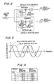
- Fig. 2 shows first and second delay detection circuits 202 and 203 which are used in place of the first and second delay detection circuits 11 and 12 in the first embodiment.
- the first and second delay detection circuits 202 and 203 comprise delay lines 204 and 207, mixers 205 and 208, and low-pass filters 209 and 210, respectively.
- the second delay detection circuit 203 further comprises a ⁇ /2 phase shifter 206 inserted parallel to the delay line 207.
- Fig. 3 shows the characteristics of the first and second delay detection circuits 202 and 203 having the phase shift difference of ⁇ /2. If it is assumed that the four frequency levels are f1, f2, f3 and f4 as shown in Fig. 3, two outputs of the first and second delay detection circuits 202 and 203 are obtained as shown in Fig. 4. Therefore, electric signal 201 supplied to the input of the delay detection circuits 202 and 203 is discriminated as signals of channels 1 and 2 dependent on the positive and negative values and combination of delay detection outputs 211 and 213. Absolute value of the delay detection outputs 211 and 212 is " ⁇ 2/2" less than "1" which is obtained in a continuous phase FSK delay detection system. Therefore, the demodulation efficiency is decreased as compared thereto. If it is compared in regard to the sensitivity, the difference turns to be 3dB. That is, the four level FSK optical communication apparatus is identical to a binary continuous phase FSK delay detection system in terms of the transmissin capacity versus the sensitivity.
- the delay time T is set to be one bit in the first embodiment.
- a four level FSK optical communication apparatus in which the transmission capacity becomes twice as compared to a binary code transmission system without the burden on the response speed of frequency modulation in a light source.
- the intermediate frequency band of the invention is approximately a half of that in the binary continuous phase FSK detection system. This means that the invention is advantageous in realizing a system of a large capacity in accordance with the frequency multiplexing etc.
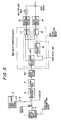
- Fig. 5 there is shown a four level FSK optical communicatin apparatus in the second embodiment according to the invention.
- the four level FSK optical communication apparatus in which like parts are indicated by like reference numerals in the first embodiment except that 501 indicates a band-pass filter, 502 a further provided 90° hybrid divider, 503 a delay line, 504 a newly inserted multiplier, 505 and 506 first and second delay detection circuits, and 507 an adder.
- the light source 1 is composed of a semiconductor laser having the spectrum width of 1MHz and the cut-off frequency of 1GHz in frequency modulation.
- the modulating signal 2 is four level signal having the bit rate of 1Gb/s which is equal to the bit rate of 2Gb/s in a binary system, and the modulation index m is set to be as large as "0.5" which is twice that in the first embodiment for the limited tolerance of the spectrum width.
- the multiplier 504 and the adder 505 binary signals of two channels which are demodulated are again converted to a four level signal.
- respective signal frequencies in the intermediate frequency band are set on the lower frequency side because the base band signal band can be half as compared to that in the first embodiment because of the lowered transmission rate which is half that in the first embodiment.
- the modulating frequencies f1, f2, f3 and f4 are 1.25GHz, 1.75GHz, 2.25GHx and 2.75 GHz, respectively. Consequently, the band for the band-pass filter 501 through which the intermediate frequency signal is passed is adapted thereto, such that the low-band cut-off frequency is 1GHz, and the high-band cut-off frequency is 3GHz.
- a 2 x 1Bb/s four level FSK optical communication repeater system in which the spectrum width tolerance of a light source is moderate and the light source is not heavily burdened in the response speed for frequency modulation can be provided in the second embodiment.
- the receiving sensitivity is -40dBm which is approximately identical to a 2Gb/s binary continuous phase FSK delay detection system.
- a four level FSK optical communication apparatus may be modified, for instance, such that an unity semiconductor laser is possible to be adopted therein because the spectrum width tolerance of a light source can be large if a delay detection circuit is optimized in compliance with the modulation index which is set to be large. Furthermore, the four level FSK optical communication apparatus can be applied to a frequency division multiplexing transmission of high density because the intermediate frequency signal band is narrow.
Landscapes
- Engineering & Computer Science (AREA)
- Computer Networks & Wireless Communication (AREA)
- Signal Processing (AREA)
- Physics & Mathematics (AREA)
- Electromagnetism (AREA)
- Optical Communication System (AREA)
- Digital Transmission Methods That Use Modulated Carrier Waves (AREA)
Abstract
Description
- The invention relates to a four level Frequency Shift Keying (called "FSK" hereinafter) optical communication apparatus, and more particularly to a four level FSK optical communication apparatus in which frequency of light is modulated in accordance with informations by four levels.
- In these days, a semiconductor laser in which oscillation is performed with the single axis mode and the high spectrum purity can be utilized because the characteristic of the semiconductor laser is improved. Therefore, a coherent optical communication system in which frequency and phase of light are used for transmitting informations can be realized with the high sensitivity. In a FSK modulation system in which frequency of light is varied dependent on informations, especially, long distance transmission can be realized without any repeater because the insertion loss of an external modulator is avoided for the reason why modulated light is easily obtained in accordance with the direct modulation of light in which signal current of low levels is added to bias current of the semiconductor laser. In the FSK modulation system, transmitting signals are reproduced in accordance with the demodulation of phase informations based on frequency informations by use of a delay detection circuit etc. in which the continuous phase characteristic of frequency modulated light is utilized because the frequency modulated light obtained from the semiconductor laser directly modulated has the continuous-phase characteristic. According to such a FSK modulation system, a sensitivity which is substantially equal to that of a phase shift keying modulation system having the highest sensitivity among the various kinds of modulation systems.
- In the FSK modulation system, the frequency deviation can be decreased down to a half of transmission rate which is the minimum frequency deviation necessary for the independency of signals. Therefore, the modulation spectrum band can be narrowered. Especially, research and development have been intensively promoted in a binary continuous phase FSK system which is suitable for a high speed modulation system as reported in "The experiment of 2Gb/s optical heterodyne transmission" described in "the Technical Digest of the Institute of Electronics, Information and Communication Engineers, 1987, 70 year Anniversary National Convention Record,
part 10, 2369." - On the other hand, a multiple level code communication system is an advantageous system by which a large capacity of data are transmitted in a communication system having a limited transmission capacity due to response speed of devices included therein. In such a multiple level code communication system, informations can be transmitted in capacity as much as twice in the same modulation rate in a case where, for instance, two binary codes are converted into a four level code. For this reason, the transmission capacity becomes twice by using a device of a response speed which is the same as that required in a binary code transmission.
- According to the binary continuous phase FSK modulation system, however, the possibility of being applied to a detection system in a multiple level continuous phase FSK modulation system has not been studied. Therefore, a semiconductor device must be developed to increase the response speed in frequency modulation in a case where a high speed continuous phase FSK modulation system using a semiconductor laser is required to be put into a practical use.
- Accordingly, it is an object of the invention to provide a four level FSK optical communication apparatus, the sensitivity of which is high to be substantially equal to that of a binary continuous phase FSK delay detection system in the same transmission capacity between the four and binary FSK optical communication apparatus.
- It is a further object of the invention to provide a four level FSK optical communication apparatus in which the response speed of frequency modulation is high without the necessity for the development of a semiconductor device having a high response speed.
- According to the invention, a four level FSK optical communication apparatus comprises a light source for emitting signal light. The signal light is modulated in FSK with four level transmitting signal. The FSK modulated signal light is combined in an optical coupler with local oscillation light supplied from a local oscillation light source, and combined signal light and local oscillation light are converted to intermediate frequency electric signal at an opto-electric conversion cirsuit. The electric signal is divided into two divided signal, one of which is delayed in a delay circuit. The delayed signal and the remaining one of the two divided signals are mixed in a first multiplier to produce first detection signal. Further, signal selected from the delayed signal and the remaining one of the two divided signals is delayed in a phase shift circuit by π/2. Then, signal having the phase shift of π/2 and signal having no phase shift are mixed in a second multiplier to produce second detection signal. Thus, FSK modulation signal is demodulated.
- The invention will be explained in more detail in conjunction with appended drawings wherein,
- Fig. 1 is a block diagram showing a four level FSK optical communication apparatus in a first embodiment according to the invention,
- Fig. 2 is a block diagram showing delay detection circuits used in the invention,
- Fig. 3 is an explanatory diagram showing the characteristics of the delay detection circuits shown in Fig. 2,
- Fig. 4 is an explanatory diagram showing relations between outputs of the delay detection circuits shown in Fig. 2 and modulating frequencies, and
- Fig. 5 is a block diagram showing a four level FSK communication apparatus in a second embodiment according to the invention.
- In Fig. 1, there is shown a four level FSK optical communication apparatus in the first embodiment according to the invention. The four level FSK communication apparatus is applied to a continuous phase FSK modulation system in which the transmission capacity is 2 x 2 Gb/s, and the modulation index is 0.25, that is, intermediate frequencies f₁, f₂, f₃ and f₄ of four levels are set to be 2.25GHz, 2.75GHz, 3.25 GHz and 3.75GHz. The four level FSK communication apparatus comprises a
signal light source 1 of an external resonator type semiconductor laser which is directly modulated to emitsignal light 3 by fourlevel transmitting signal 2, anoptical fiber 4 through which thesignal light 3 is transmitted, a localoscillation light source 5 of an external resonator type semiconductor laser for emittinglocal oscillation light 5, acoupler 7 for combining thesignal light 3 and the local oscillation light 6 to produce combined light, abalanced receiver 8 for converting the combined light into electric signal, anamplifier 9 for amplifying the electric signal, a band-pass filter 10 having low and high cut-off frequencies of 2GHz and 4GHz, first and seconddelay detection circuits 11 and 12 for discriminating frequency of signal passed through the band-pass filter 10, anddiscrimination circuits channels delay detection circuits 11 and 12 comprise adelay line 15 for applying a predetermined delay time to one of divided signals supplied from the band-pass filter 10, a 90°hybrid divider 16 for dividing signal propagated through thedelay line 15 into two signals, andmixers hybrid divider 16 correspondingly as shown in Fig. 1. - In operation, the
light source 1 of the semiconductor laser is directly modulated to emit thesignal light 3 by the fourlevel transmitting signal 2, so that the frequency of thesignal light 3 is modulated with four levels of continuous phase having the frequency separation of 0.5GHz. Thesignal light 3 thus modulated is transmitted through theoptical fiber 4, and then combined in thecoupler 7 with the local oscillation light 6 supplied from the localoscillation light source 5. The light thus combined has the beat spectrum width of 1MHz and is received in thebalanced receiver 8 to be converted into the electric signal which is then amplified in theamplifier 9. The amplified electric signal of a predetermined band is passed through the band-pass filter 10, and then supplied to thedelay detection circuits 11 and 12. In thedelay detection circuits 11 and 12, the signal is delayed through thedelay line 15 by the predetermined delay time, and divided in the 90°hybrid divider 16 into the two signals having the phase shift of 90°(π/2). The two signals thus divided are supplied to themixers delay detection circuits 11 and 12. Finally, the signal diserimination of thechannels diserimination circuits 11 and 12. - Fig. 2 shows first and second
delay detection circuits delay detection circuits 11 and 12 in the first embodiment. The first and seconddelay detection circuits delay lines 204 and 207,mixers pass filters delay detection circuit 203 further comprises a π/2phase shifter 206 inserted parallel to the delay line 207. - Fig. 3 shows the characteristics of the first and second
delay detection circuits delay detection circuits electric signal 201 supplied to the input of thedelay detection circuits channels delay detection outputs 211 and 213. Absolute value of thedelay detection outputs - The function between the delay time T by which the delay detection characteristics as shown in fig. 3 are obtained and the modulation index m is defined as follows
T =
where B is a bit rate of the transmitting signal. As apparent from the above equation, the delay time T is set to be one bit in the first embodiment. - As understood from the first embodiment, a four level FSK optical communication apparatus in which the transmission capacity becomes twice as compared to a binary code transmission system without the burden on the response speed of frequency modulation in a light source.
- Although the recieving sensitivity of the invention is 4GB/s which is almost the same as in a binary continuous phase FSK delay detection system having the bit rate of 4Gb/s, the intermediate frequency band of the invention is approximately a half of that in the binary continuous phase FSK detection system. This means that the invention is advantageous in realizing a system of a large capacity in accordance with the frequency multiplexing etc.
- In Fig. 5, there is shown a four level FSK optical communicatin apparatus in the second embodiment according to the invention. In the four level FSK optical communication apparatus in which like parts are indicated by like reference numerals in the first embodiment except that 501 indicates a band-pass filter, 502 a further provided 90° hybrid divider, 503 a delay line, 504 a newly inserted multiplier, 505 and 506 first and second delay detection circuits, and 507 an adder. The
light source 1 is composed of a semiconductor laser having the spectrum width of 1MHz and the cut-off frequency of 1GHz in frequency modulation. The modulatingsignal 2 is four level signal having the bit rate of 1Gb/s which is equal to the bit rate of 2Gb/s in a binary system, and the modulation index m is set to be as large as "0.5" which is twice that in the first embodiment for the limited tolerance of the spectrum width. In the provision of themultiplier 504 and theadder 505, binary signals of two channels which are demodulated are again converted to a four level signal. This means that the four level FSK optical communication apparatus in the second embodiment operates as a repeater system. Thedelay line 503 is set to be the length by which 1/2 bit is delayed in accordance with the aforementioned equation to which the modulation index m (=0.5) is applied. In the second embodiment, respective signal frequencies in the intermediate frequency band are set on the lower frequency side because the base band signal band can be half as compared to that in the first embodiment because of the lowered transmission rate which is half that in the first embodiment. More specifically, the modulating frequencies f₁, f₂, f₃ and f₄ are 1.25GHz, 1.75GHz, 2.25GHx and 2.75 GHz, respectively. Consequently, the band for the band-pass filter 501 through which the intermediate frequency signal is passed is adapted thereto, such that the low-band cut-off frequency is 1GHz, and the high-band cut-off frequency is 3GHz. - As explained above, a 2 x 1Bb/s four level FSK optical communication repeater system in which the spectrum width tolerance of a light source is moderate and the light source is not heavily burdened in the response speed for frequency modulation can be provided in the second embodiment. In the repeater system, the receiving sensitivity is -40dBm which is approximately identical to a 2Gb/s binary continuous phase FSK delay detection system.
- A four level FSK optical communication apparatus according to the invention may be modified, for instance, such that an unity semiconductor laser is possible to be adopted therein because the spectrum width tolerance of a light source can be large if a delay detection circuit is optimized in compliance with the modulation index which is set to be large. Furthermore, the four level FSK optical communication apparatus can be applied to a frequency division multiplexing transmission of high density because the intermediate frequency signal band is narrow.
- Although the invention has been described with respect to specific embodiment for complete and clear disclosure, the appended claims are not to thus limited but are to be construed as embodying all modification and alternative constructions that may occur to one skilled in the art which fairly fall within the basic teaching herein set forth.
Claims (4)
a light source for emitting signal light modulated in FSK with four level transmitting signal,
a local oscillation light source for emitting local oscillation light,
an optical coupler for combining said signal and local oscillation lights to produce combined light,
means for converting said combined light to intermediate frequency signal,
means for dividing said intermediate frequency signal into two divided signals,
a delay means for delaying one of said two divided signals to produce delayed signal,
a phase shift means for shifting the phase of signal selected from said delayed signal and the remaining one of said two divided signals by π/2 to produce phase shift signal,
a first mixing means for mixing said delayed signal and said remaining one of said two divided signals to produce first delay detection signal, and
a second mixing means for mixing said phase shift signal and signal which is not shifted in said phase shift means to produce second delay detection signal.
wherein said delay means is a delay line through which said one of said two divided signals is propagated, and
said phase shift means is a 90° hybrid divider which is connected at its input to said delay line.
wherein said delay means comprises two delay lines each connected in parallel to a signal line for each of said two divided signals, and
said phase shift means is a π/2 phase shifter inserted into one of signal lines for said two divided signals.
means for producing four level modulation signal which is then propagated through a transmission line in accordance with said first and second delay detection signals.
Applications Claiming Priority (2)
| Application Number | Priority Date | Filing Date | Title |
|---|---|---|---|
| JP62275050A JPH0752862B2 (en) | 1987-10-29 | 1987-10-29 | 4-level FSK optical communication system |
| JP275050/87 | 1987-10-29 |
Publications (3)
| Publication Number | Publication Date |
|---|---|
| EP0314197A2 true EP0314197A2 (en) | 1989-05-03 |
| EP0314197A3 EP0314197A3 (en) | 1990-06-20 |
| EP0314197B1 EP0314197B1 (en) | 1994-01-05 |
Family
ID=17550149
Family Applications (1)
| Application Number | Title | Priority Date | Filing Date |
|---|---|---|---|
| EP88118161A Expired - Lifetime EP0314197B1 (en) | 1987-10-29 | 1988-10-31 | A four level frequency shift keying optical communication apparatus |
Country Status (4)
| Country | Link |
|---|---|
| US (1) | US4984297A (en) |
| EP (1) | EP0314197B1 (en) |
| JP (1) | JPH0752862B2 (en) |
| DE (1) | DE3886888T2 (en) |
Cited By (5)
| Publication number | Priority date | Publication date | Assignee | Title |
|---|---|---|---|---|
| US5099351A (en) * | 1990-01-03 | 1992-03-24 | Gte Laboratories Incorporated | Four level FSK optical signal transmission with optical decoding and coherent detection |
| US5105295A (en) * | 1990-01-03 | 1992-04-14 | Gte Laboratories Incorporated | Four level FSK optical signal transmission with optical decoding and direct detection |
| FR2681197A1 (en) * | 1991-09-09 | 1993-03-12 | France Telecom | TRONIC FREQUENCY DISCRIMINATOR. |
| GB2296845A (en) * | 1995-01-04 | 1996-07-10 | Plessey Semiconductors Ltd | Frequency shift keyed radio receivers |
| EP1667346A1 (en) * | 2003-09-08 | 2006-06-07 | Nippon Telegraph and Telephone Corporation | Optical signal receiver, optical signal receiving apparatus, and optical signal transmitting system |
Families Citing this family (14)
| Publication number | Priority date | Publication date | Assignee | Title |
|---|---|---|---|---|
| EP0401557A3 (en) * | 1989-06-06 | 1991-10-02 | Siemens Aktiengesellschaft | Method to achieve optical heterodyne reception, insensitive to phase and/or polarization, for an fsk-modulated signal |
| US5245461A (en) * | 1991-01-15 | 1993-09-14 | The Charles Stark Draper Laboratory | Analog optical FM receiver |
| EP0554736B1 (en) * | 1992-02-01 | 1996-04-10 | Alcatel SEL Aktiengesellschaft | Digital optical transmission system with a dispersing optical waveguide at the working wavelength |
| US5771114A (en) * | 1995-09-29 | 1998-06-23 | Rosemount Inc. | Optical interface with safety shutdown |
| US5727110A (en) * | 1995-09-29 | 1998-03-10 | Rosemount Inc. | Electro-optic interface for field instrument |
| GB9617598D0 (en) * | 1996-08-22 | 1996-10-02 | Philips Electronics Nv | M-ary fsk receiver |
| DE19904248A1 (en) * | 1999-02-03 | 2000-08-10 | Alcatel Sa | Transmitter module for use in a DST transmission system and DST transmission system |
| US20020089726A1 (en) * | 2000-07-18 | 2002-07-11 | Zhan He | System and method for wavelength modulated free space optical communication |
| US7399205B2 (en) | 2003-08-21 | 2008-07-15 | Hill-Rom Services, Inc. | Plug and receptacle having wired and wireless coupling |
| US7884735B2 (en) * | 2005-02-11 | 2011-02-08 | Hill-Rom Services, Inc. | Transferable patient care equipment support |
| US8289199B2 (en) | 2005-03-24 | 2012-10-16 | Agilent Technologies, Inc. | System and method for pattern design in microwave programmable arrays |
| US8787774B2 (en) * | 2007-10-10 | 2014-07-22 | Luxtera, Inc. | Method and system for a narrowband, non-linear optoelectronic receiver |
| US8204378B1 (en) | 2008-03-27 | 2012-06-19 | Tektronix, Inc. | Coherent optical signal processing |
| US10395769B2 (en) | 2015-12-16 | 2019-08-27 | Hill-Rom Services, Inc. | Patient care devices with local indication of correspondence and power line interconnectivity |
Family Cites Families (2)
| Publication number | Priority date | Publication date | Assignee | Title |
|---|---|---|---|---|
| US4449247A (en) * | 1980-07-30 | 1984-05-15 | Harris Corporation | Local orderwire facility for fiber optic communication system |
| JPS6218133A (en) * | 1985-07-17 | 1987-01-27 | Nec Corp | Optical communication method using optical frequency modulation |
-
1987
- 1987-10-29 JP JP62275050A patent/JPH0752862B2/en not_active Expired - Lifetime
-
1988
- 1988-10-27 US US07/263,221 patent/US4984297A/en not_active Expired - Fee Related
- 1988-10-31 DE DE3886888T patent/DE3886888T2/en not_active Expired - Fee Related
- 1988-10-31 EP EP88118161A patent/EP0314197B1/en not_active Expired - Lifetime
Non-Patent Citations (2)
| Title |
|---|
| IEEE TRANSACTIONS ON COMMUNICATIONS, vol. COM-34, no. 4, April 1986, New York, US; L.L. JEROMIN and V.W. CHAN: "M-ary FSK performance for coherent optical communication systems using semiconductor lasers", pages 375-381 * |
| JOURNAL OF LIGHTWAVE TECHNOLOGY, vol. LT-5, no. 4, April 1987, New York, US; K. IWASHITA and T. MATSUMOTO: "Modulation and detection characteristics of optical continuous phase FSK transmission system", pages 452-460 * |
Cited By (8)
| Publication number | Priority date | Publication date | Assignee | Title |
|---|---|---|---|---|
| US5099351A (en) * | 1990-01-03 | 1992-03-24 | Gte Laboratories Incorporated | Four level FSK optical signal transmission with optical decoding and coherent detection |
| US5105295A (en) * | 1990-01-03 | 1992-04-14 | Gte Laboratories Incorporated | Four level FSK optical signal transmission with optical decoding and direct detection |
| FR2681197A1 (en) * | 1991-09-09 | 1993-03-12 | France Telecom | TRONIC FREQUENCY DISCRIMINATOR. |
| EP0532400A1 (en) * | 1991-09-09 | 1993-03-17 | France Telecom | Discriminator with a truncated frequency characteristic |
| GB2296845A (en) * | 1995-01-04 | 1996-07-10 | Plessey Semiconductors Ltd | Frequency shift keyed radio receivers |
| EP1667346A1 (en) * | 2003-09-08 | 2006-06-07 | Nippon Telegraph and Telephone Corporation | Optical signal receiver, optical signal receiving apparatus, and optical signal transmitting system |
| EP1667346A4 (en) * | 2003-09-08 | 2008-01-23 | Nippon Telegraph & Telephone | Optical signal receiver, optical signal receiving apparatus, and optical signal transmitting system |
| US7444084B2 (en) | 2003-09-08 | 2008-10-28 | Nippon Telegraph And Telephone Corporation | Optical signal receiver, optical signal receiving equipment, and optical signal transmitting system |
Also Published As
| Publication number | Publication date |
|---|---|
| EP0314197B1 (en) | 1994-01-05 |
| US4984297A (en) | 1991-01-08 |
| DE3886888T2 (en) | 1994-06-16 |
| EP0314197A3 (en) | 1990-06-20 |
| DE3886888D1 (en) | 1994-02-17 |
| JPH01117434A (en) | 1989-05-10 |
| JPH0752862B2 (en) | 1995-06-05 |
Similar Documents
| Publication | Publication Date | Title |
|---|---|---|
| EP0314197A2 (en) | A four level frequency shift keying optical communication apparatus | |
| EP0296609B1 (en) | An apparatus for discriminating an optical signal from others and an apparatus for tuning an optical wavelength filter used in the same | |
| US5023948A (en) | Polarization modulation of optical signals using birefringent medium | |
| US4807227A (en) | Optical wavelength-division switching system with coherent optical detection system | |
| EP0222384B1 (en) | Full duplex optical communication system | |
| EP0898389A2 (en) | Optical transmission system, optical transmitter and optical receiver used therefor for transmission of an angle-modulated signal | |
| EP0438153B1 (en) | Optical communication method and optical communication system | |
| JPH0321126A (en) | Direct frequency modulation psk system | |
| US6826371B1 (en) | Variable rate DPSK system architecture | |
| EP0168914B1 (en) | Optical transmission system | |
| US5272555A (en) | Bidirectional optical transmission method and apparatus therefor | |
| EP0046682B1 (en) | Single channel duplex communication system | |
| CA1232325A (en) | Coherent optical communication system with fsk heterodyne or homodyne detection and little influence by distortion of a modulated optical signal | |
| CA1076650A (en) | Fsk demodulator | |
| CA1244519A (en) | Optical networks | |
| JP3467507B2 (en) | High-frequency signal transmission method and high-frequency signal transmission device using optical carrier | |
| US3699445A (en) | Frequency shift keyed communication system | |
| Nosu | Advanced coherent lightwave technologies | |
| CN1610345B (en) | Digital modulating circuit and method and digital demodulating circuit and method | |
| US4006416A (en) | Digital communication system | |
| JP2809796B2 (en) | Coherent optical transmission equipment | |
| EP0516484A2 (en) | MSK-modulator | |
| JPH01177518A (en) | Automatic tuning control system for wavelength filter | |
| JPH0422253B2 (en) | ||
| JP2004088159A (en) | Multiplex transmission method for modulated optical signals and apparatus therefore |
Legal Events
| Date | Code | Title | Description |
|---|---|---|---|
| PUAI | Public reference made under article 153(3) epc to a published international application that has entered the european phase |
Free format text: ORIGINAL CODE: 0009012 |
|
| 17P | Request for examination filed |
Effective date: 19881031 |
|
| AK | Designated contracting states |
Kind code of ref document: A2 Designated state(s): DE FR GB |
|
| PUAL | Search report despatched |
Free format text: ORIGINAL CODE: 0009013 |
|
| AK | Designated contracting states |
Kind code of ref document: A3 Designated state(s): DE FR GB |
|
| 17Q | First examination report despatched |
Effective date: 19920617 |
|
| GRAA | (expected) grant |
Free format text: ORIGINAL CODE: 0009210 |
|
| AK | Designated contracting states |
Kind code of ref document: B1 Designated state(s): DE FR GB |
|
| PG25 | Lapsed in a contracting state [announced via postgrant information from national office to epo] |
Ref country code: FR Effective date: 19940105 |
|
| REF | Corresponds to: |
Ref document number: 3886888 Country of ref document: DE Date of ref document: 19940217 |
|
| EN | Fr: translation not filed | ||
| PGFP | Annual fee paid to national office [announced via postgrant information from national office to epo] |
Ref country code: GB Payment date: 19941028 Year of fee payment: 7 |
|
| PLBE | No opposition filed within time limit |
Free format text: ORIGINAL CODE: 0009261 |
|
| STAA | Information on the status of an ep patent application or granted ep patent |
Free format text: STATUS: NO OPPOSITION FILED WITHIN TIME LIMIT |
|
| 26N | No opposition filed | ||
| PGFP | Annual fee paid to national office [announced via postgrant information from national office to epo] |
Ref country code: DE Payment date: 19941229 Year of fee payment: 7 |
|
| PG25 | Lapsed in a contracting state [announced via postgrant information from national office to epo] |
Ref country code: GB Effective date: 19951031 |
|
| GBPC | Gb: european patent ceased through non-payment of renewal fee |
Effective date: 19951031 |
|
| PG25 | Lapsed in a contracting state [announced via postgrant information from national office to epo] |
Ref country code: DE Effective date: 19960702 |