EP0305530A1 - High-speed floating point arithmetic unit - Google Patents
High-speed floating point arithmetic unit Download PDFInfo
- Publication number
- EP0305530A1 EP0305530A1 EP19880901465 EP88901465A EP0305530A1 EP 0305530 A1 EP0305530 A1 EP 0305530A1 EP 19880901465 EP19880901465 EP 19880901465 EP 88901465 A EP88901465 A EP 88901465A EP 0305530 A1 EP0305530 A1 EP 0305530A1
- Authority
- EP
- European Patent Office
- Prior art keywords
- error
- outputs
- calculations
- decoder
- selector
- Prior art date
- Legal status (The legal status is an assumption and is not a legal conclusion. Google has not performed a legal analysis and makes no representation as to the accuracy of the status listed.)
- Withdrawn
Links
Images


Classifications
-
- G—PHYSICS
- G06—COMPUTING; CALCULATING OR COUNTING
- G06F—ELECTRIC DIGITAL DATA PROCESSING
- G06F7/00—Methods or arrangements for processing data by operating upon the order or content of the data handled
- G06F7/38—Methods or arrangements for performing computations using exclusively denominational number representation, e.g. using binary, ternary, decimal representation
- G06F7/48—Methods or arrangements for performing computations using exclusively denominational number representation, e.g. using binary, ternary, decimal representation using non-contact-making devices, e.g. tube, solid state device; using unspecified devices
- G06F7/483—Computations with numbers represented by a non-linear combination of denominational numbers, e.g. rational numbers, logarithmic number system or floating-point numbers
-
- G—PHYSICS
- G06—COMPUTING; CALCULATING OR COUNTING
- G06F—ELECTRIC DIGITAL DATA PROCESSING
- G06F9/00—Arrangements for program control, e.g. control units
- G06F9/06—Arrangements for program control, e.g. control units using stored programs, i.e. using an internal store of processing equipment to receive or retain programs
- G06F9/22—Microcontrol or microprogram arrangements
- G06F9/226—Microinstruction function, e.g. input/output microinstruction; diagnostic microinstruction; microinstruction format
-
- G—PHYSICS
- G06—COMPUTING; CALCULATING OR COUNTING
- G06F—ELECTRIC DIGITAL DATA PROCESSING
- G06F9/00—Arrangements for program control, e.g. control units
- G06F9/06—Arrangements for program control, e.g. control units using stored programs, i.e. using an internal store of processing equipment to receive or retain programs
- G06F9/22—Microcontrol or microprogram arrangements
- G06F9/26—Address formation of the next micro-instruction ; Microprogram storage or retrieval arrangements
- G06F9/262—Arrangements for next microinstruction selection
- G06F9/264—Microinstruction selection based on results of processing
-
- G—PHYSICS
- G06—COMPUTING; CALCULATING OR COUNTING
- G06F—ELECTRIC DIGITAL DATA PROCESSING
- G06F7/00—Methods or arrangements for processing data by operating upon the order or content of the data handled
- G06F7/38—Methods or arrangements for performing computations using exclusively denominational number representation, e.g. using binary, ternary, decimal representation
- G06F7/48—Methods or arrangements for performing computations using exclusively denominational number representation, e.g. using binary, ternary, decimal representation using non-contact-making devices, e.g. tube, solid state device; using unspecified devices
- G06F7/499—Denomination or exception handling, e.g. rounding or overflow
- G06F7/49905—Exception handling
Definitions
- the present invention relates to a fast floating point processor.
- FFP fast floating point processors
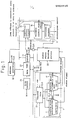
- Figure 1 shows an outline of the construction of an example of an FFP.
- reference numeral 22 is a data RAM, which temporarily stores data provided from a host processor (not shown ) to be used for calculations and the calculation results in the FFP
- reference numeral 23 is an R/W control circuit, which controls the operations of reading from and writing to the data RAM 22.
- the host processor controls the R/W control circuit 23 to write the data to be used for calculations through the data bus 14 into the data RAM 22, and to read the calculation results which are stored in the data RAM 22 after the corresponding calculations are completed.
- Reference numeral 1 is a calculating portion, which comprises a register file 13, a floating point arithmetic logic unit ( hereinafter called ALU ) 12, and a floating point multiplier/divider ( hereinafter called MPY/DIV ) 11.
- ALU floating point arithmetic logic unit
- MPY/DIV floating point multiplier/divider
- the register file 13 reads the data to be used for calculation from the data RAM 22, supplies the data to the ALU 12 or the MPU/DIV 11, and temporarily stores the data during the calculations and the final results of the calculations. The final results are read from the register file 13 and written into the data RAM 22.
- the ALU 12 executes addition/subtraction and comparison/logical calculations
- the MPY/DIV 11 executes multiplication/division calculations.
- Each of the ALU 12 and the MPY/DIV 11 has two output ports, one port of each being used to output the results of the arithmetic calculations like the addition/subtraction or multiplication/division.
- the results of the arithmetic calculations are input to the register file 13.
- the other port of each is used to output status signals, which include the results of the comparison/logical calculations ( hereinafter called non-exception status ), or other status signals showing the type of error which has occurred ( hereinafter called exception status ) when an error (for example, overflow, underflow, input data is not a number, or not normalized, etc. ) occurs during each calculation cycle in the ALU 12 or the MPY/DIV 11.
- Reference numeral 5 is a microprogram controlling portion which controls the execution of the calculations in the FFP and.comprises a sequential control circuit 15, a writable control storage ( hereinafter called WCS ) 16, and a microcode register 17.
- WCS writable control storage
- a microprogram is written into the WCS 16 by the host processor.
- the WCS 16 When an address is output from the sequential control circuit 15, the WCS 16 outputs a microinstruction ( microcode ) which has been written in that address to the microcode register 17.
- the sequential control circuit 15 increments the address to be output when the execution of each microinstruction is completed, and consequently, the microinstruction of the next address is loaded in the microcode register 17.
- a conditional jump instruction is loaded in the microcode register 17, and if the bit of the register 18 is in a predetermined state, the output of the sequential control circuit 15 jumps to the address loaded in'a jump address field.
- the output of the status signal decoding portion 20 is loaded in the register 18.
- the status signal decoding portion 20 inputs the most significant bit ( hereinafter called MSB ) of the data read through the data bus 14 from the .data RAM 22 or from the register file 13, and outputs the status signal instructed to be output by the conditional jump instruction loaded in the microcode register 17, to the register 18.
- MSB most significant bit
- FIG. 2 shows an example of the conventional construction of the status signal decoding portion 20.
- the status signal decoding portion 20 in Fig. 2 comprises a first selector 41, a second selector 8, a decoder 2, and a latch circuit 6.
- the second selector 8 under the microprogram control, selects one of the status signals from the ALU 12 and the status signals from the MPY/DIV 11 at the corresponding timing of the output of the ALU 12 or the MPY/DIV 11.
- the ALU 12 and the MPY/DIV 11 are -controlled so that the ALU 12 and the MPY/DIV 11 do not output effective outputs at the same time.
- the output of the second selector is decoded at the decoder 2, and the corresponding one bit of the outputs of the decoder 2 is made "1", where the outputs of the decoder 2 are provided in correspondence to the types of comparison/logic calculations and the types of errors.
- the group of outputs of the decoder 2 corresponding to the aforementioned non-exception status signals are denoted by D 1
- the group of outputs of the decoder 2 corresponding to the aforementioned exception status signals are denoted by D z.
- the outputs of the decoder belonging to the group D z are directly applied to the first selector 41 in parallel with each other, and the outputs of the decoder belonging to the group D Iare applied to the latch circuit 6 in parallel with each other, held there, and output therefrom to the first selector 41 in parallel with each other and in parallel to the outputs of the decoder belonging to the group D z .
- the MSB of the data from the data RAM 22 or the register file 13 is also applied to the first register 41 through the data bus 14 and in parallel to the above outputs of the decoder 2.
- the microprogram control the instructions included in the conditional jump instructions loaded in the microcode register 17 ), one of the above parallel inputs is selected and is loaded in the register 18.
- the latch circuit 6 is provided because, in general, the abovementioned non-exception status signals are data used in the normal execution processes, e. g., the results of the comparison calculation, or the like, and since a branch instruction depending on such data often consists of a plurality of conditional jump instructions, the data must be held even after the execution of one of the conditional jump instructions is completed.
- the next step is immediately determined, e. g., if it is determined that no error has occurred, the microprogram is then allowed to proceed to the next normal step, or if it is determined that an error has occurred, then, for example, the execution of the FFP must be stopped and the calculation must be re-started from the beginning. Therefore, conventionally, it is deemed not necessary to hold the exception status signals at the latch circuit or the like for checking errors in each calculation in the ALU 12 or the MPY/DIV 11..
- reference numeral 19 in Fig. 2 is an address generator, which generates addresses for the data RAM 22, under the microprogram control.
- the aforementioned jump address field (this consists of 12 bits in the example of Fig. 1 ) in the microcode register 17 is used.
- the jump address field usually is not used except when jump instructions (including the conditional jump instructions ) are executed as mentioned before. Therefore, the jump address field can be used, in addition to the above, to read out the data necessary to generate addresses in the address generator 19 (for example, it may be an output of the address generator 19 ) thereto from the WCS 16, and to output the data to the address generator 19.
- the register 21 data read out from the data RAM 22 can be input to the address generator 19.
- the address generator 19 obtains the address needed to access the data RAM 22, and the data addressed by the output of the address generator 19 is read out from the data RAM 22 under the control of the R/W control circuit 23 according to the microprogram control.
- the status signal decoding portion 20 shown in Fig. 2 when each calculation cycle is completed in the ALU 12 or the MPY/DIV 11, the exception status signal regarding the preceding calculation cycle is renewed, and thus whether or not an error occurred in the preceding'calculation cycle is not memorized. Therefore, to check whether or not an error exists in each calculation cycle, it is necessary to check all the o-utputs of the decoder belonging to the aforementioned group D z by selecting each of the outputs in turn at the first selector 4 for each calculation cycle.
- the conditional jump instructions to select all of the outputs of the decoder belonging to the aforementioned group D z must be loaded in the microcode register 17 in turn for each calculation cycle in the ALU 12 or the MPY/DIV 11.
- the aforementioned jump address field (this consists of 12 bits in the example of Fig. 2 ) is occupied. Therefore, the increase in the number of 'executions of the jump instructions prevents the jump address field from being used for another purpose, ( e. g., sending data to the address generator 19, or the like ).
- An object of the present invention is to provide a fast floating point processor wherein the number of executions of jump instructions in microprogram control is reduced.
- the fast floating point processor comprises a calculating portion which carries out a series of calculations consisting of arithmetic and.comparison/logical calculations under the control by a microprogram controlling portion, and which outputs, for each cycle of the calculations, non-exception status signals which indicate the results of the comparison/logical calculations, or exception status signals each of which indicate an occurrence of an error in the arithmetic or comparison/logical calculations; a decoder which decodes the non-exception status signals and the exception status signals; and a selector which selects one output instructed by the microprogram controlling portion from among the outputs of the decoder; wherein the microprogram controlling portion carries out the controlling operation in accordance with the output of the selector; the fast floating point processor further comprising an error memorizing portion at the input side of the selector, wherein the error memorizing portion memorizes the occurrence of an error in correspondence to each of the outputs corresponding to the exception status signals among the outputs of the decoder until the series of calculations are completed, when an error memorizing portion
- Figure 3 shows the basic construction of the fast floating point processor according to present invention.
- reference numeral 1 is a calculating portion which carries out a series of calculations consisting of arithmetic and comparison/logical calculations under microprogram control, and outputs non-exception status signals which indicate the results of the comparison/logical calculations, or exception status signals each of which indicate an occurrence of an error in the arithmetic or comparison/logical calculations;
- reference numeral 2 is a decoder which decodes the non-exception status signals and the exception status signals;
- reference numeral 4 is a selector which selects one output instructed by the microprogram controlling portion from among the outputs of the decoder 2;
- reference numeral 5 is a microprogram controlling portion which controls the fast floating point processor in accordance with a microprogram and the output of the selector;
- reference numeral 3 is an error memorizing portion which memorizes the occurrence of an error in correspondence to each of the outputs corresponding to the exception status signals among the outputs of the decoder 2 until the
- the non-exception status signal or exception status signal which are output for every calculation cycle during a series of calculations, are decoded at the decoder 2, and whether or not at least one error has occurred during the series of calculations is memorized in the error memorizing portion in correspondence to each of the outputs corresponding to the exception status signals among the outputs of the decoder 2, and therefore, it is possible to check whether or not an error has occurred during the series of calculations in correspondence to each of the outputs corresponding to the exception status signals, by controlling the selector 4 under the control of the microprogram controlling portion 5 when the series of calculations are completed.
- the present invention can reduce the number of executions of conditional jump instructions, compared with the conventional fast floating point processor wherein the microprogram controlling portion 5 controls the selector 4 to check whether or not an error has occurred during each calculation cycle when each calculation cycle is completed, and thus the jump address field in the microcode register which was used for the conditional jump instructions can be used for another purpose, consequently, a degree of freedom in programing is increased.
- Figure 4 shows an example of the construction of the status signal decoding portion 20 in the fast floating point processor (FFP) of Fig. 1, as an embodiment of the present invention.
- FFP fast floating point processor
- each of the outputs D z corresponding to the exception status signals among the outputs of the decoder 2 is connected through the group of flip-flop circuits for exception status 31 to the first selector 41, and each of the outputs of the group of flip-flop registers for exception status 31 is also connected in parallel to the input terminals of the OR circuit 7. Further, the output of the OR circuit 7 is connected to one of the inputs of the first selector 41.
- the above group of flip-flop circuits for exception status 31 consists of a group of set-reset type flip-flop circuits, each of which flip-flop circuits receives the corresponding one of the outputs D z of the decoder 2, which outputs correspond.to the exception status signals, as a set input.
- the occurrence of the error, DIVIDED BY ZERO, is transferred to the status signal decoding portion 20 from the status signal output port of the MPY/DIV 11 in a form of a 4- bits signal.
- This signal is applied to one of two input ports of the second selector 8 of Fig. 4.
- the second selector 8 is controlled by the microprogram to select the output of the MPY/DIV 11 at the timing at which status signals are output from the MPY/DIV 11.
- the signal in the form of a 4-bits signal from the MPY/DIV 11 showing the occurrence of the error, DIVIDED BY ZERO is input to the decoder 2.
- the decoder decodes the signal, and accordingly, makes the state of the corresponding output ( one among the outputs D z corresponding to the aforementioned exception status signals, because DIVIDED BY ZERO is an error state ) "1".
- the output of the decoder 2 corresponding to the state DIVIDED BY ZERO is input to the corresponding flip-flop circuit in the aforementioned group of flip-flop circuits for exception status 31, sets the flip-flop circuit, and the output of the flip-flop circuit is held in the "I” state.
- the output of the flip-flop circuit "1" is input to both the first selector 41 and the OR circuit 7, and accordingly, the output of the OR circuit 7 is also held in the "I” state, since one of the inputs is held in the "1" state.
- the first selector 41 selects the output of the OR circuit 7 in accordance with the microprogram control ( by a conditional jump instruction loaded on the microcode register 17 in Fig. 1 ). If the output of the OR circuit 7 is "0", it is recognized that no error has occurred during the series of calculations in the MPY/DIV 11 and the ALU 12. If the output of the OR circuit 7 is "1", it is recognized that at least one error has occurred during the series of calculations, and accordingly, the microprogram controlling portion 5 controls the first selector 41 to select each of the outputs of the group of flip-flop circuits for exception status 31 in turn, and thereby confirms the kind of error that has occurred.
- the present invention reduces the number of executions of jump instructions in microprogram control of fast floating point processors, and the jump address field in the microcode register formerly used for the - 'conditional jump instructions can be used for another purpose.
- the present invention is useful when applied to fast floating point processors under microprogram control.
Abstract
57 A high-speed floating point arithmetic unit for microprogram-controlled arithmetic and comparation/logic operations, comprising a decoder (2) for various status signals including one indicating the generation of error in the arithmetic section (1), and a selector (4) for selecting one of the outputs of the decoder (2) based on microprogram control. In a stage preceding the selector (4) there is further provided an error memory (3) for storing information about the presence of an error during a series of operations, said information corresponding to each of the error-involving outputs from the decoder (2).
Description
- The present invention relates to a fast floating point processor.
- As the speed of floating point calculation is very slow in general purpose processors, fast floating point processors ( hereinafter called FFP ) which use a hardware construction for floating point calculation only, are used for that purpose.
- Figure 1 shows an outline of the construction of an example of an FFP.
- . In Fig, 1,
reference numeral 22 is a data RAM, which temporarily stores data provided from a host processor ( not shown ) to be used for calculations and the calculation results in the FFP, andreference numeral 23 is an R/W control circuit, which controls the operations of reading from and writing to thedata RAM 22. The host processor controls the R/W control circuit 23 to write the data to be used for calculations through thedata bus 14 into thedata RAM 22, and to read the calculation results which are stored in thedata RAM 22 after the corresponding calculations are completed. -
Reference numeral 1 is a calculating portion, which comprises aregister file 13, a floating point arithmetic logic unit ( hereinafter called ALU ) 12, and a floating point multiplier/divider ( hereinafter called MPY/DIV ) 11. - According to the microprogram control ( described later ), the
register file 13 reads the data to be used for calculation from thedata RAM 22, supplies the data to theALU 12 or the MPU/DIV 11, and temporarily stores the data during the calculations and the final results of the calculations. The final results are read from theregister file 13 and written into thedata RAM 22. - The
ALU 12 executes addition/subtraction and comparison/logical calculations, and the MPY/DIV 11 executes multiplication/division calculations. Each of theALU 12 and the MPY/DIV 11 has two output ports, one port of each being used to output the results of the arithmetic calculations like the addition/subtraction or multiplication/division. The results of the arithmetic calculations are input to theregister file 13. The other port of each is used to output status signals, which include the results of the comparison/logical calculations ( hereinafter called non-exception status ), or other status signals showing the type of error which has occurred ( hereinafter called exception status ) when an error ( for example, overflow, underflow, input data is not a number, or not normalized, etc. ) occurs during each calculation cycle in theALU 12 or the MPY/DIV 11. -
Reference numeral 5 is a microprogram controlling portion which controls the execution of the calculations in the FFP and.comprises asequential control circuit 15, a writable control storage ( hereinafter called WCS ) 16, and amicrocode register 17. - At the beginning of the execution of the calculations in the FFP, a microprogram is written into the WCS 16 by the host processor. When an address is output from the
sequential control circuit 15, theWCS 16 outputs a microinstruction ( microcode ) which has been written in that address to themicrocode register 17. Usually, thesequential control circuit 15 increments the address to be output when the execution of each microinstruction is completed, and consequently, the microinstruction of the next address is loaded in themicrocode register 17. When a conditional jump instruction is loaded in themicrocode register 17, and if the bit of theregister 18 is in a predetermined state, the output of thesequential control circuit 15 jumps to the address loaded in'a jump address field. The output of the statussignal decoding portion 20 is loaded in theregister 18. - The status
signal decoding portion 20 inputs the most significant bit ( hereinafter called MSB ) of the data read through thedata bus 14 from the.data RAM 22 or from theregister file 13, and outputs the status signal instructed to be output by the conditional jump instruction loaded in themicrocode register 17, to theregister 18. - Figure 2 shows an example of the conventional construction of the status
signal decoding portion 20. - The status
signal decoding portion 20 in Fig. 2 comprises afirst selector 41, asecond selector 8, adecoder 2, and alatch circuit 6. Thesecond selector 8, under the microprogram control, selects one of the status signals from theALU 12 and the status signals from the MPY/DIV 11 at the corresponding timing of the output of theALU 12 or the MPY/DIV 11. In the example of the Fig. 1, it is assumed that theALU 12 and the MPY/DIV 11 are -controlled so that theALU 12 and the MPY/DIV 11 do not output effective outputs at the same time. - The output of the second selector is decoded at the
decoder 2, and the corresponding one bit of the outputs of thedecoder 2 is made "1", where the outputs of thedecoder 2 are provided in correspondence to the types of comparison/logic calculations and the types of errors. - In fig. 2, the group of outputs of the
decoder 2 corresponding to the aforementioned non-exception status signals are denoted by D1, and the group of outputs of thedecoder 2 corresponding to the aforementioned exception status signals are denoted by D z. - In the construction of Fig. 2, the outputs of the decoder belonging to the group Dz are directly applied to the
first selector 41 in parallel with each other, and the outputs of the decoder belonging to the group D Iare applied to thelatch circuit 6 in parallel with each other, held there, and output therefrom to thefirst selector 41 in parallel with each other and in parallel to the outputs of the decoder belonging to the group Dz. The MSB of the data from thedata RAM 22 or theregister file 13 is also applied to thefirst register 41 through thedata bus 14 and in parallel to the above outputs of thedecoder 2. According to the microprogram control ( the instructions included in the conditional jump instructions loaded in the microcode register 17 ), one of the above parallel inputs is selected and is loaded in theregister 18. - The
latch circuit 6 is provided because, in general, the abovementioned non-exception status signals are data used in the normal execution processes, e. g., the results of the comparison calculation, or the like, and since a branch instruction depending on such data often consists of a plurality of conditional jump instructions, the data must be held even after the execution of one of the conditional jump instructions is completed. - On the other hand, regarding the group of outputs of the decoder denoted by the Dz corresponding to the exception status, in general, whether or not at least one error has occurred is once determined, then the next step is immediately determined, e. g., if it is determined that no error has occurred, the microprogram is then allowed to proceed to the next normal step, or if it is determined that an error has occurred, then, for example, the execution of the FFP must be stopped and the calculation must be re-started from the beginning. Therefore, conventionally, it is deemed not necessary to hold the exception status signals at the latch circuit or the like for checking errors in each calculation in the
ALU 12 or the MPY/DIV 11.. - Further,
reference numeral 19 in Fig. 2 is an address generator, which generates addresses for thedata RAM 22, under the microprogram control. To generate the addresses, the aforementioned jump address field ( this consists of 12 bits in the example of Fig. 1 ) in themicrocode register 17 is used. The jump address field usually is not used except when jump instructions ( including the conditional jump instructions ) are executed as mentioned before. Therefore, the jump address field can be used, in addition to the above, to read out the data necessary to generate addresses in the address generator 19 ( for example, it may be an output of the address generator 19 ) thereto from theWCS 16, and to output the data to theaddress generator 19. Alternatively, by using theregister 21, data read out from thedata RAM 22 can be input to theaddress generator 19. By using the above data, and if necessary, by some calculation, theaddress generator 19 obtains the address needed to access thedata RAM 22, and the data addressed by the output of theaddress generator 19 is read out from thedata RAM 22 under the control of the R/W control circuit 23 according to the microprogram control. - By the construction of the status
signal decoding portion 20 shown in Fig. 2, when each calculation cycle is completed in theALU 12 or the MPY/DIV 11, the exception status signal regarding the preceding calculation cycle is renewed, and thus whether or not an error occurred in the preceding'calculation cycle is not memorized. Therefore, to check whether or not an error exists in each calculation cycle, it is necessary to check all the o-utputs of the decoder belonging to the aforementioned group Dz by selecting each of the outputs in turn at thefirst selector 4 for each calculation cycle. - More concretely, to carry out the above operation, the conditional jump instructions to select all of the outputs of the decoder belonging to the aforementioned group Dz must be loaded in the
microcode register 17 in turn for each calculation cycle in theALU 12 or the MPY/DIV 11. As mentioned before, when a jump instruction is loaded in themicrocode register 17, the aforementioned jump address field ( this consists of 12 bits in the example of Fig. 2 ) is occupied. Therefore, the increase in the number of 'executions of the jump instructions prevents the jump address field from being used for another purpose, ( e. g., sending data to theaddress generator 19, or the like ). - An object of the present invention is to provide a fast floating point processor wherein the number of executions of jump instructions in microprogram control is reduced.
- The fast floating point processor according to the present invention comprises a calculating portion which carries out a series of calculations consisting of arithmetic and.comparison/logical calculations under the control by a microprogram controlling portion, and which outputs, for each cycle of the calculations, non-exception status signals which indicate the results of the comparison/logical calculations, or exception status signals each of which indicate an occurrence of an error in the arithmetic or comparison/logical calculations; a decoder which decodes the non-exception status signals and the exception status signals; and a selector which selects one output instructed by the microprogram controlling portion from among the outputs of the decoder; wherein the microprogram controlling portion carries out the controlling operation in accordance with the output of the selector; the fast floating point processor further comprising an error memorizing portion at the input side of the selector, wherein the error memorizing portion memorizes the occurrence of an error in correspondence to each of the outputs corresponding to the exception status signals among the outputs of the decoder until the series of calculations are completed, when an error has occurred during the series of calculations.
-
- Figure 1 shows an outline of the construction of an example of fast floating point processor (FFP);
- Figure 2 shows a conventional construction of the status
signal decoding portion 20 in Fig. 1; - Figure 3 shows the basic construction of the present invention; and,
- Figure 4 shows an example of the construction of the status
signal decoding portion 20 in the fast floating point processors (FFP) of Fig. 1, as an embodiment of the present invention. - Figure 3 shows the basic construction of the fast floating point processor according to present invention. In Fig. 3,
reference numeral 1 is a calculating portion which carries out a series of calculations consisting of arithmetic and comparison/logical calculations under microprogram control, and outputs non-exception status signals which indicate the results of the comparison/logical calculations, or exception status signals each of which indicate an occurrence of an error in the arithmetic or comparison/logical calculations;reference numeral 2 is a decoder which decodes the non-exception status signals and the exception status signals;reference numeral 4 is a selector which selects one output instructed by the microprogram controlling portion from among the outputs of thedecoder 2;reference numeral 5 is a microprogram controlling portion which controls the fast floating point processor in accordance with a microprogram and the output of the selector; andreference numeral 3 is an error memorizing portion which memorizes the occurrence of an error in correspondence to each of the outputs corresponding to the exception status signals among the outputs of thedecoder 2 until the series of calculations are completed, when one error has occurred during the series of calculations. - In the fast floating point processor according to the present invention, the non-exception status signal or exception status signal, which are output for every calculation cycle during a series of calculations, are decoded at the
decoder 2, and whether or not at least one error has occurred during the series of calculations is memorized in the error memorizing portion in correspondence to each of the outputs corresponding to the exception status signals among the outputs of thedecoder 2, and therefore, it is possible to check whether or not an error has occurred during the series of calculations in correspondence to each of the outputs corresponding to the exception status signals, by controlling theselector 4 under the control of themicroprogram controlling portion 5 when the series of calculations are completed. - Accordingly, the present invention can reduce the number of executions of conditional jump instructions, compared with the conventional fast floating point processor wherein the
microprogram controlling portion 5 controls theselector 4 to check whether or not an error has occurred during each calculation cycle when each calculation cycle is completed, and thus the jump address field in the microcode register which was used for the conditional jump instructions can be used for another purpose, consequently, a degree of freedom in programing is increased. - Figure 4 shows an example of the construction of the status
signal decoding portion 20 in the fast floating point processor (FFP) of Fig. 1, as an embodiment of the present invention. - Although the construction of the status
signal decoding portion 20 in Fig. 4, which consists of afirst selector 41, asecond selector 8, adecoder 2, and alatch circuit 6, is the same as the corresponding construction in the statussignal decoding portion 20 in Fig. 2, each of the outputs Dz corresponding to the exception status signals among the outputs of thedecoder 2 is connected through the group of flip-flop circuits forexception status 31 to thefirst selector 41, and each of the outputs of the group of flip-flop registers forexception status 31 is also connected in parallel to the input terminals of theOR circuit 7. Further, the output of theOR circuit 7 is connected to one of the inputs of thefirst selector 41. - The above group of flip-flop circuits for
exception status 31 consists of a group of set-reset type flip-flop circuits, each of which flip-flop circuits receives the corresponding one of the outputs D z of thedecoder 2, which outputs correspond.to the exception status signals, as a set input. For example, if, for one microcycle, "1" is input from one of the above outputs Dz of the decoder to the group of flip-flop registers forexception status 31, the flip-flop circuit corresponding to the above one of the outputs D z in the group of flip-flop registers forexception status 31 is set, and then the output of the flip-flop circuit is held until the flip-flop circuit is reset, regardless of the state of the above one of the outputs Dz in the following microcycles. The reset terminals of these elements, each of which functions as a set-reset type flip-flop circuit as mentioned above, are connected to a common CLEAR input, and all of the elements operate synchronously with a clock pulse (CLK). - An example of the operation of the abovementioned status
signal decoding portion 20 is explained hereinafter with reference to Figs. 4 and 1. - Assuming that the data input to the floating point multiplier/divider (MPY/DIV) 11 is .0., the occurrence of the error, DIVIDED BY ZERO, is transferred to the status
signal decoding portion 20 from the status signal output port of the MPY/DIV 11 in a form of a 4- bits signal. This signal is applied to one of two input ports of thesecond selector 8 of Fig. 4. As the MPY/DIV 11 andALU 12 are controlled so that theALU 12 and the MPY/DIV 11 do not output effective outputs at the same time, thesecond selector 8 is controlled by the microprogram to select the output of the MPY/DIV 11 at the timing at which status signals are output from the MPY/DIV 11. Accordingly, the signal in the form of a 4-bits signal from the MPY/DIV 11 showing the occurrence of the error, DIVIDED BY ZERO, is input to thedecoder 2. The decoder decodes the signal, and accordingly, makes the state of the corresponding output ( one among the outputs Dz corresponding to the aforementioned exception status signals, because DIVIDED BY ZERO is an error state ) "1". The output of thedecoder 2 corresponding to the state DIVIDED BY ZERO is input to the corresponding flip-flop circuit in the aforementioned group of flip-flop circuits forexception status 31, sets the flip-flop circuit, and the output of the flip-flop circuit is held in the "I" state. The output of the flip-flop circuit "1" is input to both thefirst selector 41 and theOR circuit 7, and accordingly, the output of theOR circuit 7 is also held in the "I" state, since one of the inputs is held in the "1" state. - When a series of calculations are completed, the
first selector 41 selects the output of theOR circuit 7 in accordance with the microprogram control ( by a conditional jump instruction loaded on themicrocode register 17 in Fig. 1 ). If the output of theOR circuit 7 is "0", it is recognized that no error has occurred during the series of calculations in the MPY/DIV 11 and theALU 12. If the output of theOR circuit 7 is "1", it is recognized that at least one error has occurred during the series of calculations, and accordingly, themicroprogram controlling portion 5 controls thefirst selector 41 to select each of the outputs of the group of flip-flop circuits forexception status 31 in turn, and thereby confirms the kind of error that has occurred. - As mentioned above, by applying the status
signal decoding portion 20 as shown in Fig. 4 to the construction of FFP as shown in Fig. 1, it becomes possible to check whether or not at least one error has occurred in the MPY/DIV 11 and theALU 12, by one operation under the microprogram control at the time at which a series of calculations in the MPY/DIV 11 and theALU 12 are completed. - As described hitherto, the present invention reduces the number of executions of jump instructions in microprogram control of fast floating point processors, and the jump address field in the microcode register formerly used for the-'conditional jump instructions can be used for another purpose.
- The present invention is useful when applied to fast floating point processors under microprogram control.
Claims (2)
1. A fast floating point processor comprising: a calculating portion (1) which carries out a series of calculations consists of arithmetic and comparison/logic al calculations under the control of a microprogram controlling portion (5), and outputs, for each cycle of said calculations, non-exception status signals which indicate the results of the comparison/logical calculations, or exception status signals each of which indicates an occurrence of error in said arithmetic and comparison/logical calculations; a decoder (2) which decodes said non-exception status signals and said exception status signals; and a selector (4) which selects one output instructed by said microprogram controlling portion (5) to be selected from among the outputs of said decoder (2); wherein said microprogram controlling portion (5) carries out a control operation in accordance with an output of said selector (4); the fast floating point processor further comprising an error memorizing portion (3) in an input side of said selector (4), said error memorizing portion (3) memorizing an occurrence of an error in correspondence to each of the outputs corresponding to said exception status signals among outputs of said decoder (2) until said series of calculations is completed, when an error has occurred during said series of calculations.
2. A fast floating point processor according to claim 1, wherein the outputs of said error memorizing portion (3) are connected in parallel with each other to an OR circuit (7), and the output of said OR circuit (7) is also connected to one input of said selector (4).
Applications Claiming Priority (2)
| Application Number | Priority Date | Filing Date | Title |
|---|---|---|---|
| JP62052217A JPS63219031A (en) | 1987-03-09 | 1987-03-09 | High speed floating point computing element |
| JP52217/87 | 1987-03-09 |
Publications (1)
| Publication Number | Publication Date |
|---|---|
| EP0305530A1 true EP0305530A1 (en) | 1989-03-08 |
Family
ID=12908584
Family Applications (1)
| Application Number | Title | Priority Date | Filing Date |
|---|---|---|---|
| EP19880901465 Withdrawn EP0305530A1 (en) | 1987-03-09 | 1988-02-08 | High-speed floating point arithmetic unit |
Country Status (3)
| Country | Link |
|---|---|
| EP (1) | EP0305530A1 (en) |
| JP (1) | JPS63219031A (en) |
| WO (1) | WO1988007237A1 (en) |
Families Citing this family (1)
| Publication number | Priority date | Publication date | Assignee | Title |
|---|---|---|---|---|
| US8397187B2 (en) | 2010-04-23 | 2013-03-12 | International Business Machines Corporation | Verifying the error bound of numerical computation implemented in computer systems |
Family Cites Families (3)
| Publication number | Priority date | Publication date | Assignee | Title |
|---|---|---|---|---|
| JPS51146143A (en) * | 1975-06-11 | 1976-12-15 | Hitachi Ltd | Wedging process mode when logic device generates error action |
| JPS6388636A (en) * | 1986-10-01 | 1988-04-19 | Nec Corp | Microcomputer |
| JPS63178330A (en) * | 1987-01-20 | 1988-07-22 | Toshiba Corp | Operation flag controller |
-
1987
- 1987-03-09 JP JP62052217A patent/JPS63219031A/en active Pending
-
1988
- 1988-02-08 EP EP19880901465 patent/EP0305530A1/en not_active Withdrawn
- 1988-02-08 WO PCT/JP1988/000117 patent/WO1988007237A1/en not_active Application Discontinuation
Non-Patent Citations (1)
| Title |
|---|
| See references of WO8807237A1 * |
Also Published As
| Publication number | Publication date |
|---|---|
| JPS63219031A (en) | 1988-09-12 |
| WO1988007237A1 (en) | 1988-09-22 |
Similar Documents
| Publication | Publication Date | Title |
|---|---|---|
| US4430706A (en) | Branch prediction apparatus and method for a data processing system | |
| US5511207A (en) | Program control circuit determining the designated number of times a sequence of instructions is repetitively executed to prevent further execution of a jump instruction | |
| EP0155211B1 (en) | System for by-pass control in pipeline operation of computer | |
| JP2539199B2 (en) | Digital processor controller | |
| EP0111776B1 (en) | Interrupt processor | |
| US4542456A (en) | Method and apparatus for performing range checks | |
| GB1274830A (en) | Data processing system | |
| US4541045A (en) | Microprocessor architecture employing efficient operand and instruction addressing | |
| US4446517A (en) | Microprogram memory with page addressing and address decode in memory | |
| EP0094535B1 (en) | Pipe-line data processing system | |
| US4739470A (en) | Data processing system | |
| EP0223150B1 (en) | Information processing apparatus | |
| EP0010196B1 (en) | Control circuit and process for digital storage devices | |
| US5247624A (en) | Microprogram controller including leading microinstruction from a generator executed while succeeding microinstruction from memory is read out | |
| US4093983A (en) | Fast and normal rate instruction fetching | |
| JPS59116855A (en) | Control memory mechanism | |
| EP0164418B1 (en) | Microprogram control system | |
| EP0305530A1 (en) | High-speed floating point arithmetic unit | |
| CA1119307A (en) | Microcomputer having separate bit and word accumulators and separate bit and word instruction sets | |
| US8200943B2 (en) | Microprocessor | |
| US5828859A (en) | Method and apparatus for setting the status mode of a central processing unit | |
| EP0166772B1 (en) | Improvements in or relating to computer systems | |
| KR910001708B1 (en) | Central processing unit | |
| EP0343668B1 (en) | Normalization control system for floating point arithmetic operations | |
| EP0306533A1 (en) | High-speed floating point operation system |
Legal Events
| Date | Code | Title | Description |
|---|---|---|---|
| PUAI | Public reference made under article 153(3) epc to a published international application that has entered the european phase |
Free format text: ORIGINAL CODE: 0009012 |
|
| 17P | Request for examination filed |
Effective date: 19881207 |
|
| AK | Designated contracting states |
Kind code of ref document: A1 Designated state(s): DE FR GB |
|
| 18W | Application withdrawn |
Withdrawal date: 19891215 |
|
| STAA | Information on the status of an ep patent application or granted ep patent |
Free format text: STATUS: THE APPLICATION HAS BEEN WITHDRAWN |
|
| R18W | Application withdrawn (corrected) |
Effective date: 19891215 |