EP0304285A2 - Network control system - Google Patents
Network control system Download PDFInfo
- Publication number
- EP0304285A2 EP0304285A2 EP88307621A EP88307621A EP0304285A2 EP 0304285 A2 EP0304285 A2 EP 0304285A2 EP 88307621 A EP88307621 A EP 88307621A EP 88307621 A EP88307621 A EP 88307621A EP 0304285 A2 EP0304285 A2 EP 0304285A2
- Authority
- EP
- European Patent Office
- Prior art keywords
- bit
- node
- link
- links
- input
- Prior art date
- Legal status (The legal status is an assumption and is not a legal conclusion. Google has not performed a legal analysis and makes no representation as to the accuracy of the status listed.)
- Granted
Links
Images


Classifications
-
- G—PHYSICS
- G06—COMPUTING; CALCULATING OR COUNTING
- G06F—ELECTRIC DIGITAL DATA PROCESSING
- G06F15/00—Digital computers in general; Data processing equipment in general
- G06F15/16—Combinations of two or more digital computers each having at least an arithmetic unit, a program unit and a register, e.g. for a simultaneous processing of several programs
- G06F15/163—Interprocessor communication
- G06F15/173—Interprocessor communication using an interconnection network, e.g. matrix, shuffle, pyramid, star, snowflake
- G06F15/17337—Direct connection machines, e.g. completely connected computers, point to point communication networks
- G06F15/17343—Direct connection machines, e.g. completely connected computers, point to point communication networks wherein the interconnection is dynamically configurable, e.g. having loosely coupled nearest neighbor architecture
Definitions
- the present invention relates to a network control system in a hyper cube type network used in a multi-processors interconnection system.
- the hyper cube type network is constituted by a plurality of nodes (2 n nodes, n > 0, integer), each node being arranged on an apex of the cube, a plurality of links connecting the nodes, and a plurality of processors, each connected to each node.
- multi-processors interconnection system two types, i.e., a multi-stage network and a multi-processors network.
- the multi-stage network includes various types of networks based on differences in the connection configuration thereof.
- an omega network for example, a delta network, a banyan network, a shuffle-exchange network, etc.
- these types for example, the omega network and the shuffle-exchange network, have a plurality of switch boxes, and each switch box generally has two input terminals and two output terminals.
- Each switch box can take two connection configurations, i.e., cross and straight corresponding to a bit "1" and a bit "0".
- the switch boxes are connected by links from input stages to output stages in accordance with the above connection configurations, to form communication paths.
- the multi-processor network is constituted by a plurality of nodes and links connected between the nodes, wherein each node has at least one buffer memory for temporarily storing input messages.
- This type of network is constituted by a ring type, tree type, hyper cube type, etc., in accordance with different arrangements of the nodes.
- the hyper cube type network can be obtained in both the multi-stage and the multi-processor type of network, in the connection configuration of the nodes and the links, by rewriting a topology thereof. That is, the network having the hyper cube topology exists in the multi-stage and multi-processor networks. In this case, it is possible to modify the shuffle-exchange network to the hyper cube topology by rewriting the structure thereof when the former does not have the hyper cube topology.
- the all-to-all burst communication is a communication pattern in which each processor can simultaneously communicate to all processors including oneself in the system. Therefore, in the present invention, all communication paths are previously scheduled to achieve an effective all-to-all burst communication in the hyper cube type network.
- the multi-stage network is disclosed in, New Generation Computing, 1984, "A Multi Page-Memory Architecture and A Multiport Disk-Cache System", by Yuzuru Tanaka.
- This network is constituted by a plurality of ports, a plurality of memory banks, a plurality of switch boxes, and a controller.
- the controller controls the connection of switch boxes based on a predetermined control program.
- the network is formed between the ports and the memory banks.
- the topology of the network is the type of the shuffle-exchange network, and the switch box comprises two inputs and two outputs.
- a network control system in a hyper cube type network constituted by: 2 n nodes (n > 0, integer), each node being arranged on an apex of a cube and having n sets of links for interconnecting other nodes to form an n-dimensional hyper cube type network; and a plurality of processors, each processor being connected to a said node by input/output links, thereby providing communication paths between processors through the nodes and links; each of the nodes comprising, a device for setting 2 n different connection patterns corresponding to 2 n phase signals, and a switching device for interconnecting between the links and between the input/output links in accordance with the connection patterns synchronized with the phase signals.
- Each node is designated by binary numbers "000", "001" --- "111", has three links, and is connected to another node based on the following connection rule.
- the first bit of the node designation of the node 1 is different from that of the node 2, and thus the link 1 of the node 1 is connected to the link 1 of the node 2.
- the second bit of the node designation of the node 1 is different from that of the node 3, and accordingly, the link 2 of the node 1 is connected to the link 2 of the node 3.
- the third bit of the node designation of the node 1 is different from that of the node 5, and therefore, the link 3 of the node 1 is connected to the link 3 of the node 5.
- the same rule is applied to the other nodes, and thus all of the nodes are connected to each other in such a manner that they constitute a three-dimensional hyper cube type network.
- 2 n nodes are distinguished by 2 n node designations.
- Each of the node designations can be expressed by a binary number having n bits in the n-dimensional hyper cube type network.
- each node is connected to the other n nodes.
- Figure 2 is a schematic block diagram of a prior proposed node. This node is used in a multi-processors network.
- reference number 10 denotes a reception control unit, 11 a transmission control unit, 12 an input control unit, 13 an output control unit, 14 a buffer memory, 15 a router, and 16 a bus line.
- the input control unit 12 and the output control unit 13 are connected to the processor (not shown), for controlling the reception or transmission of messages from or to the processor.
- the reception control unit 10 and the transmission control unit 11 are connected to the link for controlling the transmission and reception of messages from another node.
- the buffer memory 14 temporarily stores transmission and reception messages, and the router 15 distinguishes an address of the message and controls another node to which it is to be relayed.
- the reception control unit 10 and the input control unit 12 transfer messages input from the processor and the link, and the buffer memory 14 stores the messages to the predetermined memory area.
- the transmission control unit 11 and the output control unit 13 transfer the messages read out from the memory area under the control of the router 15.
- the router 15 comprises a suitable processing means for running a control program, and accordingly, based on the control program, the router 15 distinguishes the node designation of the destination of the received message, determines the transmission destination to which it is to be relayed, and sends a command concerning the destination to the transmission control unit 11 and the output control unit 13.
- the message from the processor has the node designation of the destination at the head thereof, and the input control unit 12 informs the router 15 that the message has been stored.
- the router 15 compares the node designation of the destination of the received message stored in the buffer memory 14 with the own node designation. If the former coincides with the latter, the destination of the received message is determined to be the own node. In this case, the received message is output to the processor connected to the own node through the transmission control unit 11.
- the received message is output to another node having the number corresponding to the inconsistent bit of the former and the latter.
- the above node is applied to the hyper cube type network shown in Fig. 1, if the message is transmitted from the node 1 (000) to the node 6 (101) through the link (indicated by thick lines), the message from the processor connected to the node 1 is temporarily stored in the buffer memory 14 of the node 1.
- the router 15 compares the node designation "101" of the destination node 6 with the own node designation "000" of the node 1 and determines the link to be selected. In this case, since the first and the third bits of the node designation "000" and the node designation "101" are different, the link denoted by the thick line is selected.
- the router 15 of the node 1 selects the third link
- the message is transferred from the buffer memory 14 of the node 1 to the third link through the transmission control unit 11, and the message is stored in the buffer memory 14 of the node 5 through the reception control unit 10 therein.
- the router 15 of the node 5 compares the node designation "101" of the destination node 6 with the own node designation "100" of the node 5, and determines the link to be selected. In this case, since the first bit is different in the node designation "101", the message is transferred from the buffer memory 14 of the node 5 to the first link through the transmission control unit 11 therein.
- the message is stored in the buffer memory 14 of the node 6 through the reception control unit 10 therein, the router 15 of the node 6 distinguishes that the message designates the own node designation "101", and the message is then transferred to the processor connected to the node 6 through the output control unit 13 therein.
- the message quantities passing through each of the links are unbalanced so that a complex relation- ship of busy links and not-busy links exists in the network since it is not possible to make completely uniform the message quantities passing through each link.
- a router having a higher processing performance must be provided in each node, to process many messages passing through the link, and accordingly, the manufacturing cost per node is increased.
- Figure 3 is a basic structural view of a node embodying the present invention.
- a plurality of nodes are connected to each other through links in such a manner that they form the hyper cube type network shown in Fig. 1.
- reference number 20 denotes a node, 21 a switch unit, 22 links, 23 input links, 24 output links, 25 a connection pattern setting unit and 26 a phase signal.
- Each link 22 is connected to another node, and the input link 23 and the output link 24 are connected to the processor.
- the switch unit 21 is connected to the link 22, the input link 23, and the output link 24, and switches the interconnection among these links in accordance with the connection pattern set by the setting unit 25 synchronized with the phase signal 26.
- the node 20 is one of 2 n nodes, each having the same structure in the n-dimensional hyper cube type network, and each node 20 is connected by n sets of links 22 to the other n nodes.
- the connection pattern setting unit 25 determines 2 n connection patterns synchronized with the phase signal 26.
- one period is constituted by 2 n phases simultaneously supplied to all nodes.
- One phase signal contains n messages and can process 2 n messages, and accordingly, the all-to-all burst communication is processed by 2 n phases.
- the switch unit 21 controls 2 n kinds of connections during one period to interconnect the link 22 and the input link 23, and the link 22 and the output link 24, based on the connection patterns supplied from the unit 25.
- the busy state and waiting state of the link when relaying the message do not occur in the network without congestion of the message at the communication path, so that the processing performance of the network can be raised when performing an all-to-all burst communication.
- Figure 4 is one example of the connection of a four-dimensional hyper cube type network.
- the binary number (0000, 0001 ---) at each node is the node designation, and the number at each line is the link number.
- Figure 5 is a schematic block diagram of a node according to one embodiment of the present invention.
- reference number 30 denotes a node, 31 to 34 links, 35 an input link, 36 and 37 two output links, 39 an input line, 40 a switch unit, 41 a control unit, 42 a buffer memory, 43 a connection pattern setting unit, 44 a register, 50 a global controller, 51 a bit train generator, 52 a signal line, 53 an invertor, and 54 a signal line.
- the node 30 is connected to the links 31 to 34 and to the processor through the input link 35 and two output links 36, 37.
- the input link 35 is connected to the switch unit 40 through the buffer 42 and the input line 39.
- the messages are temporarily stored in the buffer 42 and sequentially read out from the buffer 42 to the switch unit 40 through the input signal line 39.
- the buffer 42 has, for example, sixteen memory areas corresponding to the sixteen nodes shown in Fig. 4, and temporarily stores each message to be transferred from the processor to each node.
- the control unit 41 controls the connection configuration at the switch unit 40 and selection of the message read out from the buffer 42 based on the connection patterns supplied from the connection pattern setting unit 43 and the own node designation held in the register 44.
- the global controller 50 comprises the bit train generator 51 and the invertor 53, and is provided in common in the hyper cube network.
- the bit train generator 51 generates different bit trains at constant time intervals set as being sufficient for transferring one message. This bit train is transferred to all nodes having an even node designation through the signal line 52, and simultaneously, the bit train inverted by the invertor 53 is transferred to all nodes having an odd node designation through the signal line 54.
- the bit train generator 51 can generate 2 n kinds of bit trains during one period.
- the even node designations are those containing zero or even numbers of the bit "1" in the bit train
- the odd node designations are those containing odd numbers of the bit "1" in the bit train; for example, the node designations "0000", “0101", “1111”, etc., are even node designations, and the node designations "0001", “1011”, etc., are odd designations.
- the control unit 41 decodes the connection pattern from the con- nection pattern setting unit 43 and generates the predetermined control signal.
- connection rule at the switch unit 40 is briefly explained hereinafter.
- the interconnection between the links and between the input/output links is performed in such a way that, each of bits from the first to n'th of the connection pattern is corresponded to each of links from the first to n'th, respectively, the input link is connected to the link corresponding to the most significant bit of the bit "1" contained in the connection pattern, the remaining bits “1” are paired from the upper bit and each pair of link is connected to corresponding each pair of bit, respectively, and the bits "0" contained in the connection pattern are paired from the upper bit and each pair of link is connected to corresponding each pair of bit, respectively; further, when the bit "1" does not exist in the connection pattern, the input link is connected to the output link 36; when even numbers of the bit "1” exist in the connection pattern, the bit “1” of the least significant bit disconnected by the above connection manner is connected to the output link 36, then, when odd numbers of the bit "1” exist in the connection pattern, the bit “0” of the least significant bit disconnected by the above connection manner is connected to the output link
- Figure 6 is a view for explaining the connection configuration of the switch unit corresponding to each connection pattern.
- reference numbers 1 to 4 denote links corresponding to links 31 to 34 in Fig. 5
- "I” denotes an input line corresponding to the input line 39
- "O1" and “O2” denote two output lines corresponding to the output lines 36 and 37.
- control unit 41 in Fig. 5 obtains an "exclusive OR" between the connection pattern and the own node designation of the register 44, as the node designation of the destination, and transfers the exclusive OR as the control signal to the buffer 42, where the message at the area assigned by the destination is read out from the buffer and transferred to the input line 39.
- connection pattern when the connection pattern is "0011", the node having an even node designation, for example, "1001", is connected to the node designated "1010", as shown by the thick lines in Fig. 4.
- the connection configuration of the connection pattern "0011” is shown in Fig. 6.
- the input line I is connected to the first link 1 so that the input message is transferred to the node designated "1000" shown in Fig. 4.
- connection pattern "1100" is used as the connection pattern.
- the connection pattern "1100” is shown in Fig. 6. That is, the first link 1 is connected to the second link 2 so that the message input from the first link 1 is transferred to the second link 2 and further transferred to the node designated "1010".
- connection pattern "0011” is used in the node designation "1010" since this is an even node designation.
- the connection configuration of the connection pattern "0011” is shown in Fig. 6, as already explained. That is, the second link 2 is connected to the output O1. Accordingly, the message input from the processor of the node designated "1001" is transferred to the processor of the node designated "1010".
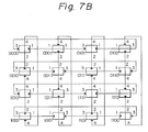
- Figures 7A, 7B and 7C are views for explaining various communication paths in the hyper cube network.
- Fig. 7A shows the case where the connection pattern at the even node designation is "0010”
- Fig. 7B shows the case where the designation is "0101”
- Fig. 7C shows the case where the designation is "1111”.
- the connection patterns at the odd node designations are "1101”, “1010”, and "0000", respectively.
- both output lines O1 and O2 are used in a certain node and not used in the remaining nodes.
- Figure 8 is a schematic block diagram of the node according to another embodiment of the present invention.
- reference number 60 denotes a node, 61a to 64b links, 65 to 68 switch boxes, 69 a buffer memory, 73 to 75 input signal lines, and 72 a control unit.
- Each of the switch boxes 65 to 68 is connected to each of a pair of links 61a and 61b, 62a and 62b, 63a and 63b, and 64a and 64b.
- the switch box 65 is connected to two input links 70 and 71, and the switch box 68 is connected to two output links 36 and 37.
- the interconnections between the links, and between the link and the input/output links are performed in such a way that, when the bit of the connection pattern is "1", the switch box is set to the first connection configuration, and when the bit of the connection pattern is "0", the switch box is set to the second connection configuration, as explained in detail hereinafter.
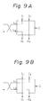
- FIGS 9A and 9B are views for explaining the connection configurations of the switch box.
- Each switch box comprises two input terminals I1 and I2 , two output terminals O1 and O2 , two link terminals L1 and L2 , and a control terminal C. These connection configurations are switched by a control signal input to the control terminal C from the control unit 72.
- Two output terminals O1 and O2 are connected to the next corresponding input terminals I1 and I2 , and two output terminals O1 and O2 of the end switch box 68 are connected to the output links 36 and 37, respectively.
- the message is input from the input link 35 and stored in the buffer 69.
- the buffer 69 is divided into, for example, sixteen memory areas corresponding to all of the nodes, and sequentially stores the message from the processor.
- the control unit 72 generates one destination node designation based on the exclusive OR from the connection pattern and the own node designation held in the register, and the other destination node designation based on the bits inverted from the exclusive OR.
- Two destination nodes determined by the control unit 72 are input to the buffer 69 through the signal line 77.
- Two messages designated by the control signal are read out from the predetermined area and input to the switch box 65 through the signal lines 70 and 71.
- the connection pattern setting unit 43 receives the bit trains to be simultaneously transferred to each mode as the phase signal.
- the bit trains are supplied from the bit train generator 51 in the global controller 55 commonly provided in the hyper cube network.
- the bit trains for example, four-bits trains, are transferred to the controller 72 through the connection pattern setting unit 43.
- the bit train generator 51 generates different bit trains at constant time intervals set as being sufficient for transferring one message. In this case, the bit train generator 51 generates 2 n kinds of bit trains during one period.
- the control unit 72 generates the control signal to be input to each control terminal C of each switch box.
- Each switch box is changed by the control signal between two connection configurations shown in Figs. 9A and 9B. That is, when the connection pattern is "1", the connection configuration is shown by Fig. 9A, and when the connection pattern is "0", the connection configuration is shown by Fig. 9B. Accordingly, for example, when the connection pattern is "0110", the switch boxes 65 and 68 are set to the connection configuration shown in Fig. 9B, and the switch boxes 66 and 67 are set to the connection configuration shown in Fig. 9A.
- the first connection configuration shown in Fig. 9A is formed by connecting the first input terminal I1 and the first link terminal L1 , the second input terminal I2 and the second output terminal O2 , and the second link terminal L2 and the first output terminal O2.
- the second connection configuration shown in Fig. 9B is formed by connecting the first input terminal I1 and the first output terminal O1 , the second input terminal I2 and the first link terminal L1 , and the second link terminal L2 and the second output terminal O2 , respectively.
- Figure 10 is a view for explaining one example of the connection configuration of the communication path.
- connection pattern is "0110".
- Each of the boxes corresponds to the switch box 65 to 68 shown in Fig. 10.
- I1 and I2 are the input links and O1 and O2 are, the output links.
- the switch box takes the connection configuration shown by Fig. 9B, and when the connection pattern is "1", the switch box takes the connection configuration shown by Fig. 9A.
- the input link I1 of the node designated "0000” is connected to the node designated "0010” by both switch boxes 66 passing through the switch box 65 of the node designated "0000". Further, the node designated "0010” is connected to the node designated "0110” by both switch boxes 67, and connected to the output link O1 of the node designated "0110".
- the node designated "0000" is connected to the node designated "1001" through the switch box 65 of the node designated "0000", the switch boxes 65 to 68 of the node designated "0001", and the switch box 68 of the node designated "1001".
- the destination node designation "1001" is similar to the node designation inverted from the node designation "0110". Accordingly, it is possible to automatically designate two destination nodes in the present invention.
- Figure 11 is a schematic block diagram for explaining the relationship between the node and the interfaces to the processor.
- RIF denotes a reception memory interface
- TIF a transmission memory interface
- E an exclusive OR circuit
- OE an odd/even judgement circuit
- IV a bit inverter
- N a NOT circuit
- TB a transmission buffer
- RB a reception buffer
- FIG. 5 This figure corresponds to the first embodiment shown in Fig. 5; i.e., the switch unit 40 corresponds to the switch unit 40 in Fig. 5; two interfaces RIF, the interface TIF, and the memory correspond to the buffer 42 and the peripheral portions in Fig. 5; and the connection pattern setting unit, the register, the exclusive OR circuit and the odd/even judgement circuit correspond to the register, the control unit and the connection pattern setting unit shown in Fig. 5.
- the node includes two interfaces RIF and one interface TIF both connected to the address bus and the data bus of the processor.
- the interface TIF inputs the messages read out sequentially from the buffer TB to the switch unit 40 through the address and the data bus line.
- the interface RIF stores the messages read out from the switch unit to the buffer RB in the memory through the address and the data bus line.
- the buffer TB has, for example, sixteen entries corresponding to all of the nodes.
- the interface TIF comprises, for example, sixteen registers corresponding to all of the nodes, and each of the registers stores the start address of each entry in the buffer TB.
- the buffer RB has, for example, sixteen entries corresponding to all of the nodes.
- the interface RIF comprises, for example, sixteen registers corresponding to all of the nodes, and each of registers stores the start address of each entry in the buffer RB.
- connection pattern setting unit receives the bit train simultaneously transferred from the global controller to each mode as the phase signal, and inverts to the control signal of the switch unit.
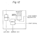
- FIG 12 is a detailed block diagram of the reception memory interface
- Figure 13 is a detailed block diagram of the transmission memory interface.
- the interfaces RIF and TIF are controlled by the phase signal from the global controller, and the control signal generated by the own node number from the register having the own node number.
- the interface RIF receives a node number designation signal and a start signal as the control signal.
- the direct memory access controller DMAC refers the entry of the buffer RB based on the address stored in the register corresponding to the node designated by the node number designation signal when the start of the reception is designated by the start signal, and stores the message, which is input from the output link of the switch unit to the FIFO, to the corresponding entry.
- the interface TIF receives the node number designation signal and the start signal as the control signal.
- the DMAC refers the entry of the buffer TB based on the address stored in the register corresponding to the node designated by the node number designation signal when the start of the transmission is designated by the start signal, and inputs the message stored in the corresponding entry to the FIFO.
- the transmission message input to the FIFO is output immedi strictlyately to the input link of the switch unit.
- the node number designation signal to the interface TIF is generated by calculating the exclusive OR between the phase signal and the own node number.
- the start signal to the interface TIF is always turned ON.
- the node number designation signal to the interface RIF (connected to the line 36) is generated by calculating the exclusive OR between the phase signal and the own node number.
- the node number designated signal to the interface RIF (connected to the line 37) is generated by calculating the exclusive OR between the inverted phase signal and the own node number.
- start signal to the interface RIF (connected to the line 36) is turned ON when the phase signal is even, and the start signal to the interface RIF (connected to the line 37) is turned ON when the phase signal is odd.
- Figure 14 is a schematic block diagram for explaining the relationship between the node and the interfaces to the processor. This figure corresponds to the second embodiment shown in Fig. 8. The same reference numbers shown in Fig. 11 are used for the same components of Fig. 14. S denotes the start signal generation circuit.
- the node includes two interfaces RIF and two interfaces TIF connected to the address bus and the data bus. Two input terminals of the first switch box are connected to the corresponding interfaces TIF. Two output terminals of the fourth switch box are connected to the corresponding interface RIF.
- the interface TIF reads out the message from the buffer TB, as in the first embodiment, and outputs the message to the corresponding input terminal.
- the interface RIF inputs the message from the corresponding output terminal, as in the first embodiment, and stores the message to the buffer RB.
- the transmission buffer TB and the reception buffer RB have the same structure as in the first embodiment.
- connection pattern setting unit receives the bit train, and transmits the control signal to control the connection configuration of each switch box in such a way that the switch box is set to the first connection configuration when the bit is "1", and set to the second connection configuration when the bit is "0".
- the node number designation signal to the interface TIF (connected to the line 70) is generated by calculating the exclusive OR between the phase signal and the own node number in the register, and the node number designation signal to the interface (connected to the line 71) is generated by calculating the inverted exclusive OR between the phase signal and the own node number.
- the node number designation signal to the interface RIF (connected to the line 36) is generated by calculating the exclusive OR between the phase signal and the own node number, and the node number designation signal to the interface RIF (connected to the line 37) is generated by calculating the inverted exclusive OR between the phase signal and the own node number.
- the start signal to the interfaces TIF and RIF are always turned ON. Further, the start signal generation cir cuit S is provided for detecting the start point of the phase signal from the global controller.
- Figure 15 is a graph for comparing the present invention and the previous proposal.
- CAP Cellular Array Processor
- the present invention is constituted by switch boxes of the CAP and the routing according to the present invention, and the comparison system is constituted by message passing by the CAP and the routing according to the previous proposal.
- the former is compared with the latter with regard to the transmission arrays and the reception arrays. That is, the elapsed time is measured between the time when each element of the transmission arrays is transferred to different destination nodes and the time when the messages from the different destination nodes are received by each element of the reception arrays.
- the lapsed time of the present invention is about ten times better than that of the previous proposal.
Landscapes
- Engineering & Computer Science (AREA)
- Computer Hardware Design (AREA)
- Physics & Mathematics (AREA)
- Theoretical Computer Science (AREA)
- Mathematical Physics (AREA)
- Software Systems (AREA)
- General Engineering & Computer Science (AREA)
- General Physics & Mathematics (AREA)
- Data Exchanges In Wide-Area Networks (AREA)
- Multi Processors (AREA)
Abstract
Description
- The present invention relates to a network control system in a hyper cube type network used in a multi-processors interconnection system.
- As is well known, the hyper cube type network is constituted by a plurality of nodes (2n nodes, n > 0, integer), each node being arranged on an apex of the cube, a plurality of links connecting the nodes, and a plurality of processors, each connected to each node.
- In general, two types of the multi-processors interconnection system are used, i.e., a multi-stage network and a multi-processors network.
- The multi-stage network includes various types of networks based on differences in the connection configuration thereof. For example, an omega network, a delta network, a banyan network, a shuffle-exchange network, etc. In general, these types, for example, the omega network and the shuffle-exchange network, have a plurality of switch boxes, and each switch box generally has two input terminals and two output terminals. Each switch box can take two connection configurations, i.e., cross and straight corresponding to a bit "1" and a bit "0". The switch boxes are connected by links from input stages to output stages in accordance with the above connection configurations, to form communication paths.
- In these types of network, however, although a high transfer speed can be achieved, a problem arises in that the number of communication paths which can be simultaneously used is limited, because the switch box can deal with only one communication path at a time.
- The multi-processor network is constituted by a plurality of nodes and links connected between the nodes, wherein each node has at least one buffer memory for temporarily storing input messages.
- This type of network is constituted by a ring type, tree type, hyper cube type, etc., in accordance with different arrangements of the nodes.
- In these types of network, however, a problem arises in that much time is required for writing/reading a message to and from the buffer memory, and thus transmission of a message is delayed in an all-to-all burst communication when many loads are connected to the network.
- The hyper cube type network can be obtained in both the multi-stage and the multi-processor type of network, in the connection configuration of the nodes and the links, by rewriting a topology thereof. That is, the network having the hyper cube topology exists in the multi-stage and multi-processor networks. In this case, it is possible to modify the shuffle-exchange network to the hyper cube topology by rewriting the structure thereof when the former does not have the hyper cube topology.
- It is desirable to achieve an improvement of the total processing performance of the processors connected to the hyper cube type network, particularly, in an all-to-all burst communication. The all-to-all burst communication is a communication pattern in which each processor can simultaneously communicate to all processors including oneself in the system. Therefore, in the present invention, all communication paths are previously scheduled to achieve an effective all-to-all burst communication in the hyper cube type network.
- One example of the multi-stage network is disclosed in, New Generation Computing, 1984, "A Multi Page-Memory Architecture and A Multiport Disk-Cache System", by Yuzuru Tanaka. This network is constituted by a plurality of ports, a plurality of memory banks, a plurality of switch boxes, and a controller. The controller controls the connection of switch boxes based on a predetermined control program. In this reference, however, the network is formed between the ports and the memory banks. Further, the topology of the network is the type of the shuffle-exchange network, and the switch box comprises two inputs and two outputs.
- When the network of this proposal is rewritten to the hyper cube topology, one half of the links are not used, and thus the process- ing performance is unsatisfactory.
- It is therefore desirable to provide a network control system in a hyper cube type network enabling a uniform access upon an all-to-all burst communication among all nodes without congestion and waiting at the links, by which the processing performance of the processor can be improved.
- In accordance with the present invention, there is provided a network control system in a hyper cube type network constituted by: 2n nodes (n > 0, integer), each node being arranged on an apex of a cube and having n sets of links for interconnecting other nodes to form an n-dimensional hyper cube type network; and a plurality of processors, each processor being connected to a said node by input/output links, thereby providing communication paths between processors through the nodes and links; each of the nodes comprising, a device for setting 2n different connection patterns corresponding to 2n phase signals, and a switching device for interconnecting between the links and between the input/output links in accordance with the connection patterns synchronized with the phase signals.
- Reference is made, by way of example, to the accompanying drawings in which:
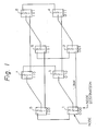
- Fig. 1 is a schematic diagram of one example of the structure of a three-dimensional hyper cube type network having eight nodes;
- Fig. 2 is a schematic block diagram of a previously proposed node;
- Fig. 3 is a basic structural view of a node according to the present invention;
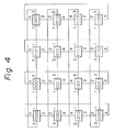
- Fig. 4 is one example of the connection of a four-dimensional hyper cube type network;
- Fig. 5 is a schematic block diagram of a node according to one embodiment of the present invention;
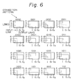
- Fig. 6 is a view for explaining the connection configuration of the switch unit corresponding to each connection pattern;
- Figs. 7A, 7B and 7C are views for explaining various communication paths corresponding to various connection patterns;
- Fig. 8 is a schematic block diagram of a node according to another embodiment of the present invention;
- Figs. 9A and 9B are views for explaining connection configurations of the switch box in Fig. 8;
- Fig. 10 is a view for explaining one example of the connection configuration of the communication path in the embodiment shown in Fig. 8;
- Fig. 11 is a schematic block diagram for explaining the relationship between the node and the interfaces to the processor with regard to the first embodiment shown in Fig. 5;
- Fig. 12 is a detailed block diagram of the reception memory interface shown in Fig. 11;
- Fig. 13 is a detailed block diagram of the transmission memory interface shown in Fig. 11;
- Fig. 14 is a schematic block diagram for explaining the relationship between the node and the interfaces to the processor regarding the second embodi- ment shown in Fig. 8; and
- Fig. 15 is a graph for comparing the present invention and a previous proposal.
- Before describing the preferred embodiments, an explanation will be given of a previously proposed hypercube type network.
- Figure 1 is a schematic diagram of one example of the structure of a three-dimensional (n = 3) hyper cube type network having eight (2³ = 8)
nodes 1 to 8. Each node is designated by binary numbers "000", "001" --- "111", has three links, and is connected to another node based on the following connection rule. For example, the first bit of the node designation of thenode 1 is different from that of thenode 2, and thus thelink 1 of thenode 1 is connected to thelink 1 of thenode 2. Further, the second bit of the node designation of thenode 1 is different from that of thenode 3, and accordingly, thelink 2 of thenode 1 is connected to thelink 2 of thenode 3. Still further, the third bit of the node designation of thenode 1 is different from that of thenode 5, and therefore, thelink 3 of thenode 1 is connected to thelink 3 of thenode 5. The same rule is applied to the other nodes, and thus all of the nodes are connected to each other in such a manner that they constitute a three-dimensional hyper cube type network. - In general, 2n nodes are distinguished by 2n node designations. Each of the node designations can be expressed by a binary number having n bits in the n-dimensional hyper cube type network. As is obvious from the above example, each node is connected to the other n nodes.
- Figure 2 is a schematic block diagram of a prior proposed node. This node is used in a multi-processors network.
- In Fig. 2,
reference number 10 denotes a reception control unit, 11 a transmission control unit, 12 an input control unit, 13 an output control unit, 14 a buffer memory, 15 a router, and 16 a bus line. - The
input control unit 12 and theoutput control unit 13 are connected to the processor (not shown), for controlling the reception or transmission of messages from or to the processor. Thereception control unit 10 and thetransmission control unit 11 are connected to the link for controlling the transmission and reception of messages from another node. Thebuffer memory 14 temporarily stores transmission and reception messages, and therouter 15 distinguishes an address of the message and controls another node to which it is to be relayed. - The
reception control unit 10 and theinput control unit 12 transfer messages input from the processor and the link, and thebuffer memory 14 stores the messages to the predetermined memory area. Thetransmission control unit 11 and theoutput control unit 13 transfer the messages read out from the memory area under the control of therouter 15. - The
router 15 comprises a suitable processing means for running a control program, and accordingly, based on the control program, therouter 15 distinguishes the node designation of the destination of the received message, determines the transmission destination to which it is to be relayed, and sends a command concerning the destination to thetransmission control unit 11 and theoutput control unit 13. - In each node, the message from the processor has the node designation of the destination at the head thereof, and the
input control unit 12 informs therouter 15 that the message has been stored. - The
router 15 compares the node designation of the destination of the received message stored in thebuffer memory 14 with the own node designation. If the former coincides with the latter, the destination of the received message is determined to be the own node. In this case, the received message is output to the processor connected to the own node through thetransmission control unit 11. - If the former does not coincide with the latter, the received message is output to another node having the number corresponding to the inconsistent bit of the former and the latter.
- For example, when the above node is applied to the hyper cube type network shown in Fig. 1, if the message is transmitted from the node 1 (000) to the node 6 (101) through the link (indicated by thick lines), the message from the processor connected to the
node 1 is temporarily stored in thebuffer memory 14 of thenode 1. Therouter 15 then compares the node designation "101" of thedestination node 6 with the own node designation "000" of thenode 1 and determines the link to be selected. In this case, since the first and the third bits of the node designation "000" and the node designation "101" are different, the link denoted by the thick line is selected. - Namely, when the
router 15 of thenode 1 selects the third link, the message is transferred from thebuffer memory 14 of thenode 1 to the third link through thetransmission control unit 11, and the message is stored in thebuffer memory 14 of thenode 5 through thereception control unit 10 therein. Therouter 15 of thenode 5 compares the node designation "101" of thedestination node 6 with the own node designation "100" of thenode 5, and determines the link to be selected. In this case, since the first bit is different in the node designation "101", the message is transferred from thebuffer memory 14 of thenode 5 to the first link through thetransmission control unit 11 therein. The message is stored in thebuffer memory 14 of thenode 6 through thereception control unit 10 therein, therouter 15 of thenode 6 distinguishes that the message designates the own node designation "101", and the message is then transferred to the processor connected to thenode 6 through theoutput control unit 13 therein. - As explained above, since the control of each node is independently performed, a plurality of messages can be transferred and processed in parallel in the hyper cube type network.
- Nevertheless, problems arise in this type of node when it is applied to the hyper cube type network and many messages to be processed exist in the network.
- First, the message quantities passing through each of the links are unbalanced so that a complex relation- ship of busy links and not-busy links exists in the network since it is not possible to make completely uniform the message quantities passing through each link.
- Accordingly, the rate of utilization of the link is reduced, and thus the total processing performance of the network is considerably lowered.
- Second, a router having a higher processing performance must be provided in each node, to process many messages passing through the link, and accordingly, the manufacturing cost per node is increased.
- A network control system according to the present invention will be explained in detail hereinafter.
- Figure 3 is a basic structural view of a node embodying the present invention. A plurality of nodes are connected to each other through links in such a manner that they form the hyper cube type network shown in Fig. 1.
- In Fig. 3,
reference number 20 denotes a node, 21 a switch unit, 22 links, 23 input links, 24 output links, 25 a connection pattern setting unit and 26 a phase signal. - Each
link 22 is connected to another node, and theinput link 23 and theoutput link 24 are connected to the processor. Theswitch unit 21 is connected to thelink 22, theinput link 23, and theoutput link 24, and switches the interconnection among these links in accordance with the connection pattern set by the settingunit 25 synchronized with thephase signal 26. - The
node 20 is one of 2n nodes, each having the same structure in the n-dimensional hyper cube type network, and eachnode 20 is connected by n sets oflinks 22 to the other n nodes. - The connection
pattern setting unit 25 determines 2n connection patterns synchronized with thephase signal 26. In this case, one period is constituted by 2n phases simultaneously supplied to all nodes. One phase signal contains n messages and can process 2n messages, and accordingly, the all-to-all burst communication is processed by 2n phases. - The
switch unit 21controls 2n kinds of connections during one period to interconnect thelink 22 and theinput link 23, and thelink 22 and theoutput link 24, based on the connection patterns supplied from theunit 25. - According to the above control, the busy state and waiting state of the link when relaying the message do not occur in the network without congestion of the message at the communication path, so that the processing performance of the network can be raised when performing an all-to-all burst communication.
- Figure 4 is one example of the connection of a four-dimensional hyper cube type network.
- Each of the nodes of the four-dimensional (n = 4) hyper cube type network is connected in accordance with the above mentioned connection rule. The binary number (0000, 0001 ---) at each node is the node designation, and the number at each line is the link number.
- Figure 5 is a schematic block diagram of a node according to one embodiment of the present invention.
- In Fig. 5,
reference number 30 denotes a node, 31 to 34 links, 35 an input link, 36 and 37 two output links, 39 an input line, 40 a switch unit, 41 a control unit, 42 a buffer memory, 43 a connection pattern setting unit, 44 a register, 50 a global controller, 51 a bit train generator, 52 a signal line, 53 an invertor, and 54 a signal line. - The
node 30 is connected to the links 31 to 34 and to the processor through theinput link 35 and twooutput links input link 35 is connected to theswitch unit 40 through thebuffer 42 and theinput line 39. The messages are temporarily stored in thebuffer 42 and sequentially read out from thebuffer 42 to theswitch unit 40 through theinput signal line 39. - The
buffer 42 has, for example, sixteen memory areas corresponding to the sixteen nodes shown in Fig. 4, and temporarily stores each message to be transferred from the processor to each node. - The
control unit 41 controls the connection configuration at theswitch unit 40 and selection of the message read out from thebuffer 42 based on the connection patterns supplied from the connectionpattern setting unit 43 and the own node designation held in theregister 44. - The connection
pattern setting unit 43 receives the bit train (here the bit train has four bits, since this embodiment concerns a four-dimensional (n = 4) network) of the phase signal simultaneously supplied from theglobal controller 50 to eachnode 30. This bit train is transferred to thecontrol unit 41 as a four-bits connection pattern. Theglobal controller 50 comprises thebit train generator 51 and theinvertor 53, and is provided in common in the hyper cube network. - The
bit train generator 51 generates different bit trains at constant time intervals set as being sufficient for transferring one message. This bit train is transferred to all nodes having an even node designation through thesignal line 52, and simultaneously, the bit train inverted by theinvertor 53 is transferred to all nodes having an odd node designation through thesignal line 54. Thebit train generator 51 can generate 2n kinds of bit trains during one period. - The even node designations are those containing zero or even numbers of the bit "1" in the bit train, and the odd node designations are those containing odd numbers of the bit "1" in the bit train; for example, the node designations "0000", "0101", "1111", etc., are even node designations, and the node designations "0001", "1011", etc., are odd designations. The
control unit 41 decodes the connection pattern from the con- nectionpattern setting unit 43 and generates the predetermined control signal. - The connection rule at the
switch unit 40 is briefly explained hereinafter. - The interconnection between the links and between the input/output links is performed in such a way that, each of bits from the first to n'th of the connection pattern is corresponded to each of links from the first to n'th, respectively, the input link is connected to the link corresponding to the most significant bit of the bit "1" contained in the connection pattern, the remaining bits "1" are paired from the upper bit and each pair of link is connected to corresponding each pair of bit, respectively, and the bits "0" contained in the connection pattern are paired from the upper bit and each pair of link is connected to corresponding each pair of bit, respectively; further, when the bit "1" does not exist in the connection pattern, the input link is connected to the
output link 36; when even numbers of the bit "1" exist in the connection pattern, the bit "1" of the least significant bit disconnected by the above connection manner is connected to theoutput link 36, then, when odd numbers of the bit "1" exist in the connection pattern, the bit "0" of the least significant bit disconnected by the above connection manner is connected to theoutput link 37. - Figure 6 is a view for explaining the connection configuration of the switch unit corresponding to each connection pattern.
- In Fig. 6,
reference numbers 1 to 4 denote links corresponding to links 31 to 34 in Fig. 5, "I" denotes an input line corresponding to theinput line 39, and "O₁" and "O₂" denote two output lines corresponding to theoutput lines - In this case, the
control unit 41 in Fig. 5 obtains an "exclusive OR" between the connection pattern and the own node designation of theregister 44, as the node designation of the destination, and transfers the exclusive OR as the control signal to thebuffer 42, where the message at the area assigned by the destination is read out from the buffer and transferred to theinput line 39. - For example, when the connection pattern is "0011", the node having an even node designation, for example, "1001", is connected to the node designated "1010", as shown by the thick lines in Fig. 4. The connection configuration of the connection pattern "0011" is shown in Fig. 6. The input line I is connected to the
first link 1 so that the input message is transferred to the node designated "1000" shown in Fig. 4. - In this case, since the node designation "1000" is for an odd node designation, the inverted connection pattern "1100" is used as the connection pattern. The connection pattern "1100" is shown in Fig. 6. That is, the
first link 1 is connected to thesecond link 2 so that the message input from thefirst link 1 is transferred to thesecond link 2 and further transferred to the node designated "1010". - In the node designation "1010", since this is an even node designation, again the connection pattern "0011" is used. The connection configuration of the connection pattern "0011" is shown in Fig. 6, as already explained. That is, the
second link 2 is connected to the output O₁. Accordingly, the message input from the processor of the node designated "1001" is transferred to the processor of the node designated "1010". - Figures 7A, 7B and 7C are views for explaining various communication paths in the hyper cube network. Fig. 7A shows the case where the connection pattern at the even node designation is "0010", Fig. 7B shows the case where the designation is "0101", and Fig. 7C shows the case where the designation is "1111". As obvious from the above, the connection patterns at the odd node designations are "1101", "1010", and "0000", respectively.
- In the above embodiment, the output links O₁ and O₂ are not used simultaneously because the dimension of the network is even (for example, n = 4). When the dimension is odd (for example, n = 3), both output lines O₁ and O₂ are used in a certain node and not used in the remaining nodes.
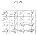
- Figure 8 is a schematic block diagram of the node according to another embodiment of the present invention.
- In Fig. 8,
reference number 60 denotes a node, 61a to 64b links, 65 to 68 switch boxes, 69 a buffer memory, 73 to 75 input signal lines, and 72 a control unit. Each of theswitch boxes 65 to 68 is connected to each of a pair of links 61a and 61b, 62a and 62b, 63a and 63b, and 64a and 64b. Theswitch box 65 is connected to twoinput links switch box 68 is connected to twooutput links - The interconnections between the links, and between the link and the input/output links are performed in such a way that, when the bit of the connection pattern is "1", the switch box is set to the first connection configuration, and when the bit of the connection pattern is "0", the switch box is set to the second connection configuration, as explained in detail hereinafter.
- Figures 9A and 9B are views for explaining the connection configurations of the switch box. Each switch box comprises two input terminals I₁ and I₂ , two output terminals O₁ and O₂ , two link terminals L₁ and L₂ , and a control terminal C. These connection configurations are switched by a control signal input to the control terminal C from the
control unit 72. Two output terminals O₁ and O₂ are connected to the next corresponding input terminals I₁ and I₂ , and two output terminals O₁ and O₂ of theend switch box 68 are connected to the output links 36 and 37, respectively. - The message is input from the
input link 35 and stored in the buffer 69. The buffer 69 is divided into, for example, sixteen memory areas corresponding to all of the nodes, and sequentially stores the message from the processor. - The
control unit 72 generates one destination node designation based on the exclusive OR from the connection pattern and the own node designation held in the register, and the other destination node designation based on the bits inverted from the exclusive OR. Two destination nodes determined by thecontrol unit 72 are input to the buffer 69 through the signal line 77. Two messages designated by the control signal are read out from the predetermined area and input to theswitch box 65 through thesignal lines - The connection
pattern setting unit 43 receives the bit trains to be simultaneously transferred to each mode as the phase signal. The bit trains are supplied from thebit train generator 51 in theglobal controller 55 commonly provided in the hyper cube network. The bit trains, for example, four-bits trains, are transferred to thecontroller 72 through the connectionpattern setting unit 43. - The
bit train generator 51 generates different bit trains at constant time intervals set as being sufficient for transferring one message. In this case, thebit train generator 51 generates 2n kinds of bit trains during one period. - The
control unit 72 generates the control signal to be input to each control terminal C of each switch box. Each switch box is changed by the control signal between two connection configurations shown in Figs. 9A and 9B. That is, when the connection pattern is "1", the connection configuration is shown by Fig. 9A, and when the connection pattern is "0", the connection configuration is shown by Fig. 9B. Accordingly, for example, when the connection pattern is "0110", theswitch boxes switch boxes - As explained above, the first connection configuration shown in Fig. 9A is formed by connecting the first input terminal I₁ and the first link terminal L₁ , the second input terminal I₂ and the second output terminal O₂ , and the second link terminal L₂ and the first output terminal O₂. The second connection configuration shown in Fig. 9B is formed by connecting the first input terminal I₁ and the first output terminal O₁ , the second input terminal I₂ and the first link terminal L₁ , and the second link terminal L₂ and the second output terminal O₂ , respectively.
- Figure 10 is a view for explaining one example of the connection configuration of the communication path.
- In Fig. 10, the connection pattern is "0110". Each of the boxes (dotted line) corresponds to the
switch box 65 to 68 shown in Fig. 10. Further, I₁ and I₂ are the input links and O₁ and O₂ are, the output links. As is obvious, when the connection pattern is "0", the switch box takes the connection configuration shown by Fig. 9B, and when the connection pattern is "1", the switch box takes the connection configuration shown by Fig. 9A. - For example, as shown by the thick line, the input link I₁ of the node designated "0000" is connected to the node designated "0010" by both
switch boxes 66 passing through theswitch box 65 of the node designated "0000". Further, the node designated "0010" is connected to the node designated "0110" by bothswitch boxes 67, and connected to the output link O₁ of the node designated "0110". - In case of the input link I₂ of the node designated "0000", as shown by another thick line, the node designated "0000" is connected to the node designated "1001" through the
switch box 65 of the node designated "0000", theswitch boxes 65 to 68 of the node designated "0001", and theswitch box 68 of the node designated "1001". - As is obvious, the destination node designation "1001" is similar to the node designation inverted from the node designation "0110". Accordingly, it is possible to automatically designate two destination nodes in the present invention.
- Figure 11 is a schematic block diagram for explaining the relationship between the node and the interfaces to the processor.
- In Fig. 11, RIF denotes a reception memory interface, TIF a transmission memory interface, E an exclusive OR circuit, OE an odd/even judgement circuit, IV a bit inverter, N a NOT circuit, TB a transmission buffer, and RB a reception buffer.
- This figure corresponds to the first embodiment shown in Fig. 5; i.e., the
switch unit 40 corresponds to theswitch unit 40 in Fig. 5; two interfaces RIF, the interface TIF, and the memory correspond to thebuffer 42 and the peripheral portions in Fig. 5; and the connection pattern setting unit, the register, the exclusive OR circuit and the odd/even judgement circuit correspond to the register, the control unit and the connection pattern setting unit shown in Fig. 5. - The node includes two interfaces RIF and one interface TIF both connected to the address bus and the data bus of the processor.
- The interface TIF inputs the messages read out sequentially from the buffer TB to the
switch unit 40 through the address and the data bus line. The interface RIF stores the messages read out from the switch unit to the buffer RB in the memory through the address and the data bus line. - The buffer TB has, for example, sixteen entries corresponding to all of the nodes. The interface TIF comprises, for example, sixteen registers corresponding to all of the nodes, and each of the registers stores the start address of each entry in the buffer TB. Similarly, the buffer RB has, for example, sixteen entries corresponding to all of the nodes. The interface RIF comprises, for example, sixteen registers corresponding to all of the nodes, and each of registers stores the start address of each entry in the buffer RB.
- The interconnections between links are controlled by the control signal received from the connection pattern setting unit. As mentioned above, the connection pattern setting unit receives the bit train simultaneously transferred from the global controller to each mode as the phase signal, and inverts to the control signal of the switch unit.
- Figure 12 is a detailed block diagram of the reception memory interface, and Figure 13 is a detailed block diagram of the transmission memory interface. The interfaces RIF and TIF are controlled by the phase signal from the global controller, and the control signal generated by the own node number from the register having the own node number.
- The interface RIF receives a node number designation signal and a start signal as the control signal. The direct memory access controller DMAC refers the entry of the buffer RB based on the address stored in the register corresponding to the node designated by the node number designation signal when the start of the reception is designated by the start signal, and stores the message, which is input from the output link of the switch unit to the FIFO, to the corresponding entry.
- The interface TIF receives the node number designation signal and the start signal as the control signal. The DMAC refers the entry of the buffer TB based on the address stored in the register corresponding to the node designated by the node number designation signal when the start of the transmission is designated by the start signal, and inputs the message stored in the corresponding entry to the FIFO. The transmission message input to the FIFO is output immediately to the input link of the switch unit.
- The node number designation signal to the interface TIF is generated by calculating the exclusive OR between the phase signal and the own node number. The start signal to the interface TIF is always turned ON. The node number designation signal to the interface RIF (connected to the line 36) is generated by calculating the exclusive OR between the phase signal and the own node number. The node number designated signal to the interface RIF (connected to the line 37) is generated by calculating the exclusive OR between the inverted phase signal and the own node number.
- Further, the start signal to the interface RIF (connected to the line 36) is turned ON when the phase signal is even, and the start signal to the interface RIF (connected to the line 37) is turned ON when the phase signal is odd.
- Figure 14 is a schematic block diagram for explaining the relationship between the node and the interfaces to the processor. This figure corresponds to the second embodiment shown in Fig. 8. The same reference numbers shown in Fig. 11 are used for the same components of Fig. 14. S denotes the start signal generation circuit.
- The node includes two interfaces RIF and two interfaces TIF connected to the address bus and the data bus. Two input terminals of the first switch box are connected to the corresponding interfaces TIF. Two output terminals of the fourth switch box are connected to the corresponding interface RIF. The interface TIF reads out the message from the buffer TB, as in the first embodiment, and outputs the message to the corresponding input terminal. The interface RIF inputs the message from the corresponding output terminal, as in the first embodiment, and stores the message to the buffer RB. The transmission buffer TB and the reception buffer RB have the same structure as in the first embodiment.
- The interconnection of each switch box is controlled by the control signal from the connection pattern setting unit. The connection pattern setting unit receives the bit train, and transmits the control signal to control the connection configuration of each switch box in such a way that the switch box is set to the first connection configuration when the bit is "1", and set to the second connection configuration when the bit is "0".
- The node number designation signal to the interface TIF (connected to the line 70) is generated by calculating the exclusive OR between the phase signal and the own node number in the register, and the node number designation signal to the interface (connected to the line 71) is generated by calculating the inverted exclusive OR between the phase signal and the own node number.
- The node number designation signal to the interface RIF (connected to the line 36) is generated by calculating the exclusive OR between the phase signal and the own node number, and the node number designation signal to the interface RIF (connected to the line 37) is generated by calculating the inverted exclusive OR between the phase signal and the own node number. The start signal to the interfaces TIF and RIF are always turned ON. Further, the start signal generation cir cuit S is provided for detecting the start point of the phase signal from the global controller.
- Figure 15 is a graph for comparing the present invention and the previous proposal.
- In Fig. 15, the ordinate denotes an elapsed time (msec), and the abscissa denotes a packet length (Kbyte). A CAP (Cellar Array Processor), multi-processor system developed by Fujitsu Laboratories Ltd. and constituted by sixty-four processors, is used in the experiment, and accordingly, the present invention is constituted by switch boxes of the CAP and the routing according to the present invention, and the comparison system is constituted by message passing by the CAP and the routing according to the previous proposal.
- Therefore, the former is compared with the latter with regard to the transmission arrays and the reception arrays. That is, the elapsed time is measured between the time when each element of the transmission arrays is transferred to different destination nodes and the time when the messages from the different destination nodes are received by each element of the reception arrays.
- As is clear from the graph, the lapsed time of the present invention is about ten times better than that of the previous proposal.
- In embodiments of the present invention, it is possible to uniformly perform an all-to-all burst communication among all nodes without congestion and waiting of the links in the hyper cube network. Further, in the second embodiment shown in Fig. 8, it is possible to reduce the processing time to a half of that of the first embodiment since two sets of all-to-all burst can be processed during one period in the second embodiment.
Claims (4)
means for setting 2n different connection patterns corresponding to 2n phase signals, and
switching means for interconnecting between said links and between said input/output links in accordance with said connection patterns synchronized with said phase signals.
said n dimensional hyper cube network is constituted in such a form that two nodes, at which only any one bit of said bit train of one node designation is different from a bit train of another node designation, are interconnected by one link;
said input/output links of each of said nodes comprising one input link and two output links;
each of said connection patterns is applied by a bit train having n bits corresponding to n links, and is applied in such a way that the connection pattern of one node including zero or even numbers of the bit "1" in the node designation is determined by a bit train inverted from all bits of the connection pattern of the other node including odd numbers of the bit "1" in the node designation; and
said interconnection between said links and between said input/output links is performed in such a way that, each of bits from the first to n'th of the connection pattern is corresponded to each of links from the first to n'th, respectively, the input link is connected to the link corresponding to the most significant bit of the bit "1" contained in the connection pattern, the remaining bits "1" are paired from the upper bit and each pair of link is connected to corresponding each pair of bit, respectively, and the bits "0" contained in the connection pattern are paired from the upper bit and each pair of link is connected to corresponding each pair of bit, respectively; further, when the bit "1" does not exist in the connection pattern, the input link is connected to the output link 36; when even numbers of the bit "1" exist in the connection pattern, the bit "1" of the least significant bit disconnected by the above connection manner is connected to the output link 36, then, when odd numbers of the bit "1" exist in the connection pattern, the bit "0" of the least significant bit disconnected by the above connection manner is connected to the output link 37.
said n dimensional hyper cube network is constituted in such a form that two nodes, at which only one bit of said bit train of one node designation is different from the bit train of another node designation, are interconnected by one link;
said input/output links of each of said nodes have two input links and two output links;
each of said connection patterns is applied by a bit train having n bits corresponding to n links;
said switching means comprises n switch boxes, each of said switch boxes having a first and a second input terminals, a first and a second output terminals, a first and a second link terminals, and control terminal; each of said switch boxes being set to a first connection configuration and a second connection configuration; each of said switch boxes being interconnected in series by connecting the first and the second output terminal to the first and the second input terminal of the next switch box, respectively; and each of said switch boxes corresponding to each bit of the connection pattern;
each input terminal at one end of said switch boxes is connected to each of the input links; each output terminal of the other end of said switch boxes is connected to each of the output links; the first link terminal is connected to the second link terminal of other node, and the second link terminal is connected to the first link terminal of other node; and
the interconnections between the links, and between the link and the input/output links are performed in such a way that, when the bit of the connection pattern is "1", the switch box is set to the first connection configuration, and when the bit of the connection pattern is "0", the switch box is set to the second connection configuration.
Applications Claiming Priority (2)
| Application Number | Priority Date | Filing Date | Title |
|---|---|---|---|
| JP205416/87 | 1987-08-19 | ||
| JP62205416A JP2509947B2 (en) | 1987-08-19 | 1987-08-19 | Network control system |
Publications (3)
| Publication Number | Publication Date |
|---|---|
| EP0304285A2 true EP0304285A2 (en) | 1989-02-22 |
| EP0304285A3 EP0304285A3 (en) | 1989-08-09 |
| EP0304285B1 EP0304285B1 (en) | 1993-10-20 |
Family
ID=16506487
Family Applications (1)
| Application Number | Title | Priority Date | Filing Date |
|---|---|---|---|
| EP88307621A Expired - Lifetime EP0304285B1 (en) | 1987-08-19 | 1988-08-17 | Network control system |
Country Status (4)
| Country | Link |
|---|---|
| US (1) | US5420982A (en) |
| EP (1) | EP0304285B1 (en) |
| JP (1) | JP2509947B2 (en) |
| DE (1) | DE3885041T2 (en) |
Cited By (2)
| Publication number | Priority date | Publication date | Assignee | Title |
|---|---|---|---|---|
| EP0389246A2 (en) * | 1989-03-20 | 1990-09-26 | Fujitsu Limited | A system for controlling communication between parallel computers |
| GB2251320A (en) * | 1990-12-20 | 1992-07-01 | Motorola Ltd | Parallel processor |
Families Citing this family (9)
| Publication number | Priority date | Publication date | Assignee | Title |
|---|---|---|---|---|
| US5794059A (en) | 1990-11-13 | 1998-08-11 | International Business Machines Corporation | N-dimensional modified hypercube |
| US5717947A (en) * | 1993-03-31 | 1998-02-10 | Motorola, Inc. | Data processing system and method thereof |
| JPH06290158A (en) * | 1993-03-31 | 1994-10-18 | Fujitsu Ltd | Reconstructible torus network system |
| JP3251138B2 (en) * | 1994-10-31 | 2002-01-28 | 富士通株式会社 | Hash method |
| US5996020A (en) * | 1995-07-21 | 1999-11-30 | National Security Agency | Multiple level minimum logic network |
| KR100208949B1 (en) * | 1996-10-14 | 1999-07-15 | 윤종용 | The augmented ring-banyan network and the self-routing method therof |
| US6182185B1 (en) * | 1998-11-23 | 2001-01-30 | Adc Telecommunications, Inc. | Port switches |
| KR100349671B1 (en) * | 1999-12-13 | 2002-08-22 | 한국전자통신연구원 | Apparatus And Method For Interconnecting 3-link Nodes, And Parallel Processing System Using Them |
| CN105205032B (en) * | 2015-08-25 | 2018-06-26 | 华为技术有限公司 | CPU interconnection means, system and its control method, control device |
Citations (4)
| Publication number | Priority date | Publication date | Assignee | Title |
|---|---|---|---|---|
| US4195344A (en) * | 1977-04-08 | 1980-03-25 | The President Of The Agency Of Industrial Science And Technology | Computer system with a configuration monitor |
| US4270170A (en) * | 1978-05-03 | 1981-05-26 | International Computers Limited | Array processor |
| EP0187994A2 (en) * | 1984-12-20 | 1986-07-23 | State University of New York | Topologically-distributed-memory multiprocessor computer and method of electronic computation using said computer |
| WO1987001485A1 (en) * | 1985-08-30 | 1987-03-12 | The University Of Southampton | A data processing device |
Family Cites Families (21)
| Publication number | Priority date | Publication date | Assignee | Title |
|---|---|---|---|---|
| US3312943A (en) * | 1963-02-28 | 1967-04-04 | Westinghouse Electric Corp | Computer organization |
| US3296426A (en) * | 1963-07-05 | 1967-01-03 | Westinghouse Electric Corp | Computing device |
| US3308436A (en) * | 1963-08-05 | 1967-03-07 | Westinghouse Electric Corp | Parallel computer system control |
| US3364472A (en) * | 1964-03-06 | 1968-01-16 | Westinghouse Electric Corp | Computation unit |
| US3815095A (en) * | 1972-08-29 | 1974-06-04 | Texas Instruments Inc | General-purpose array processor |
| JPS57121746A (en) * | 1981-01-22 | 1982-07-29 | Nec Corp | Information processing device |
| US4470114A (en) * | 1982-03-01 | 1984-09-04 | Burroughs Corporation | High speed interconnection network for a cluster of processors |
| US4709327A (en) * | 1983-05-31 | 1987-11-24 | Hillis W Daniel | Parallel processor/memory circuit |
| IT1206331B (en) * | 1983-10-25 | 1989-04-14 | Honeywell Inf Systems | DATA PROCESSING SYSTEM ARCHITECTURE. |
| US4805091A (en) * | 1985-06-04 | 1989-02-14 | Thinking Machines Corporation | Method and apparatus for interconnecting processors in a hyper-dimensional array |
| US5047917A (en) * | 1985-07-12 | 1991-09-10 | The California Institute Of Technology | Apparatus for intrasystem communications within a binary n-cube including buffer lock bit |
| US4739476A (en) * | 1985-08-01 | 1988-04-19 | General Electric Company | Local interconnection scheme for parallel processing architectures |
| US4814980A (en) * | 1986-04-01 | 1989-03-21 | California Institute Of Technology | Concurrent hypercube system with improved message passing |
| US4870568A (en) * | 1986-06-25 | 1989-09-26 | Thinking Machines Corporation | Method for searching a database system including parallel processors |
| US4819035A (en) * | 1986-09-11 | 1989-04-04 | Asahi Kogaku Kogyo Kabushiki Kaisha | Color separation optical reading apparatus |
| US4766534A (en) * | 1986-10-16 | 1988-08-23 | American Telephone And Telegraph Company, At&T Bell Laboratories | Parallel processing network and method |
| US4933933A (en) * | 1986-12-19 | 1990-06-12 | The California Institute Of Technology | Torus routing chip |
| US5058001A (en) * | 1987-03-05 | 1991-10-15 | International Business Machines Corporation | Two-dimensional array of processing elements for emulating a multi-dimensional network |
| US4891751A (en) * | 1987-03-27 | 1990-01-02 | Floating Point Systems, Inc. | Massively parallel vector processing computer |
| US4933936A (en) * | 1987-08-17 | 1990-06-12 | The United States Of America As Represented By The Administrator Of The National Aeronautics And Space Administration | Distributed computing system with dual independent communications paths between computers and employing split tokens |
| US4868818A (en) * | 1987-10-29 | 1989-09-19 | The United States Of America As Represented By The Administrator Of The National Aeronautics And Space Administration | Fault tolerant hypercube computer system architecture |
-
1987
- 1987-08-19 JP JP62205416A patent/JP2509947B2/en not_active Expired - Lifetime
-
1988
- 1988-08-17 EP EP88307621A patent/EP0304285B1/en not_active Expired - Lifetime
- 1988-08-17 DE DE88307621T patent/DE3885041T2/en not_active Expired - Fee Related
-
1993
- 1993-02-16 US US08/022,417 patent/US5420982A/en not_active Expired - Fee Related
Patent Citations (4)
| Publication number | Priority date | Publication date | Assignee | Title |
|---|---|---|---|---|
| US4195344A (en) * | 1977-04-08 | 1980-03-25 | The President Of The Agency Of Industrial Science And Technology | Computer system with a configuration monitor |
| US4270170A (en) * | 1978-05-03 | 1981-05-26 | International Computers Limited | Array processor |
| EP0187994A2 (en) * | 1984-12-20 | 1986-07-23 | State University of New York | Topologically-distributed-memory multiprocessor computer and method of electronic computation using said computer |
| WO1987001485A1 (en) * | 1985-08-30 | 1987-03-12 | The University Of Southampton | A data processing device |
Non-Patent Citations (1)
| Title |
|---|
| PROCEEDINGS OF THE 1980 INTERNATIONAL CONFERENCE ON PARALLEL PROCESSING, 26th-29th August 1980, pages 65-74, IEEE, New York, US; Y. CHOW et al.: "An international network for processor communication with optimized local connections" * |
Cited By (4)
| Publication number | Priority date | Publication date | Assignee | Title |
|---|---|---|---|---|
| EP0389246A2 (en) * | 1989-03-20 | 1990-09-26 | Fujitsu Limited | A system for controlling communication between parallel computers |
| EP0389246A3 (en) * | 1989-03-20 | 1992-05-13 | Fujitsu Limited | A system for controlling communication between parallel computers |
| US5157692A (en) * | 1989-03-20 | 1992-10-20 | Fujitsu Limited | System for controlling communication between parallel computers |
| GB2251320A (en) * | 1990-12-20 | 1992-07-01 | Motorola Ltd | Parallel processor |
Also Published As
| Publication number | Publication date |
|---|---|
| EP0304285A3 (en) | 1989-08-09 |
| EP0304285B1 (en) | 1993-10-20 |
| JP2509947B2 (en) | 1996-06-26 |
| JPS6449350A (en) | 1989-02-23 |
| DE3885041T2 (en) | 1994-02-10 |
| US5420982A (en) | 1995-05-30 |
| DE3885041D1 (en) | 1993-11-25 |
Similar Documents
| Publication | Publication Date | Title |
|---|---|---|
| EP0169208B1 (en) | Self-routing packet switching network | |
| EP0226632B1 (en) | A packet switching network with multiple packet destinations | |
| US4780873A (en) | Circuit switching network with routing nodes | |
| CA1248209A (en) | Reliable synchronous inter-node communication in a self-routing network | |
| US6314487B1 (en) | Adaptive routing controller of a crossbar core module used in a crossbar routing switch | |
| US4656622A (en) | Multiple paths in a self-routing packet and circuit switching network | |
| US4621359A (en) | Load balancing for packet switching nodes | |
| US4661947A (en) | Self-routing packet switching network with intrastage packet communication | |
| US4488288A (en) | End-to-end information memory arrangement in a line controller | |
| EP0198010B1 (en) | Packet switched multiport memory nxm switch node and processing method | |
| US5721819A (en) | Programmable, distributed network routing | |
| Duato et al. | Performance evaluation of adaptive routing algorithms for k-ary n-cubes | |
| PL135976B1 (en) | Distributed control digital switching system | |
| US5878227A (en) | System for performing deadlock free message transfer in cyclic multi-hop digital computer network using a number of buffers based on predetermined diameter | |
| EP0304285A2 (en) | Network control system | |
| JPS6340383B2 (en) | ||
| JPS6360579B2 (en) | ||
| JPH02228762A (en) | Parallel processing computer system | |
| EP0142332B1 (en) | Interconnection networks | |
| JPH04113444A (en) | Bidirectional ring bus device | |
| JP2976675B2 (en) | Array processor routing method | |
| JPS63257052A (en) | Multiprocessor system | |
| US20020110130A1 (en) | System for routing data packets through a crossbar switch in expansion mode | |
| Thurber | Computer communication techniques | |
| JP2679706B2 (en) | Self-routing control system |
Legal Events
| Date | Code | Title | Description |
|---|---|---|---|
| PUAI | Public reference made under article 153(3) epc to a published international application that has entered the european phase |
Free format text: ORIGINAL CODE: 0009012 |
|
| AK | Designated contracting states |
Kind code of ref document: A2 Designated state(s): DE FR GB |
|
| PUAL | Search report despatched |
Free format text: ORIGINAL CODE: 0009013 |
|
| AK | Designated contracting states |
Kind code of ref document: A3 Designated state(s): DE FR GB |
|
| 17P | Request for examination filed |
Effective date: 19891011 |
|
| 17Q | First examination report despatched |
Effective date: 19911018 |
|
| GRAA | (expected) grant |
Free format text: ORIGINAL CODE: 0009210 |
|
| AK | Designated contracting states |
Kind code of ref document: B1 Designated state(s): DE FR GB |
|
| REF | Corresponds to: |
Ref document number: 3885041 Country of ref document: DE Date of ref document: 19931125 |
|
| ET | Fr: translation filed | ||
| PLBE | No opposition filed within time limit |
Free format text: ORIGINAL CODE: 0009261 |
|
| STAA | Information on the status of an ep patent application or granted ep patent |
Free format text: STATUS: NO OPPOSITION FILED WITHIN TIME LIMIT |
|
| 26N | No opposition filed | ||
| PGFP | Annual fee paid to national office [announced via postgrant information from national office to epo] |
Ref country code: GB Payment date: 19980810 Year of fee payment: 11 |
|
| PGFP | Annual fee paid to national office [announced via postgrant information from national office to epo] |
Ref country code: FR Payment date: 19980814 Year of fee payment: 11 |
|
| PGFP | Annual fee paid to national office [announced via postgrant information from national office to epo] |
Ref country code: DE Payment date: 19980821 Year of fee payment: 11 |
|
| PG25 | Lapsed in a contracting state [announced via postgrant information from national office to epo] |
Ref country code: GB Free format text: LAPSE BECAUSE OF NON-PAYMENT OF DUE FEES Effective date: 19990817 |
|
| GBPC | Gb: european patent ceased through non-payment of renewal fee |
Effective date: 19990817 |
|
| PG25 | Lapsed in a contracting state [announced via postgrant information from national office to epo] |
Ref country code: FR Free format text: LAPSE BECAUSE OF NON-PAYMENT OF DUE FEES Effective date: 20000428 |
|
| PG25 | Lapsed in a contracting state [announced via postgrant information from national office to epo] |
Ref country code: DE Free format text: LAPSE BECAUSE OF NON-PAYMENT OF DUE FEES Effective date: 20000601 |
|
| REG | Reference to a national code |
Ref country code: FR Ref legal event code: ST |