EP0298002A1 - Transposition memory for a data processing circuit - Google Patents
Transposition memory for a data processing circuit Download PDFInfo
- Publication number
- EP0298002A1 EP0298002A1 EP88420230A EP88420230A EP0298002A1 EP 0298002 A1 EP0298002 A1 EP 0298002A1 EP 88420230 A EP88420230 A EP 88420230A EP 88420230 A EP88420230 A EP 88420230A EP 0298002 A1 EP0298002 A1 EP 0298002A1
- Authority
- EP
- European Patent Office
- Prior art keywords
- data
- memory
- register
- column
- input
- Prior art date
- Legal status (The legal status is an assumption and is not a legal conclusion. Google has not performed a legal analysis and makes no representation as to the accuracy of the status listed.)
- Granted
Links
Images


Classifications
-
- G—PHYSICS
- G06—COMPUTING; CALCULATING OR COUNTING
- G06F—ELECTRIC DIGITAL DATA PROCESSING
- G06F12/00—Accessing, addressing or allocating within memory systems or architectures
-
- G—PHYSICS
- G06—COMPUTING; CALCULATING OR COUNTING
- G06F—ELECTRIC DIGITAL DATA PROCESSING
- G06F7/00—Methods or arrangements for processing data by operating upon the order or content of the data handled
- G06F7/76—Arrangements for rearranging, permuting or selecting data according to predetermined rules, independently of the content of the data
- G06F7/78—Arrangements for rearranging, permuting or selecting data according to predetermined rules, independently of the content of the data for changing the order of data flow, e.g. matrix transposition or LIFO buffers; Overflow or underflow handling therefor
-
- G—PHYSICS
- G06—COMPUTING; CALCULATING OR COUNTING
- G06F—ELECTRIC DIGITAL DATA PROCESSING
- G06F17/00—Digital computing or data processing equipment or methods, specially adapted for specific functions
- G06F17/10—Complex mathematical operations
- G06F17/16—Matrix or vector computation, e.g. matrix-matrix or matrix-vector multiplication, matrix factorization
-
- G—PHYSICS
- G11—INFORMATION STORAGE
- G11C—STATIC STORES
- G11C19/00—Digital stores in which the information is moved stepwise, e.g. shift registers
- G11C19/28—Digital stores in which the information is moved stepwise, e.g. shift registers using semiconductor elements
Definitions
- the invention relates to integrated circuits for processing digital signals, and more particularly to those which carry out a weighted double summation, in line then in column, of digital values x (i, j) of a matrix of n x n digital values.
- each coefficient C i (v) represents a weighted summation of the values x (i, j) of line i assigned coefficients f (j, v);
- v represents a column index varying from O to n-1 and there are coefficients C i (v) for each row of index i. This operation is called row transformation.
- nxn signals representing the coefficients C i (v) From the nxn signals representing the coefficients C i (v), we produce nxn signals representing the coefficients C (u, v); each coefficient C (u, v) is a weighted summation of the values C i (v) of column v, assigned coefficients g (i, u); u represents a row index varying from O to n-1 and n coefficients C (u, v) are produced for each column with index v. This operation is the column transformation.
- This type of digital processing is encountered in particular for carrying out so-called cosine transformations where the coefficients f (j, v) and g (i, u) are of the form cos (2i + 1) u ⁇ / 2n; these transformations are useful for facilitating the compression of information in digital signal transmissions, and more particularly for digital image transmission.
- the integrated circuit architectures enabling this type of transformation to be carried out are relatively complex because they must allow processing in real time, that is to say that the digital data rate to be processed is imposed at the input of the circuit and the rate of data processed at the output must be as fast as the rate at the input.
- this bit rate is high and, for information, for digital image transmission, we want to be able to process a block of 16 x 16 digital values (256 image points) in less than 20 microseconds; successive blocks of 256 values occurring at the input of the circuit with a periodicity of the order of 20 microseconds.
- FIG. 1 represents in the form of a block diagram a fairly simple integrated circuit architecture that one can imagine for carrying out on a single integrated circuit chip the complete transformation of a block of nxn digital values x (i, j) into a block of nxn coefficients C (u, v).
- the whole is controlled by a SEQ sequencer.
- a block of nxn data x (i, j) to be processed is brought, by an input bus E, to the line transform operator CTL which produces nxn digital data representing nxn digital coefficients C i (v). These data are stored in the nxn addresses of the memory MEM 1 (memory of nxn words).
- the CTL circuit receives the successive values x (i, j) and performs the line transformation; but this time, the sequencer SEQ controls the switch AIG1 so as to store the results C i (v) in the second memory MEM 2.
- the data previously recorded in the memory MEM 1 are applied as digital values input to be processed, through the switch AIG2, to the CTC column transformation circuit which produces the coefficients C (u, v) at its output.
- a block of nxn coefficients C i (v) is stored in one of the memories while a block of coefficients C i (v) recorded in the previous period in the other memory is processed.
- This architecture is elegant but requires two memories capable of storing each nxn data C i (v). It must be clearly understood that in order to be able to perform a column transformation on the coefficients C i (v) all the coefficients C i (v) of the same column v must be stored. However, as these coefficients C i (v) arrive from the CTL circuit line by line, and not column by column, this means in practice that the column transformation can only start when all the coefficients C i (v) of the matrix are arrived from the CTL circuit. This is the reason why the architecture of figure 1 uses two memories operating alternately. In addition, it should be noted that if the data C i (v) are entered in a memory line by line (i being the line index), then they must be read in the following period column by column (v being the column index).
- the invention proposes a new transposition memory structure making it possible to receive data grouped line by line and to restore them grouped column by column; this memory makes it possible to replace the two memories of FIG. 1 and the switches between these memories and the operators CTC and CTL by a single memory block.
- this memory makes it possible not to use serial / parallel and parallel / serial converters in the case where the data is processed in the operators in serial or serial / parallel form.
- Each register is periodically filled with new data and emptied of the data previously contained; the period T corresponds to the frequency of introduction of new data into the memory.
- the first and second phases of memory operation that is to say the first and second phases of closing and opening of the switches and switching of the multiplexers, each last for a time nxT.
- This type of memory can be used with registers each storing several bits of data in parallel, including with registers each having as many storage cells in parallel as bits in each data.
- the memory can be used directly between two operators such as CTL and CTC if these operators work on data transmitted in the form of bits in parallel.
- the invention is particularly advantageous in the case where operators work on data transmitted both in series and in parallel (for example, the data is 16 bits each, transmitted over two wires in eight successive stages) where still data transmitted completely in series on a wire (for example data of 16 bits transmitted on a wire in 16 successive stages).
- the data is more generally in the form of m bits in parallel and p bits in series (that is to say that each data is transmitted on m conductors in p stages, the overall number of bits of each data being mxp)
- each shift register is constituted by m registers in parallel each receiving the bits of one of the m conductors, and the multiplexers also each comprise m first inputs, m second inputs and m outputs, each assigned to a particular conductor.
- the data processing circuit of FIG. 1 can then be replaced by a much simpler architecture in which the operator CTC is connected to the operator CTL by means of a single transposition memory according to the invention, and this even if the operators operate on data in series or partially in series.
- the network is represented in two configurations of connections corresponding to two successive operating phases each during a time nx T where T is the period of introduction of the successive data into the network.
- the phases are designated in the following by phase a and phase b respectively.
- the top of Figure 2 represents the first configuration, corresponding to the first phase (phase a).
- the bottom of the figure represents the second configuration, corresponding to the second phase (phase b).
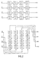
- the registers are designated by the references REG (i, j) where i is the number of the row and j the number of the column in which the register is located; thus, the first line comprises the registers REG (0,0), REG (0,1), REG (0,2), REG (0,3), the second line registers REG (1,0), REG ( 1.1), etc.
- the inputs E0 to E3 of the network are connected to the inputs of the various registers of the first column, and the outputs of the network, S0 to S3, are connected to the outputs of the registers of the last column.
- the entry of each register of columns other than the first is linked to the output of the register of the previous column on the same line.
- the data of the above matrix block are brought successively line by line on the inputs E0 to E3, that is to say that during a first period T, the inputs receive the four data of the first line, then, at the period following those of the second line, etc.
- the network contains all the data after a time equal to nx T, and this data is then presented according to the configuration below within the network of registers: C3 (0) C2 (0) C1 (0) C0 (0) C3 (1) C2 (1) C1 (1) C0 (1) C3 (2) C2 (2) C1 (2) C0 (2) C3 (3) C2 (3) C1 (3) C0 (3)
- a second phase b of operation also during a time nx T, the configuration of interconnections inside the network of registers changes and becomes that which is represented at the bottom of FIG. 2.
- the inputs E0, E1, E2, E3 are connected to the inputs of the registers of the last line, and the outputs S0, S1, S2, S3 are connected to the outputs of the registers of the first line.
- the entry of each register of lines other than the last is linked to the output of the register of the next line in the same column.
- the configuration of the data in the register network is as follows: C′0 (3) C′0 (2) C′0 (1) C′0 (0) C′1 (3) C′1 (2) C′1 (1) C′1 (0) C′2 (3) C′2 (2) C′2 (1) C′2 (0) C′3 (3) C′3 (2) C′3 (1) C′3 (0)
- the "prime" index indicates that this is a new data block.
- FIG. 2 is only a symbolic diagram of connections of the registers in the two alternate configurations of the network
- FIG. 3 shows the precise constitution of the network which makes it possible to achieve the operation described above.
- FIG. 3 shows some adjacent cells of the register network to show their interconnections.
- the elementary motif which is reproduced throughout the network is surrounded by a dashed line.
- the row index i varies from 0 to n-1 and the column index j varies from 0 to n-1 as well.
- Each register has an input and an output and it regularly stores, with a period T, a new datum which appears on its input.
- Each multiplexer has first and second inputs, and one output. It provides on its output the signal present on its first input during the first phase (phase a), and on the contrary the signal present on its second input during the second phase (phase b). It is therefore controlled by a logic signal with a period 2 n x T representing the two operating phases of the memory.
- the invention is particularly advantageous in cases b) and c).
- the pattern of connections which is repeated throughout the network is as follows: the first input of the MUX multiplexer (i, j) of the line i and of the column j is connected to the output REG register (i, j-1), that is to say the immediately lower column rank register on the same line i; the second input of the multiplexer is connected to the output of the REG register (i + 1, j), that is to say the following row rank register of the same column j.
- the output of the multiplexer is connected to the input of the REG register (i, j).
- FIG. 4 represents the connections between these first and last rows and columns and the inputs and outputs of the network.
- connections are made by switches actuated with the same frequency nx T as the multiplexers so that the network effectively changes from the configuration at the top of FIG. 2 to the configuration at the bottom of FIG. 2 with this same period. .
- the multiplexers of the first column all have their first input directly connected to a respective memory input: the first input of the MUX multiplexer (0,0) is connected to the E0 input, that of the multiplexer MUX (1.0) at input E1, that of the multiplexer MUX (nj-1.0) at input E (nj-1), etc.
- each register of the first line (of row 0 in line) is connected by a respective switch, open during the first phase a and closed during the second phase b, to a respective output of the memory: the output of the REG register (0,0) is connected by a switch to the output S (n-1); that of the REG register (0, j) is connected to the output S (nj-1); that of register REG (0, n-1) at output S0.
- each register in the last column (of rank n-1 in column) is connected by a respective switch, closed during the first phase a and open during the second phase b, to an output of the memory: the output of the register REG (0, n-1) is thus connected to the output S0, that of the REG register (1, n-1) to the output S1, etc.
- each multiplexer on the last line (of rank n-1 in line) is connected to a respective memory input: the second input of the MUX multiplexer (n-1.0) is connected to the input E (n-1), that of the MUX multiplexer (n-1, j) is connected to the input E (nj-1), that of the MUX multiplexer (n-1, n-1) is connected to the input E0.
- the second input of the multiplexer is the one which is connected to its output during phase b while the first input is connected to its output during phase a.
- the circuit thus described with reference to FIGS. 3 and 4 constitutes a single memory of nxn data into which a block of nxn data is entered line by line and into which the data is restored column by column at the same time as a new block of data is introduced line by line.
- K1 is substantially identical to the CLK signal; K2 is obtained simply by inverting CLK; Q1 is a signal having a transition to the low logic level after the transition from K1 to the high logic level and having a transition to the high level delayed with respect to the down transition from Q2; Q2 has, with respect to K2 and Q1, the same relation as Q1 with respect to K1 and Q2.
- Each stage of the elementary register of FIG. 6 is constituted as seen in the figure of a first transistor with N channel in series between the input of the stage and the input of an inverter; this transistor is controlled by the signal Q1 (Q2 for the second stage); the output of the inverter is looped back on the one hand to the gate of a P channel transistor inserted between a voltage source Vdd and the input of the inverter; on the other hand on the gate of an N channel transistor; the latter is in series between a ground terminal Vss and another N-channel transistor also connected to the input of the inverter and controlled by the signal K1 (or K2 for the second stage).
- FIG. 8 shows a circuit with nine inverters and two NOR gates making it possible to generate the signals K1, Q1, K2, Q2 from a clock signal CLK of symmetrical period T / p.
- FIG. 9 shows how a REG (i, j) register is produced from m x p elementary registers when the data comprises p bits in series on a bus of m conductors in parallel; each rectangle in FIG. 9 represents an elementary storage register of a bit, that is to say that a rectangle corresponds to the two-stage circuit of FIG. 6.
- the REG register (i, j) is entered by a bus of m conductors, each conductor arriving at the input of a set respective of p cascade elementary registers; there are am sets in parallel each corresponding to a conductor of the input bus; the output of the last register of each cascade assembly constitutes an output conductor of the REG register (i, j); the global output of the REG register (i, j) is a bus of m conductors constituted by the output conductors of the m assemblies in parallel.
- the multiplexers in this case comprise a first input constituted by a bus of m conductors, a second input constituted by a bus of m conductors, and an output constituted by a bus of m conductors, the output bus being connected to the bus of the first input during phase a and the second input bus during phase b.
Abstract
Description
L'invention concerne les circuits-intégrés de traitement de signaux numériques, et plus particulièrement ceux qui réalisent une double sommation pondérée, en ligne puis en colonne, de valeurs numériques x(i,j) d'une matrice de n x n valeurs numériques.The invention relates to integrated circuits for processing digital signals, and more particularly to those which carry out a weighted double summation, in line then in column, of digital values x (i, j) of a matrix of n x n digital values.
A partir des coefficients x(i,j) où i est un indice de ligne de la matrice, et j un indice de colonne, on cherche à produire une matrice de coefficients C(u,v) où u est un indice de ligne et v un indice de colonne, avec
A partir de signaux électriques d'entrée représentant les valeurs numériques x(i,j), on produit d'abord n x n signaux représentants des coefficients Ci(v) ; chaque coefficient Ci(v) représente une sommation pondérée des valeurs x(i,j) de la ligne i affectées de coefficients f(j,v) ; v représente un indice de colonne variant de O à n-1 et il y a n coefficients Ci(v) pour chaque ligne d'indice i. Cette opération est appelée transformation ligne. From electrical input signals representing the digital values x (i, j), first nxn signals representing coefficients C i (v) are produced; each coefficient C i (v) represents a weighted summation of the values x (i, j) of line i assigned coefficients f (j, v); v represents a column index varying from O to n-1 and there are coefficients C i (v) for each row of index i. This operation is called row transformation.
A partir des n x n signaux représentant les coefficients Ci(v), on produit n x n signaux représentant les coefficients C(u,v) ; chaque coefficient C(u,v) est une sommation pondérée des valeurs Ci(v) de la colonne v, affectées de coefficients g(i,u); u représente un indice de ligne variant de O à n-1 et on produit n coefficients C(u,v) pour chaque colonne d'indice v. Cette opération est la transformation colonne. From the nxn signals representing the coefficients C i (v), we produce nxn signals representing the coefficients C (u, v); each coefficient C (u, v) is a weighted summation of the values C i (v) of column v, assigned coefficients g (i, u); u represents a row index varying from O to n-1 and n coefficients C (u, v) are produced for each column with index v. This operation is the column transformation.
Ce type de traitement numérique se rencontre notamment pour réaliser des transformations dites transformations cosinus où les coefficients f(j,v) et g(i,u) sont de la forme cos (2i+1)u¶/2n ; ces transformations sont utiles pour faciliter la compression d'informations dans les transmissions numériques de signaux, et plus particulièrement pour la transmission numérique d'images.This type of digital processing is encountered in particular for carrying out so-called cosine transformations where the coefficients f (j, v) and g (i, u) are of the form cos (2i + 1) u¶ / 2n; these transformations are useful for facilitating the compression of information in digital signal transmissions, and more particularly for digital image transmission.
Les architectures de circuits intégrés permettant de réaliser ce type de transformation sont relativement complexes parce qu'elles doivent permettre un traitement en temps réel, c'est-à-dire que le débit de données numériques à traiter est imposé à l'entrée du circuit et le débit de données traitées à la sortie doit être aussi rapide que le débit à l'entrée. Bien entendu, ce débit est élevé et, à titre indicatif, pour la transmission numérique d'images, on veut pouvoir traiter un bloc de 16 x 16 valeurs numériques (256 points d'image) en moins de 20 microsecondes ; des blocs successifs de 256 valeurs se présentant à l'entrée du circuit avec une périodicité de l'ordre de 20 microsecondes.The integrated circuit architectures enabling this type of transformation to be carried out are relatively complex because they must allow processing in real time, that is to say that the digital data rate to be processed is imposed at the input of the circuit and the rate of data processed at the output must be as fast as the rate at the input. Of course, this bit rate is high and, for information, for digital image transmission, we want to be able to process a block of 16 x 16 digital values (256 image points) in less than 20 microseconds; successive blocks of 256 values occurring at the input of the circuit with a periodicity of the order of 20 microseconds.
La figure 1 représente sous forme de schéma-bloc une architecture de circuit intégré assez simple que l'on peut imaginer pour réaliser sur une même puce de circuit intégré la transformation complète d'un bloc de n x n valeurs numériques x(i,j) en un bloc de n x n coefficients C(u,v).FIG. 1 represents in the form of a block diagram a fairly simple integrated circuit architecture that one can imagine for carrying out on a single integrated circuit chip the complete transformation of a block of nxn digital values x (i, j) into a block of nxn coefficients C (u, v).
Dans ce schéma, on utilise un premier opérateur CTL exécutant la sommation en ligne, un deuxième opérateur CTC exécutant la sommation en colonne, deux mémoires MEM 1 et MEM 2 pour le stockage de valeurs représentant les coefficients Ci(v), et deux aiguillages AIG 1 et AIG 2 pour établir des chemins de connexion d'une part entre l'opérateur CTL et les mémoires MEM 1 et MEM 2 et d'autre part entre ces mémoires et l'opérateur CTC. L'ensemble est commandé par un séquenceur SEQ.In this diagram, one uses a first operator CTL executing the summation in line, a second operator CTC executing the summation in column, two
Un bloc de n x n données x(i,j) à traiter est amené, par un bus d'entrée E, à l'opérateur de transformée ligne CTL qui produit n x n données numériques représentant n x n coefficients numériques Ci(v). Ces données sont stockées dans les n x n adresses de la mémoire MEM 1 (mémoire de n x n mots). Le rythme de traitement des blocs de n x n données est par exemple de un bloc traité par 20 microsecondes ; une donnée x(i,j) se présente par exemple toutes les 74 nanosecondes (pour n x n = 256).A block of nxn data x (i, j) to be processed is brought, by an input bus E, to the line transform operator CTL which produces nxn digital data representing nxn digital coefficients C i (v). These data are stored in the nxn addresses of the memory MEM 1 (memory of nxn words). The processing rate of the blocks of nxn data is for example one block processed by 20 microseconds; a data x (i, j) occurs for example every 74 nanoseconds (for nxn = 256).
Pour le traitement du bloc suivant de n x n valeurs x(i,j), le circuit CTL reçoit les valeurs successives x(i,j) et effectue la transformation ligne ; mais cette fois, le séquenceur SEQ commande l'aiguillage AIG1 de manière à stocker les résultats Ci(v) dans la deuxième mémoire MEM 2. Pendant ce temps, les données précédemment enregistrées dans la mémoire MEM 1 sont appliquées à titre de valeurs numériques d'entrée à traiter, à travers l'aiguillage AIG2, au circuit de transformation colonne CTC qui produit à sa sortie les coefficients C(u,v).For the processing of the next block of nxn values x (i, j), the CTL circuit receives the successive values x (i, j) and performs the line transformation; but this time, the sequencer SEQ controls the switch AIG1 so as to store the results C i (v) in the
Ainsi de suite, alternativement, un bloc de n x n coefficients Ci(v) est stocké dans l'une des mémoires pendant qu'un bloc de coefficients Ci(v) enregistré à la période précédente dans l'autre mémoire est traité.So on, alternatively, a block of nxn coefficients C i (v) is stored in one of the memories while a block of coefficients C i (v) recorded in the previous period in the other memory is processed.
Cette architecture est élégante mais nécessite deux mémoires capables de stocker chacune n x n données Ci(v). Il faut bien comprendre en effet que pour pouvoir effectuer une transformation colonne sur les coefficients Ci(v) tous les coefficients Ci(v) d'une même colonne v doivent être mémorisées. Or, comme ces coefficients Ci(v) arrivent du circuit CTL ligne par ligne, et non colonne par colonne, cela veut dire en pratique que la transformation colonne ne peut commencer que lorsque tous les coefficients Ci(v) de la matrice sont arrivés du circuit CTL. C'est la raison pour laquelle l'architecture de la figure 1 utilise deux mémoires fonctionnant alternativement. De plus, il faut noter que si les données Ci(v) sont inscrites dans une mémoire ligne par ligne (i étant l'indice de ligne), alors elles doivent être lues à la période suivante colonne par colonne (v étant l'indice de colonne).This architecture is elegant but requires two memories capable of storing each nxn data C i (v). It must be clearly understood that in order to be able to perform a column transformation on the coefficients C i (v) all the coefficients C i (v) of the same column v must be stored. However, as these coefficients C i (v) arrive from the CTL circuit line by line, and not column by column, this means in practice that the column transformation can only start when all the coefficients C i (v) of the matrix are arrived from the CTL circuit. This is the reason why the architecture of figure 1 uses two memories operating alternately. In addition, it should be noted that if the data C i (v) are entered in a memory line by line (i being the line index), then they must be read in the following period column by column (v being the column index).
De plus, si cette architecture est utilisée avec des opérateurs CTC et CTL traitant des données numériques dont les bits sont transmis en série (ou partiellement en série) et non pas exclusivement en parallèle, alors il faut prévoir en plus entre les opérateurs et les mémoires des convertisseurs série/parallèle et parallèle/série car les mémoires classiques, SRAM ou DRAM ne peuvent traiter que des données dont les bits sont amenés sous forme parallèle. Pourtant il est souvent intéressant, dès que les données ont plus de 4 bits, de prévoir des opérateurs CTC et CTL travaillant sur des bits série ou série-parallèle.In addition, if this architecture is used with CTC and CTL operators processing digital data, the bits of which are transmitted in series (or partially in series) and not exclusively in parallel, then provision must also be made between operators and memories serial / parallel and parallel / serial converters because conventional memories, SRAM or DRAM can only process data whose bits are brought in parallel form. However, it is often interesting, as soon as the data has more than 4 bits, to provide CTC and CTL operators working on serial or serial-parallel bits.
L'invention propose une nouvelle structure de mémoire de transposition permettant de recevoir des données groupées ligne par ligne et de les restituer groupées colonne par colonne; cette mémoire permet de remplacer les deux mémoires de la figure 1 et les aiguillages entre ces mémoires et les opérateurs CTC et CTL par un seul bloc mémoire. De plus, cette mémoire permet de ne pas utiliser de convertisseurs série/parallèle et parallèle/série dans le cas où les données sont traitées dans les opérateurs sous forme série ou série/parallèle.The invention proposes a new transposition memory structure making it possible to receive data grouped line by line and to restore them grouped column by column; this memory makes it possible to replace the two memories of FIG. 1 and the switches between these memories and the operators CTC and CTL by a single memory block. In addition, this memory makes it possible not to use serial / parallel and parallel / serial converters in the case where the data is processed in the operators in serial or serial / parallel form.
La mémoire selon l'invention possède n entrées pour recevoir n données groupées ligne par ligne et n sorties pour restituer les données groupées colonne par colonne, les données étant les n x n données d'une matrice carrée de données et les données étant transmises et traitées sous forme de signaux électriques. La mémoire comporte un réseau de registres et de multiplexeurs, agencés en lignes et colonnes, chaque registre étant associé à un multiplexeur. Le registre au carrefour d'une ligne i et d'une colonne j étant désigné par REG(i,j) et le multiplexeur correspondant par MUX(i,j), le multiplexeur MUX(i,j) ayant une première entrée reliée à la sortie du registre REG(i,j-1), une deuxième entrée reliée à la sortie du registre REG(i+1,j), et une sortie reliée à l'entrée du registre REG(i,j), la sortie du multiplexeur transmettant l'état de la première entrée pendant une première phase de fonctionnement de la mémoire et transmettant l'état de la deuxième entrée pendant une deuxième phase. Pour les premières et dernières lignes et colonnes du réseau, les connexions sont les suivantes:
- a) les premières entrées des multiplexeurs de la première colonne (de rang 0) sont reliées chacune à une entrée respective de la mémoire;
- b) les sorties des registres de la dernière colonne (de rang n-1) sont reliées chacune par un interrupteur respectif à une sortie respective de la mémoire, cet interrupteur étant fermé pendant la première phase et ouvert pendant la deuxième phase;
- c) la sortie de chaque registre de la première ligne (de rang 0) est reliée, par un interrupteur ouvert pendant la première phase et fermé pendant la deuxième, à une sortie respective de la mémoire;
- d) la deuxième entrée de chaque multiplexeur de la dernière ligne (de rang n-1) est reliée à une entrée respective de la mémoire.
- a) the first inputs of the multiplexers of the first column (of rank 0) are each connected to a respective input of the memory;
- b) the outputs of the registers of the last column (of rank n-1) are each connected by a respective switch to a respective output of the memory, this switch being closed during the first phase and open during the second phase;
- c) the output of each register of the first line (of rank 0) is connected, by a switch open during the first phase and closed during the second, to a respective output of the memory;
- d) the second input of each multiplexer of the last line (of rank n-1) is connected to a respective input of the memory.
Chaque registre est périodiquement rempli d'une nouvelle donnée et vidé de la donnée précédemment contenue; la période T correspond à la fréquence d'introduction de nouvelles données dans la mémoire. La première et la deuxième phases de fonctionnement de la mémoire, c'est-à-dire la première et la deuxième phases de fermeture et d'ouverture des interrupteurs et de basculement des multiplexeurs, durent chacune un temps nxT.Each register is periodically filled with new data and emptied of the data previously contained; the period T corresponds to the frequency of introduction of new data into the memory. The first and second phases of memory operation, that is to say the first and second phases of closing and opening of the switches and switching of the multiplexers, each last for a time nxT.
Ce type de mémoire est utilisable avec des registres stockant chacun en parallèle plusieurs bits d'une donnée, y compris avec des registres ayant chacun autant de cases de stockage en parallèle que de bits dans chaque donnée. Dans ce cas, la mémoire est utilisable directement entre deux opérateurs tels que CTL et CTC si ces opérateurs travaillent sur des données transmises sous forme de bits en parallèle.This type of memory can be used with registers each storing several bits of data in parallel, including with registers each having as many storage cells in parallel as bits in each data. In this case, the memory can be used directly between two operators such as CTL and CTC if these operators work on data transmitted in the form of bits in parallel.
Mais l'invention est particulièrement avantageuse dans le cas où les opérateurs travaillent sur des données transmises à la fois en série et en parallèle (par exemple, les données sont de 16 bits chacune, transmises sur deux fils en huit étapes successives) où encore des données transmises complètement en série sur un fil (par exemple des données de 16 bits transmises sur un fil en 16 étapes successives).However, the invention is particularly advantageous in the case where operators work on data transmitted both in series and in parallel (for example, the data is 16 bits each, transmitted over two wires in eight successive stages) where still data transmitted completely in series on a wire (for example data of 16 bits transmitted on a wire in 16 successive stages).
Dans ce cas, chaque registre est un registre à décalage à plusieurs positions successives entre son entrée et sa sortie; le nombre de positions successives entre l'entrée et la sortie est égal au nombre p de bits série des données à traiter; le registre est actionné avec une période t = T/p. Si les données se présentent plus généralement sous forme de m bits en parallèle et p bits en série (c'est-à-dire que chaque donnée est transmise sur m conducteurs en p étapes, le nombre de bits global de chaque donnée étant m x p), alors, chaque registre à décalage est constitué par m registres en parallèle recevant chacun les bits de l'un des m conducteurs, et les multiplexeurs comportent aussi chacun m premières entrées, m deuxièmes entrées et m sorties, chacune affectée à un conducteur particulier.In this case, each register is a shift register with several successive positions between its input and its output; the number of successive positions between the input and the output is equal to the number p of serial bits of the data to be processed; the register is activated with a period t = T / p. If the data is more generally in the form of m bits in parallel and p bits in series (that is to say that each data is transmitted on m conductors in p stages, the overall number of bits of each data being mxp) , then, each shift register is constituted by m registers in parallel each receiving the bits of one of the m conductors, and the multiplexers also each comprise m first inputs, m second inputs and m outputs, each assigned to a particular conductor.
Le circuit de traitement de données de la figure 1 peut alors être remplacé par une architecture beaucoup plus simple dans laquelle l'opérateur CTC est relié à l'opérateur CTL par l'intermédiaire d'une seule mémoire de transposition selon l'invention, et ceci même si les opérateurs fonctionnent sur des données en série ou partiellement en série.The data processing circuit of FIG. 1 can then be replaced by a much simpler architecture in which the operator CTC is connected to the operator CTL by means of a single transposition memory according to the invention, and this even if the operators operate on data in series or partially in series.
D'autres caractéristiques et avantages de l'invention apparaîtront à la lecture de la description détaillée qui suit et qui est faite en référence aux dessins annexés dans lesquels:
- - la figure 1, déjà décrite représente une possibilité d'architecture de circuit exécutant une double sommation, en ligne puis en colonne, de valeurs numériques;
- - la figure 2 représente symboliquement le réseau de registres constituant la mémoire selon l'invention, avec deux configurations différentes de connexions entre les registres et les entrées et sorties de la mémoire;
- -la figure 3 représente un motif élémentaire du réseau de registres selon l'invention, avec les connexions entre registres voisins;
- - la figure 4 représente les interconnexions entre les entrées et sorties de la mémoire et les premières et dernières lignes et colonnes du réseau de registres;
- - la figure 5 représente un circuit de traitement de données utilisant une mémoire selon l'invention.
- - la figure 6 représente un registre élémentaire de stockage d'un bit unique de données;
- - la figure 7 représente le chronogramme des signaux de commande du registre élémentaire de la figure 6;
- - la figure 8 représente le circuit d'établissement des signaux de commande du registre élémentaire de la figure 6;
- - la figure 9 représente un registre REG(i,j) du réseau constituant la mémoire selon l'invention, ce registre étant constitué par m x p registres élémentaires de stockage d'un bit.
- - Figure 1, already described, represents a possibility of circuit architecture executing a double summation, in line then in column, of numerical values;
- FIG. 2 symbolically represents the network of registers constituting the memory according to the invention, with two different configurations of connections between the registers and the inputs and outputs of the memory;
- FIG. 3 represents an elementary pattern of the network of registers according to the invention, with the connections between neighboring registers;
- - Figure 4 shows the interconnections between the inputs and outputs of the memory and the first and last rows and columns of the register network;
- - Figure 5 shows a data processing circuit using a memory according to the invention.
- - Figure 6 shows an elementary storage register of a single bit of data;
- - Figure 7 shows the timing diagram of the control signals of the elementary register of Figure 6;
- FIG. 8 represents the circuit for establishing the control signals of the elementary register of FIG. 6;
- FIG. 9 represents a register REG (i, j) of the network constituting the memory according to the invention, this register being constituted by mxp elementary registers for storing a bit.
Pour mieux faire comprendre l'invention, on a représenté à la figure 2 un réseau simplifié de registres disposés en lignes et colonnes et destiné au stockage d'une matrice de n x n données numériques, avec n = 4. Le réseau est représenté dans deux configurations de connexions correspondant à deux phases de fonctionnement successives durant chacune un temps n x T où T est la période d'introduction des données successives dans le réseau. Les phases sont désignées dans ce qui suit par phase a et phase b respectivement.To make the invention easier to understand, FIG. 2 shows a simplified network of registers arranged in rows and columns and intended for the storage of a matrix of nxn digital data, with n = 4. The network is represented in two configurations of connections corresponding to two successive operating phases each during a time nx T where T is the period of introduction of the successive data into the network. The phases are designated in the following by phase a and phase b respectively.
Le haut de la figure 2 représente la première configuration, correspondant à la première phase (phase a). Le bas de la figure représente la deuxième configuration, correspondant à la deuxième phase (phase b).The top of Figure 2 represents the first configuration, corresponding to the first phase (phase a). The bottom of the figure represents the second configuration, corresponding to the second phase (phase b).
Le réseau comporte n entrées, E0, E1, E2, E3 et n sorties S0, S1, S2, S3. Il comporte n x n registres susceptibles de stocker chacun une donnée numérique d'une matrice de données n x n qui serait constituée comme ci-après pour n = 4:
Les registres sont désignés par les références REG(i,j) où i est le numéro de la ligne et j le numéro de la colonne dans lequel se situe le registre; ainsi, la première ligne comprend les registres REG(0,0), REG(0,1), REG(0,2), REG(0,3), la deuxième ligne les registres REG(1,0), REG(1,1), etc.The registers are designated by the references REG (i, j) where i is the number of the row and j the number of the column in which the register is located; thus, the first line comprises the registers REG (0,0), REG (0,1), REG (0,2), REG (0,3), the second line registers REG (1,0), REG ( 1.1), etc.
Dans la première phase a de fonctionnement, les entrées E0 à E3 du réseau sont reliées aux entrées des différents registres de la première colonne, et les sorties du réseau, S0 à S3, sont reliées aux sorties des registres de la dernière colonne. De plus, l'entrée de chaque registre des colonnes autres que la première est reliée à la sortie du registre de la colonne précédente sur la même ligne.In the first phase a of operation, the inputs E0 to E3 of the network are connected to the inputs of the various registers of the first column, and the outputs of the network, S0 to S3, are connected to the outputs of the registers of the last column. In addition, the entry of each register of columns other than the first is linked to the output of the register of the previous column on the same line.
Les données du bloc matriciel ci-dessus sont amenées successivement ligne par ligne sur les entrées E0 à E3, c'est-à-dire que pendant une première période T, les entrées reçoivent les quatre données de la première ligne, puis, à la période suivante celles de la deuxième ligne, etc.The data of the above matrix block are brought successively line by line on the inputs E0 to E3, that is to say that during a first period T, the inputs receive the four data of the first line, then, at the period following those of the second line, etc.
Le réseau contient toutes les données au bout d'un temps égal à n x T, et ces données se présentent alors selon la configuration ci-dessous à l'intérieur du réseau de registres:
Dans une deuxième phase b de fonctionnement, durant aussi un temps n x T, la configuration d'interconnexions à l'intérieur du réseau de registres change et devient celle qui est représentée au bas de la figure 2. Les entrées E0, E1, E2, E3 sont connectées aux entrées des registres de la dernière ligne, et les sorties S0, S1, S2, S3 sont connectées aux sorties des registres de la première ligne . De plus, l'entrée de chaque registre des lignes autres que la dernière est reliée à la sortie du registre de la ligne suivante dans la même colonne.In a second phase b of operation, also during a time nx T, the configuration of interconnections inside the network of registers changes and becomes that which is represented at the bottom of FIG. 2. The inputs E0, E1, E2, E3 are connected to the inputs of the registers of the last line, and the outputs S0, S1, S2, S3 are connected to the outputs of the registers of the first line. In addition, the entry of each register of lines other than the last is linked to the output of the register of the next line in the same column.
Par conséquent, pendant cette deuxième phase de n périodes T, le réseau de registres va d'une part se charger de nouvelles données (un autre bloc matriciel de n x n données), et d'autre part se décharger des données précédemment stockées.Consequently, during this second phase of n periods T, the network of registers will on the one hand take charge of new data (another matrix block of n x n data), and on the other hand unload data previously stored.
Mais le déchargement s'effectue à travers les registres de la première ligne et les données remontent progressivement des autres lignes vers la première ligne, de sorte que les données qui sortent sont d'abord les données suivantes:
Autrement dit, alors qu'on avait introduit les données du bloc matriciel ligne par ligne pendant la première phase, on les ressort colonne par colonne.In other words, when we had entered the data of the matrix block line by line during the first phase, we bring them out column by column.
De même, pendant cette deuxième phase, on introduit à nouveau des données ligne par ligne comme précédemment, mais elles arrivent par la dernière ligne du réseau de registres et remontent progressivement "verticalement" d'une ligne à la précédente (alors que dans la première phase elles se déplaçaient "horizontalement" d'une colonne à la suivante).Likewise, during this second phase, data is again introduced line by line as before, but they arrive via the last line of the network of registers and progressively go up "vertically" from one line to the previous one (whereas in the first phase they moved "horizontally" from one column to the next).
Il en résulte qu'à la fin de la deuxième phase, la configuration des données dans le réseau de registres est la suivante:
L'indice "prime" indique qu'il s'agit d'un nouveau bloc de données.The "prime" index indicates that this is a new data block.
On recommence alors une première phase a, c'est-à-dire qu'on repasse dans la configuration de connexions du haut de la figure 2 et on sort les données horizontalement; les premières données qui sortent sont donc les suivantes:
Autrement dit, là encore, les données qui ont été introduites ligne par ligne lors de la deuxième phase sont restituées colonne par colonne lors d'une nouvelle première phase.In other words, here again, the data which were entered line by line during the second phase are restored column by column during a new first phase.
Alors que la figure 2 n'est qu'un schéma symbolique de connexions des registres dans les deux configurations alternées du réseau, la figure 3 montre la constitution précise du réseau qui permet d'aboutir au fonctionnement décrit ci-dessus.While FIG. 2 is only a symbolic diagram of connections of the registers in the two alternate configurations of the network, FIG. 3 shows the precise constitution of the network which makes it possible to achieve the operation described above.
On a représenté sur la figure 3 quelques cellules adjacentes du réseau de registres pour montrer leurs interconnexions. Le motif élémentaire qui se reproduit dans tout le réseau, est entouré d'un trait tireté.FIG. 3 shows some adjacent cells of the register network to show their interconnections. The elementary motif which is reproduced throughout the network is surrounded by a dashed line.
A chaque registre REG(i,j) correspondant à la ième ligne et a la jème colonne, est associé un multiplexeur MUX(i,j).Each REG register (i, j) corresponding to the i th row and to the j th column, is associated with a multiplexer MUX (i, j).
L'indice de ligne i varie de 0 à n-1 et l'indice de colonne j varie de 0 à n-1 également.The row index i varies from 0 to n-1 and the column index j varies from 0 to n-1 as well.
Chaque registre comporte une entrée et une sortie et il stocke régulièrement, avec une période T, une nouvelle donnée qui se présente sur son entrée.Each register has an input and an output and it regularly stores, with a period T, a new datum which appears on its input.
Chaque multiplexeur comporte une première et une deuxième entrée, et une sortie. Il fournit sur sa sortie le signal présent sur sa première entrée pendant la première phase (phase a), et au contraire le signal présent sur sa deuxième entrée pendant la deuxième phase (phase b). Il est donc commandé par un signal logique de période 2 n x T représentant les deux phases de fonctionnement de la mémoire.Each multiplexer has first and second inputs, and one output. It provides on its output the signal present on its first input during the first phase (phase a), and on the contrary the signal present on its second input during the second phase (phase b). It is therefore controlled by a logic signal with a
On donnera plus loin des exemples de réalisation de registres et multiplexeurs, mais on peut déjà dire que leur constitution dépend du type de données qui sont reçues:
- a) si les données sont fournies sous forme de m bits en parallèle, les entrées et sorties des registres et des multiplexeurs sont des bus de m conducteurs; les registres possèdent chacun m cases en parallèle.
- b) si les données sont fournies sous forme de p bits en série, les entrées et sorties comportent à chaque fois un seul conducteur transmettant ces bits à un rythme régulier de période t = T/p; le registre est un registre à décalage à p positions successives, actionné à la période t = T/p, et chaque bit de donnée introduit à l'entrée d'un registre se retrouve à la sortie au bout du temps T.
- c) si les données sont traitées d'une manière mixte, série/parallèle, la structure est mixte: si les données comportent p bits en série sur chacun de m conducteurs, les entrées et sorties des registres et multiplexeurs sont des bus de m conducteurs, et les registres sont des ensembles de m registres à décalage travaillant en parallèle, chaque registre à décalage ayant p positions successives et étant actionné à la période t = T/p.
- a) if the data are supplied in the form of m bits in parallel, the inputs and outputs of the registers and of the multiplexers are buses of m conductors; the registers each have m boxes in parallel.
- b) if the data are supplied in the form of p bits in series, the inputs and outputs each time comprise a single conductor transmitting these bits at a regular rate of period t = T / p; the register is a shift register with p successive positions, actuated at the period t = T / p, and each bit of data introduced at the input of a register is found at the output at the end of time T.
- c) if the data is processed in a mixed manner, serial / parallel, the structure is mixed: if the data comprises p bits in series on each of m conductors, the inputs and outputs of the registers and multiplexers are buses of m conductors , and the registers are sets of m shift registers working in parallel, each shift register having p successive positions and being actuated at the period t = T / p.
L'invention s'avère particulièrement intéressante dans les cas b) et c).The invention is particularly advantageous in cases b) and c).
Pour revenir à la figure 3, on voit que le motif de connexions qui se répète sur tout le réseau est le suivant: la première entrée du multiplexeur MUX(i,j) de la ligne i et de la colonne j est reliée à la sortie du registre REG(i,j-1), c'est-à-dire le registre de rang de colonne immédiatement inférieur sur la même ligne i; la deuxième entrée du multiplexeur est reliée à la sortie du registre REG(i+1,j), c'est-à-dire le registre de rang de ligne suivant de la même colonne j.To return to FIG. 3, it can be seen that the pattern of connections which is repeated throughout the network is as follows: the first input of the MUX multiplexer (i, j) of the line i and of the column j is connected to the output REG register (i, j-1), that is to say the immediately lower column rank register on the same line i; the second input of the multiplexer is connected to the output of the REG register (i + 1, j), that is to say the following row rank register of the same column j.
La sortie du multiplexeur est reliée à l'entrée du registre REG(i,j).The output of the multiplexer is connected to the input of the REG register (i, j).
Ce motif d'interconnexion se répète sur tout le réseau à l'exception évidemment des extrémités du réseau, c'est-à-dire des premières et dernières lignes et colonnes.This interconnection pattern is repeated throughout the network with the exception of the ends of the network, that is to say the first and last rows and columns.
La figure 4 représente les connexions entre ces premières et dernières lignes et colonnes et les entrées et sorties du réseau.FIG. 4 represents the connections between these first and last rows and columns and the inputs and outputs of the network.
Ces connexions se font par l'intermédiaire d'interrupteurs actionnés avec la même périodicité n x T que les multiplexeurs de manière que le réseau passe effectivement de la configuration du haut de la figure 2 à la configuration du bas de la figure 2 avec cette même période.These connections are made by switches actuated with the same frequency nx T as the multiplexers so that the network effectively changes from the configuration at the top of FIG. 2 to the configuration at the bottom of FIG. 2 with this same period. .
Les connexions sont les suivantes:The connections are as follows:
Les multiplexeurs de la première colonne (de rang 0 en colonne) ont tous leur première entrée reliée directement à une entrée respective de la mémoire: la première entrée du multiplexeur MUX(0,0) est reliée à l'entrée E0, celle du multiplexeur MUX(1,0) à l'entrée E1, celle du multiplexeur MUX(n-j-1,0) à l'entrée E(n-j-1), etc.The multiplexers of the first column (of
La sortie de chaque registre de la première ligne (de rang 0 en ligne) est reliée par un interrupteur respectif, ouvert pendant la première phase a et fermé pendant la deuxième phase b, à une sortie respective de la mémoire: la sortie du registre REG(0,0) est reliée par un interrupteur à la sortie S(n-1); celle du registre REG(0,j) est reliée à la sortie S(n-j-1); celle du registre REG(0,n-1) à la sortie S0.The output of each register of the first line (of
La sortie de chaque registre de la dernière colonne (de rang n-1 en colonne) est reliée par un interrupteur respectif, fermé pendant la première phase a et ouvert pendant la deuxième phase b, à une sortie de la mémoire: la sortie du registre REG(0,n-1) est ainsi reliée à la sortie S0, celle du registre REG(1,n-1) à la sortie S1, etc.The output of each register in the last column (of rank n-1 in column) is connected by a respective switch, closed during the first phase a and open during the second phase b, to an output of the memory: the output of the register REG (0, n-1) is thus connected to the output S0, that of the REG register (1, n-1) to the output S1, etc.
Enfin, la deuxième entrée de chaque multiplexeur de la dernière ligne (de rang n-1 en ligne) est reliée à une entrée respective de la mémoire: la deuxième entrée du multiplexeur MUX(n-1,0) est reliée à l'entrée E(n-1), celle du multiplexeur MUX(n-1,j) est reliée à l'entrée E(n-j-1), celle du multiplexeur MUX(n-1,n-1) est reliée à l'entrée E0. On rappelle que la deuxième entrée du multiplexeur est celle qui est reliée à sa sortie pendant la phase b tandis que la première entrée est reliée à sa sortie pendant la phase a.Finally, the second input of each multiplexer on the last line (of rank n-1 in line) is connected to a respective memory input: the second input of the MUX multiplexer (n-1.0) is connected to the input E (n-1), that of the MUX multiplexer (n-1, j) is connected to the input E (nj-1), that of the MUX multiplexer (n-1, n-1) is connected to the input E0. Recall that the second input of the multiplexer is the one which is connected to its output during phase b while the first input is connected to its output during phase a.
Le circuit ainsi décrit en référence aux figures 3 et 4 constitue une mémoire unique de n x n données dans laquelle un bloc de n x n données est introduit ligne par ligne et dans laquelle les données sont restituées colonne par colonne en même temps qu'un nouveau bloc de données est introduit ligne par ligne.The circuit thus described with reference to FIGS. 3 and 4 constitutes a single memory of nxn data into which a block of nxn data is entered line by line and into which the data is restored column by column at the same time as a new block of data is introduced line by line.
On peut donc réaliser l'architecture de circuit de traitement de données numériques de la figure 5, qui est beaucoup plus simple que l'architecture à deux mémoires de la figure 1, et qui est extrêmement avantageuse dans le cas où les opérateurs CTC et CTL traitent des données de type série.It is therefore possible to realize the architecture of the digital data processing circuit of FIG. 5, which is much simpler than the architecture with two memories of FIG. 1, and which is extremely advantageous in the case where the operators CTC and CTL process serial data.
On va maintenant décrire, en référence aux figures suivantes, une réalisation pratique de cette mémoire pour le cas général où les données arrivent sous forme série/parallèle; on supposera que les données arrivent en p bits série sur un bus de m conducteurs.We will now describe, with reference to the following figures, a practical embodiment of this memory for the general case where the data arrive in serial / parallel form; it will be assumed that the data arrives in p serial bits on a bus of m conductors.
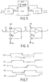
Le registre de base qui peut être utilisé pour stocker un bit de donnée est représenté à la figure 6.The basic register that can be used to store a data bit is shown in Figure 6.
Il comprend deux étages identiques en cascade et il est commandé par quatre signaux d'horloge de période t = T/p; ces signaux sont représentés à la figure 7; ils sont produits à partir d'une horloge CLK de période T/p; les signaux K1 et Q1 commandent le premier étage du registre; les signaux K2 et Q2 commandent le deuxième étage.It comprises two identical stages in cascade and is controlled by four clock signals of period t = T / p; these signals are shown in Figure 7; they are produced from a CLK clock of period T / p; signals K1 and Q1 control the first stage of the register; signals K2 and Q2 control the second stage.
K1 est sensiblement identique au signal CLK; K2 est obtenu simplement par inversion de CLK; Q1 est un signal ayant une transition vers le niveau logique bas après la transition de K1 vers le niveau logique haut et ayant une transition vers le niveau haut retardée par rapport à la transition vers le bas de Q2; Q2 a, vis-à-vis de K2 et Q1, la même relation que Q1 vis-à-vis de K1 et Q2.K1 is substantially identical to the CLK signal; K2 is obtained simply by inverting CLK; Q1 is a signal having a transition to the low logic level after the transition from K1 to the high logic level and having a transition to the high level delayed with respect to the down transition from Q2; Q2 has, with respect to K2 and Q1, the same relation as Q1 with respect to K1 and Q2.
Chaque étage du registre élémentaire de la figure 6 est constitué comme on le voit sur la figure d'un premier transistor a canal N en série entre l'entrée de l'étage et l'entrée d'un inverseur; ce transistor est commandé par le signal Q1 (Q2 pour le deuxième étage); la sortie de l'inverseur est rebouclée d'une part sur la grille d'un transistor à canal P inséré entre une source de tension Vdd et l'entrée de l'inverseur; d'autre part sur la grille d'un transistor à canal N; ce dernier est en série entre une borne de masse Vss et un autre transistor à canal N relié par ailleurs à l'entrée de l'inverseur et commandé par le signal K1 (ou K2 pour le deuxième étage).Each stage of the elementary register of FIG. 6 is constituted as seen in the figure of a first transistor with N channel in series between the input of the stage and the input of an inverter; this transistor is controlled by the signal Q1 (Q2 for the second stage); the output of the inverter is looped back on the one hand to the gate of a P channel transistor inserted between a voltage source Vdd and the input of the inverter; on the other hand on the gate of an N channel transistor; the latter is in series between a ground terminal Vss and another N-channel transistor also connected to the input of the inverter and controlled by the signal K1 (or K2 for the second stage).
La figure 8 montre un circuit avec neuf inverseurs et deux portes NOR permettant de générer les signaux K1, Q1, K2, Q2 à partir d'un signal d'horloge CLK symétrique de période T/p.FIG. 8 shows a circuit with nine inverters and two NOR gates making it possible to generate the signals K1, Q1, K2, Q2 from a clock signal CLK of symmetrical period T / p.
La figure 9 montre comment on réalise un registre REG(i,j) à partir de m x p registres élémentaires lorsque les données comprennent p bits en série sur un bus de m conducteurs en parallèle; chaque rectangle sur la figure 9 représente un registre élémentaire de stockage d'un bit, c'est-à-dire qu'un rectangle correspond au circuit à deux étages de la figure 6.FIG. 9 shows how a REG (i, j) register is produced from m x p elementary registers when the data comprises p bits in series on a bus of m conductors in parallel; each rectangle in FIG. 9 represents an elementary storage register of a bit, that is to say that a rectangle corresponds to the two-stage circuit of FIG. 6.
L'entrée du registre REG(i,j) se fait par un bus de m conducteurs, chaque conducteur arrivant à l'entrée d'un ensemble respectif de p registres élémentaires en cascade; il y a m ensembles en parallèle correspondant chacun à un conducteur du bus d'entrée; la sortie du dernier registre de chaque ensemble en cascade constitue un conducteur de sortie du registre REG(i,j); la sortie globale du registre REG(i,j) est un bus de m conducteurs constitué par les conducteurs de sortie des m ensembles en parallèle.The REG register (i, j) is entered by a bus of m conductors, each conductor arriving at the input of a set respective of p cascade elementary registers; there are am sets in parallel each corresponding to a conductor of the input bus; the output of the last register of each cascade assembly constitutes an output conductor of the REG register (i, j); the global output of the REG register (i, j) is a bus of m conductors constituted by the output conductors of the m assemblies in parallel.
Tous les registres élémentaires du registre REG(i,j) ainsi d'ailleurs que des autres registres de la mémoire sont commandés par les mêmes signaux K1,Q1,K2,Q2.All the elementary registers of the register REG (i, j) as well as elsewhere of the other registers of the memory are controlled by the same signals K1, Q1, K2, Q2.
Les multiplexeurs comportent dans ce cas une première entrée constituée par un bus de m conducteurs, une deuxième entrée constituée par un bus de m conducteurs, et une sortie constituée par un bus de m conducteurs, le bus de sortie étant relié au bus de la première entrée pendant la phase a et au bus de la deuxième entrée pendant la phase b.The multiplexers in this case comprise a first input constituted by a bus of m conductors, a second input constituted by a bus of m conductors, and an output constituted by a bus of m conductors, the output bus being connected to the bus of the first input during phase a and the second input bus during phase b.
Claims (4)
Applications Claiming Priority (2)
| Application Number | Priority Date | Filing Date | Title |
|---|---|---|---|
| FR8709458 | 1987-07-03 | ||
| FR8709458A FR2617621B1 (en) | 1987-07-03 | 1987-07-03 | TRANSPOSITION MEMORY FOR DATA PROCESSING CIRCUIT |
Publications (2)
| Publication Number | Publication Date |
|---|---|
| EP0298002A1 true EP0298002A1 (en) | 1989-01-04 |
| EP0298002B1 EP0298002B1 (en) | 1992-05-27 |
Family
ID=9352847
Family Applications (1)
| Application Number | Title | Priority Date | Filing Date |
|---|---|---|---|
| EP88420230A Expired - Lifetime EP0298002B1 (en) | 1987-07-03 | 1988-06-29 | Transposition memory for a data processing circuit |
Country Status (6)
| Country | Link |
|---|---|
| US (1) | US4903231A (en) |
| EP (1) | EP0298002B1 (en) |
| JP (1) | JP2994390B2 (en) |
| KR (1) | KR890002782A (en) |
| DE (1) | DE3871442D1 (en) |
| FR (1) | FR2617621B1 (en) |
Cited By (2)
| Publication number | Priority date | Publication date | Assignee | Title |
|---|---|---|---|---|
| FR2674666A1 (en) * | 1991-03-29 | 1992-10-02 | Ricoh Kk | TWO DIMENSIONAL SHIFTING NETWORK. |
| EP0439412B1 (en) * | 1990-01-26 | 1997-05-14 | STMicroelectronics S.A. | Serializer/deserializer |
Families Citing this family (15)
| Publication number | Priority date | Publication date | Assignee | Title |
|---|---|---|---|---|
| US5301345A (en) * | 1991-05-03 | 1994-04-05 | Motorola, Inc. | Data processing system for performing a shifting operation and a constant generation operation and method therefor |
| US5483475A (en) * | 1993-09-15 | 1996-01-09 | Industrial Technology Research Institute | Fast pipelined 2-D discrete cosine transform architecture |
| US5350018A (en) * | 1993-10-07 | 1994-09-27 | Dowell Schlumberger Incorporated | Well treating system with pressure readout at surface and method |
| US5481487A (en) * | 1994-01-28 | 1996-01-02 | Industrial Technology Research Institute | Transpose memory for DCT/IDCT circuit |
| KR0175733B1 (en) * | 1995-11-01 | 1999-04-15 | 이준 | Vlsi for transforming beat serial matrix |
| KR100239349B1 (en) | 1996-12-20 | 2000-01-15 | 구자홍 | Data format transformation circuit |
| US5938763A (en) * | 1997-08-06 | 1999-08-17 | Zenith Electronics Corporation | System for transposing data from column order to row order |
| US6175892B1 (en) | 1998-06-19 | 2001-01-16 | Hitachi America. Ltd. | Registers and methods for accessing registers for use in a single instruction multiple data system |
| US6460112B1 (en) | 1999-02-23 | 2002-10-01 | Netlogic Microsystems, Llc | Method and apparatus for determining a longest prefix match in a content addressable memory device |
| EP1107107A1 (en) * | 1999-12-10 | 2001-06-13 | Koninklijke Philips Electronics N.V. | Parallel data processing and shuffling |
| KR100346763B1 (en) * | 2000-02-19 | 2002-08-01 | 구광익 | The system to do work obtaining burning gas energy as resolve water electrolysis |
| KR100355311B1 (en) * | 2000-09-04 | 2002-10-11 | 더블유에스이 주식회사 | Gas producing device by electroysis react |
| US7024414B2 (en) * | 2001-08-06 | 2006-04-04 | Sensage, Inc. | Storage of row-column data |
| US11036827B1 (en) * | 2017-10-17 | 2021-06-15 | Xilinx, Inc. | Software-defined buffer/transposer for general matrix multiplication in a programmable IC |
| CN109408117B (en) * | 2018-10-08 | 2021-01-26 | 京东方科技集团股份有限公司 | Matrix transposing device and method, and display device |
Citations (2)
| Publication number | Priority date | Publication date | Assignee | Title |
|---|---|---|---|---|
| US3535694A (en) * | 1968-01-15 | 1970-10-20 | Ibm | Information transposing system |
| US4302775A (en) * | 1978-12-15 | 1981-11-24 | Compression Labs, Inc. | Digital video compression system and methods utilizing scene adaptive coding with rate buffer feedback |
Family Cites Families (1)
| Publication number | Priority date | Publication date | Assignee | Title |
|---|---|---|---|---|
| US4791598A (en) * | 1987-03-24 | 1988-12-13 | Bell Communications Research, Inc. | Two-dimensional discrete cosine transform processor |
-
1987
- 1987-07-03 FR FR8709458A patent/FR2617621B1/en not_active Expired
-
1988
- 1988-06-27 KR KR1019880007803A patent/KR890002782A/en not_active Application Discontinuation
- 1988-06-28 JP JP63158233A patent/JP2994390B2/en not_active Expired - Fee Related
- 1988-06-29 DE DE8888420230T patent/DE3871442D1/en not_active Expired - Fee Related
- 1988-06-29 EP EP88420230A patent/EP0298002B1/en not_active Expired - Lifetime
- 1988-07-01 US US07/214,252 patent/US4903231A/en not_active Expired - Lifetime
Patent Citations (2)
| Publication number | Priority date | Publication date | Assignee | Title |
|---|---|---|---|---|
| US3535694A (en) * | 1968-01-15 | 1970-10-20 | Ibm | Information transposing system |
| US4302775A (en) * | 1978-12-15 | 1981-11-24 | Compression Labs, Inc. | Digital video compression system and methods utilizing scene adaptive coding with rate buffer feedback |
Cited By (2)
| Publication number | Priority date | Publication date | Assignee | Title |
|---|---|---|---|---|
| EP0439412B1 (en) * | 1990-01-26 | 1997-05-14 | STMicroelectronics S.A. | Serializer/deserializer |
| FR2674666A1 (en) * | 1991-03-29 | 1992-10-02 | Ricoh Kk | TWO DIMENSIONAL SHIFTING NETWORK. |
Also Published As
| Publication number | Publication date |
|---|---|
| JPH01258066A (en) | 1989-10-16 |
| DE3871442D1 (en) | 1992-07-02 |
| KR890002782A (en) | 1989-04-11 |
| JP2994390B2 (en) | 1999-12-27 |
| US4903231A (en) | 1990-02-20 |
| EP0298002B1 (en) | 1992-05-27 |
| FR2617621B1 (en) | 1989-12-01 |
| FR2617621A1 (en) | 1989-01-06 |
Similar Documents
| Publication | Publication Date | Title |
|---|---|---|
| EP0298002B1 (en) | Transposition memory for a data processing circuit | |
| EP3660849B1 (en) | Memory circuit suitable for performing computing operations | |
| EP0712133B1 (en) | Method of anticipated reading of a serial accessed memory and related memory | |
| EP0151653A1 (en) | Series-parallel/parallel-series device for variable bit length configuration | |
| FR2787233A1 (en) | Verifying integrity of decoding circuits of memory matrix by performing at least N or M writing of second words in storage in such way that every line and every column has at least registered second word | |
| FR2479508A1 (en) | GROUP-ELEMENTS DATA PROCESSING DEVICE AND SWITCHING CIRCUITS REDUCING THE NUMBER OF CONNECTIONS BETWEEN ELEMENTS | |
| EP0014151A1 (en) | Method of treating successive signal samples and digital filter for carrying out the method | |
| EP0920157A1 (en) | Device for managing a shared buffer memory | |
| FR2565382A1 (en) | DATA REORGANIZATION APPARATUS | |
| EP1803061A1 (en) | Reconfigurable, modular and hierarchical parallel processor system | |
| EP0183610B1 (en) | Read-write memory and its use in a linear interpolation circuit | |
| EP0674444B1 (en) | Filter for matrix of pixels | |
| EP3503104B1 (en) | Memory circuit suitable for performing computing operations | |
| FR2772160A1 (en) | CIRCUIT FOR CALCULATING FAST FOURIER TRANSFORMATION AND REVERSE QUICK FOURIER TRANSFORMATION | |
| FR2556902A1 (en) | Method and device for specified rank filtering of a digital signal and application to separable two-dimensional median filtering. | |
| EP1542233A1 (en) | Serial memory comprising means for protecting an extended memory range during a write operation | |
| EP0407311A1 (en) | Data merging circuit | |
| FR2540261A1 (en) | Parallel multiplier in MOS integrated circuit of the pipe-line type | |
| EP1249843A2 (en) | Test method for serial access memory and corresponding serial memory | |
| FR2710777A1 (en) | Electronic memory device with sequential access. | |
| EP0046105B1 (en) | Fast digital operator device | |
| EP0376769B1 (en) | Apparatus for line-column matrix transposition using shift registers and permutation operators | |
| EP0500481B1 (en) | Circuit and method for selecting the k largest data of a sequence of data | |
| EP0274323A1 (en) | Integrated signal-processing circuit for line and column summation of matrices of numerical values | |
| FR2602073A1 (en) | DIGITAL SIGNAL PROCESSING CIRCUIT FOR COSINUS TRANSFORMATION. |
Legal Events
| Date | Code | Title | Description |
|---|---|---|---|
| PUAI | Public reference made under article 153(3) epc to a published international application that has entered the european phase |
Free format text: ORIGINAL CODE: 0009012 |
|
| AK | Designated contracting states |
Kind code of ref document: A1 Designated state(s): DE FR GB IT NL |
|
| 17P | Request for examination filed |
Effective date: 19890621 |
|
| 17Q | First examination report despatched |
Effective date: 19910424 |
|
| GRAA | (expected) grant |
Free format text: ORIGINAL CODE: 0009210 |
|
| ITF | It: translation for a ep patent filed |
Owner name: MARCHI & MITTLER S.R.L. |
|
| AK | Designated contracting states |
Kind code of ref document: B1 Designated state(s): DE FR GB IT NL |
|
| PG25 | Lapsed in a contracting state [announced via postgrant information from national office to epo] |
Ref country code: NL Effective date: 19920527 |
|
| GBT | Gb: translation of ep patent filed (gb section 77(6)(a)/1977) | ||
| REF | Corresponds to: |
Ref document number: 3871442 Country of ref document: DE Date of ref document: 19920702 |
|
| NLV1 | Nl: lapsed or annulled due to failure to fulfill the requirements of art. 29p and 29m of the patents act | ||
| PLBE | No opposition filed within time limit |
Free format text: ORIGINAL CODE: 0009261 |
|
| STAA | Information on the status of an ep patent application or granted ep patent |
Free format text: STATUS: NO OPPOSITION FILED WITHIN TIME LIMIT |
|
| 26N | No opposition filed | ||
| REG | Reference to a national code |
Ref country code: FR Ref legal event code: D6 |
|
| REG | Reference to a national code |
Ref country code: GB Ref legal event code: IF02 |
|
| PGFP | Annual fee paid to national office [announced via postgrant information from national office to epo] |
Ref country code: DE Payment date: 20020702 Year of fee payment: 15 |
|
| PGFP | Annual fee paid to national office [announced via postgrant information from national office to epo] |
Ref country code: FR Payment date: 20030610 Year of fee payment: 16 |
|
| PGFP | Annual fee paid to national office [announced via postgrant information from national office to epo] |
Ref country code: GB Payment date: 20030625 Year of fee payment: 16 |
|
| PG25 | Lapsed in a contracting state [announced via postgrant information from national office to epo] |
Ref country code: DE Free format text: LAPSE BECAUSE OF NON-PAYMENT OF DUE FEES Effective date: 20040101 |
|
| PG25 | Lapsed in a contracting state [announced via postgrant information from national office to epo] |
Ref country code: GB Free format text: LAPSE BECAUSE OF NON-PAYMENT OF DUE FEES Effective date: 20040629 |
|
| GBPC | Gb: european patent ceased through non-payment of renewal fee |
Effective date: 20040629 |
|
| PG25 | Lapsed in a contracting state [announced via postgrant information from national office to epo] |
Ref country code: FR Free format text: LAPSE BECAUSE OF NON-PAYMENT OF DUE FEES Effective date: 20050228 |
|
| REG | Reference to a national code |
Ref country code: FR Ref legal event code: ST |
|
| PG25 | Lapsed in a contracting state [announced via postgrant information from national office to epo] |
Ref country code: IT Free format text: LAPSE BECAUSE OF NON-PAYMENT OF DUE FEES;WARNING: LAPSES OF ITALIAN PATENTS WITH EFFECTIVE DATE BEFORE 2007 MAY HAVE OCCURRED AT ANY TIME BEFORE 2007. THE CORRECT EFFECTIVE DATE MAY BE DIFFERENT FROM THE ONE RECORDED. Effective date: 20050629 |