EP0286352B1 - Entry point mapping and skipping method and apparatus - Google Patents
Entry point mapping and skipping method and apparatus Download PDFInfo
- Publication number
- EP0286352B1 EP0286352B1 EP19880303012 EP88303012A EP0286352B1 EP 0286352 B1 EP0286352 B1 EP 0286352B1 EP 19880303012 EP19880303012 EP 19880303012 EP 88303012 A EP88303012 A EP 88303012A EP 0286352 B1 EP0286352 B1 EP 0286352B1
- Authority
- EP
- European Patent Office
- Prior art keywords
- instruction
- address
- incrementing
- macro
- microcode
- Prior art date
- Legal status (The legal status is an assumption and is not a legal conclusion. Google has not performed a legal analysis and makes no representation as to the accuracy of the status listed.)
- Expired - Lifetime
Links
Images
Classifications
-
- G—PHYSICS
- G06—COMPUTING; CALCULATING OR COUNTING
- G06F—ELECTRIC DIGITAL DATA PROCESSING
- G06F9/00—Arrangements for program control, e.g. control units
- G06F9/06—Arrangements for program control, e.g. control units using stored programs, i.e. using an internal store of processing equipment to receive or retain programs
- G06F9/22—Microcontrol or microprogram arrangements
- G06F9/26—Address formation of the next micro-instruction ; Microprogram storage or retrieval arrangements
- G06F9/261—Microinstruction address formation
-
- G—PHYSICS
- G06—COMPUTING; CALCULATING OR COUNTING
- G06F—ELECTRIC DIGITAL DATA PROCESSING
- G06F9/00—Arrangements for program control, e.g. control units
- G06F9/06—Arrangements for program control, e.g. control units using stored programs, i.e. using an internal store of processing equipment to receive or retain programs
- G06F9/22—Microcontrol or microprogram arrangements
- G06F9/26—Address formation of the next micro-instruction ; Microprogram storage or retrieval arrangements
-
- G—PHYSICS
- G06—COMPUTING; CALCULATING OR COUNTING
- G06F—ELECTRIC DIGITAL DATA PROCESSING
- G06F9/00—Arrangements for program control, e.g. control units
- G06F9/06—Arrangements for program control, e.g. control units using stored programs, i.e. using an internal store of processing equipment to receive or retain programs
- G06F9/30—Arrangements for executing machine instructions, e.g. instruction decode
- G06F9/30145—Instruction analysis, e.g. decoding, instruction word fields
Definitions
- Map circuit 12 could be implemented to accommodate a particular instruction set so that the number of micro-instruction addresses allocated to a particular macro-instruction varies. This would require that either the instruction set be fixed at the time the map is fixed or that the map circuit itself be programmable.
- Fig. 3 actually shows three skips in the skipping region, although any other number could be used.
Description
- The present invention relates to methods and apparatus for mapping a macro-instruction to a microcode instruction memory.
- Many computers today execute instructions by storing a number of microcode instructions for each macro-instruction in a microcode memory. The microcode instructions are then executed for the particular macro-instruction to implement the macro-instruction. A typical method is shown in Fig. 1, where a macro-instruction is placed into an operation
code instruction register 10. The instruction inregister 10 is then decoded by amapping circuit 12 to produce an address which is provided to amicrocode memory 14. This address will be the address of the first micro-instruction in a series of micro-instructions to implement the particular macro-instruction. The remaining micro-instructions are obtained by incrementing the firstmicro-instruction address 16 by one after that micro-instruction is executed to produce successive micro-instructions 18, 20 and 22 for the macro-instruction. An example of this typical prior art method is given at pages 61-62 of the article in Microprocessors and Microsystems, Vol.4, N°2, March 1980, pages 57-62. - In one implementation, each macro-instruction is allocated a fixed number of micro-instructions. If this fixed number is four, for instance, then any macro-instruction which requires more than four micro-instructions must include a jump in the last micro-instruction to a separate area of the
microcode memory 14. A jump is undesirable because it places additional requirements on the microcode in terms of time or space. To do a jump, a jump address must be specified, and this requires space. In addition, another clock cycle may be required for a jump. To avoid the requirement of a jump, enough space can be allocated to accommodate the largest macro-instruction, but this results in a large number of wasted memory spaces for macro-instructions which require less than the maximum number of micro-instructions. Alternately, the microcode memory could be divided into groups of different fixed sizes with the sizes varying by a power of two (i.e., groups of four, eight, sixteen, etc.). Thus, a short macro-instruction could be allocated for microcode addresses 16-22 as shown in Fig. 1, while a longer macro-instruction can be allocated eight microcode memory addresses starting atlocation 23 as shown in Fig. 1. Numbers of microcode addresses which are not a power of two cannot be accommodated without requiring additional circuitry formapping circuit 12. A power of two implementation can be done simply by blocking out unwanted bits to result in a higher number. -
Map circuit 12 could be implemented to accommodate a particular instruction set so that the number of micro-instruction addresses allocated to a particular macro-instruction varies. This would require that either the instruction set be fixed at the time the map is fixed or that the map circuit itself be programmable. - The present invention uses a fixed entry-point map to produce an entry point address of a first micro-instruction for a particular macro-instruction. That address is then incremented by a fixed number, such as 512, to produce the second, third, etc. micro-instructions for that macro-instruction. After a fixed number of these 512 address skips, such as 6, the addresses are incremented by 1 so that successive micro-instructions are in adjacent address locations.
- The determination of whether to increment the address by 512 or by 1 is done by a decode circuit which simply looks at the current address to determine whether it is in the skipping region of the microcode memory or the successive incrementing region. The present invention thus provides flexibility to the micro-instruction addressing with the minimal addition of circuitry. In addition, the method of the present invention allows the entry point map to be fixed, and thus there is no need for it to be programmable.
- The macro-instructions are arranged so that any macro-instruction requiring more than six micro-instructions is followed by one or more macro-instructions which require six or less micro-instructions. Thus, when the first macro-instruction starts executing the micro-instructions in the increment by one region of memory, these memory addresses will be available since the next succeeding macro-instructions will not extend that far.
- Alternately, a variable skipping region can be used to give more flexibility. This flexibility enables the skipping regions to be determined when the code is written, thus enabling the optimization of memory space. A variable skipping region implementation requires a slightly more complex method of determining whether the address should be an increment of one or a skip increment upon returns from subroutine calls, since it is not simply dependent upon the fixed address.
- For a fuller understanding of the nature and advantages of the invention, reference should be made to the ensuing detailed description taken in conjunction with the accompanying drawings.
-
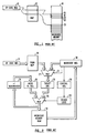
- Fig. 1 is a diagram of a microcode memory mapping scheme of the prior art;
- Fig. 2 is a block diagram of a prior art microcode addressing circuit;
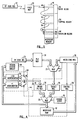
- Fig. 3 is a diagram of a microcode mapping scheme according to the present invention; and
- Fig. 4 is a block diagram of a microcode addressing scheme according to the present invention.
- Fig. 2 shows one type of implementation of microcode address generation according to the prior art which will aid in understanding the present invention. An operation code register 24 stores a macro-instruction which is decoded by a
map circuit 26 to provide a microcode memory address to targetregister 28.Map circuit 26 is shown as being a programmable read-only memory (PROM), but could take other forms.Target register 28 receives the initial address frommap circuit 26 throughmultiplexer 27 and provides it through amultiplexer 30 to themicrocode memory 32. The micro-instruction at that address is provided tomicrocode register 38. The address is then incremented by a +1incrementer 34 which is then provided to a microprogram counter register 36. This incremented address is provided throughmultiplexer 30 back tomemory 32 to provide the next micro-instruction tomicrocode register 38. This type of incrementing continues until there is a jump or other instruction which is detected bydecode logic 40. Typically, a jump is executed by providing a jump address frommicrocode register 38 to multiplexer 27. Aselect signal 37 is provided frommicrocode register 38 to select the microcode jump address frommicrocode register 38 which is then provided to targetregister 28. A control bit or bits are latched intocontrol register 39 which are then decoded bydecode logic 40.Decode logic 40 then provides a select signal to multiplexer 30 to select a jump address intarget register 28 as opposed to the incrementing address from microprogram counter register 36. At the end of a micro-instruction, an instruction dispatch jump is done in which selectsignal 37 frommultiplexer 27 selects the next instruction address frommap circuit 26, and a new instruction is then executed. - Fig. 3 is a diagram of a microcode memory mapping scheme according to the present invention. An
operation code register 42 is provided to hold a macro-instruction. Afixed map 44 decodes the macro-instruction to produce an address to amicrocode memory 46. The first address provided is anentry point address 48 in anentry block 50. The next micro-instruction is found by incrementingaddress 48 by a fixed number to produce asecond address 52. This address is in turn incremented by the same number to produce athird address 54. These addresses are located in a skippingregion 56, which, in one embodiment, includes six skips for each macro-instruction (only three are shown in Fig. 3). After the six skips, anaddress 58 is incremented by one to produceaddresses 60 and 62 in succession in an overflow region 64. - This mapping scheme provides flexibility for mapping macro-instructions having different numbers of micro-instructions. For instance, if
entry point address 48 is address 212 and the macro-instructions having entry point addresses of 213 and 214 are less than six micro-instructions long, then addresslocations 60 and 62 will be blank, allowing the macro-instructions starting ataddress 48 to have eight micro-instructions. By appropriate placement of the starting address of each macro-instruction, the instructions can be mapped to make optimum use of the memory by appropriate programming of the microcode while at the same time allowing for a simplefixed map 44 because of the fixed entry point address for each macro-instruction. The use of a fixed entry point allows smaller, faster logic to be used. The logic is high speed because less logic is required than a RAM or PROM. In addition, because the logic is special purpose, it takes up less space than a RAM or PROM, which is especially important when the circuit is put on an integrated circuit. - A block diagram of a circuit to implement the mapping scheme of Fig. 3 is shown in Fig. 4. The block diagram of Fig. 4 follows the basic structure of that of Fig. 2. However, instead of using a +1
incrementer 34 as in Fig. 2, avariable incrementer 66 is used with a memory region decodecircuit 68.Variable incrementer 66 includes a +1 incrementer 70 and a +512incrementer 72 as well as a multiplexer 74. In operation, the address provided tomicrocode RAM 32 is incremented by 512 byincrementer 72 with the new address being passed through multiplexer 74 to microcodeprogram counter register 36. This process continues until memory region decodecircuit 68 detects that the address corresponds to overflow region 64 of Fig. 3. At this point, decodecircuit 68 provides a select signal to multiplexer 74 to select the output of +1incrementer 70. Accordingly, thereafter the address tomicrocode RAM 32 is incremented by 1 as shown in Fig. 3. - Although
variable incrementer 66 is shown as a pair of incrementers and a multiplexer for sake of understanding, it can be implemented with a single counter which allows for multiple carry bit inputs.Region decode circuit 68 can simply select a position of the carry bit to vary the increment.Decode circuit 68 only needs to look at the upper bits of the address to determine whether it is in overflow region 64. - Although a 512 increment which is repeated six times is shown, any other numbers could be used. Fig. 3 actually shows three skips in the skipping region, although any other number could be used.
- In an alternate embodiment, the skipping region of Fig. 3 can be made of variable length. This provides additional flexibility when the microcode is programmed. For instance, if a number of instructions requiring only a few address locations each, such as three each, are grouped together, then a block of memory in the section which would normally correspond to the fourth address location for each instruction is freed for other uses.
- In one implementation of a variable skipping region, skipping is done until there is a jump or branch in the program. In this case, upon a return from the jump or branch, the skipping incrementer is no longer used and the +1 incrementer is used. As shown in Fig. 4, an extra bit can be stored in a
position 41 shown in phantom attached tomicro PC register 36. A control line frombit position 41 is provided to multiplexer 74. This control line replaces the select line from region decodecircuit 68, which would not be used in this implementation. Upon a branch, a bit is stored inposition 41 and upon return from branch, this bit selectsincrementer 70 by the appropriate control signal to multiplexer 74. Typically, the branch address is stored in a return stack (not shown). The extra bit is positioned in the return address stack so that when the address is provided tomicro PC register 36, this bit is inposition 41. The input tobit position 41 is provided bycontrol signal line 37, shown in phantom. The loading of this bit intomicro PC register 36 is done by a load control signal from control register 39 (shown in phantom). - The variable skipping embodiment thus allows variation in the number of address locations per instruction while still maintaining the fixed entry point mapping system. This flexibility allows changes to be made to the microcode as it becomes more complicated or simpler by adjusting the skipping region. In addition, regions which are not a power of two with respect to each other can be used, since the determination of the region length is done by the positioning of the jump instruction, and not by the addition of circuitry to the mapping circuit.
- As will be understood by those familiar with the art, the present invention may be embodied in other specific forms without departing from the spirit or essential characteristics thereof. For example, instead of using a decoding circuit to determine whether the address is in the skipping region or the overflow region, a counter could be used to count the number of skipping increments by
incrementer 72. The variable skipping region could also be implemented in different ways, such as by using a bit in the microcode instruction so that the skipping region is not dependent upon jumps. Accordingly, the disclosure of the preferred embodiments of the invention is intended to be illustrative, but not limiting, of the scope of the invention which is set forth in the following claims.
Claims (19)
- A method for implementing a macro-instruction by addressing a series of microcode instructions in a memory comprising the steps of:a) providing an entry point address of said memory in response to said macro-instruction;b) incrementing said entry point address by a first predetermined number to provide an address of a next microcode instruction in said memory;c) repeating step b) for a second number of times to produce successive microcode instructions;d) incrementing said microcode instruction address by one after incrementing said address said second number of times;e) repeating step d) for a remaining number of microcode instructions for said macro-instruction.
- The method of claim 1 wherein said second number is fixed.
- The method of claim 2 further comprising the steps of incrementing said microcode instruction address by one during jumps, said incrementing during jumps being excluded from said second number.
- The method of claim 2 wherein said first predetermined number is 512.
- The method of claim 2 wherein said second predetermined number is five.
- The method of claim 2 further comprising the step of arranging said entry point address for a plurality of macro-instructions such that a macro-instruction having a third number of microcode instructions more than said second number plus one is followed by said third number of macro-instructions having a number of microcode instructions less than or equal to said second number plus one.
- The method of claim 1 wherein said second number is variable.
- The method of claim 7 wherein said second number is a number of microcode instructions up to a first jump.
- An apparatus for implementing a macro-instruction by addressing a series of microcode instructions in a memory comprising:
an instruction register for holding said macro-instruction;
means, responsive to said macro-instruction, for providing an entry point address of said memory;
first means for incrementing said address by a first predetermined number;
second means for incrementing said address by one; and
means for coupling an output of said first means for incrementing to said memory for a second number of increments of said address and thereafter coupling said second means for incrementing to said memory. - The apparatus of claim 9 wherein said second number is fixed.
- The apparatus of claim 10 wherein said means for providing an entry point address is permanently fixed.
- The apparatus of claim 10 wherein said first number is 512.
- The apparatus of claim 10 wherein said second number is six.
- The apparatus of claim 10 wherein said first and second means for incrementing comprise a single counter having multiple carry inputs.
- The apparatus of claim 10 wherein said means for coupling comprises a decode circuit responsive to a portion of a current microcode memory address to produce a signal to select said first means for incrementing for a first block of addresses and said second means for incrementing for a second block of addresses.
- The apparatus of claim 9 wherein said second number is variable.
- The apparatus of claim 16 wherein said means for coupling comprises a bit output of a micro program counter register, said bit output corresponding to a bit input, and further comprising a microcode instruction register having an output coupled to said bit input.
- The apparatus of claim 17 wherein said bit output has a separate load enable, and further comprising a control register having an input coupled to said microcode instruction register and an output coupled to said load enable.
- An apparatus for implementing a macro-instruction by addressing a series of microcode instructions in a memory comprising:
an instruction register for holding said macro-instruction;
means, responsive to said macro-instruction, for providing a fixed entry point address of said memory;
first means for incrementing said address by a first predetermined number;
second means for incrementing said address by one; and
a decode circuit responsive to a portion of a current microcode memory address to produce a signal to select said first means for incrementing for a first block of addresses and said second means for incrementing for a second block of addresses.
Applications Claiming Priority (2)
| Application Number | Priority Date | Filing Date | Title |
|---|---|---|---|
| US3660687A | 1987-04-10 | 1987-04-10 | |
| US36606 | 1987-04-10 |
Publications (3)
| Publication Number | Publication Date |
|---|---|
| EP0286352A2 EP0286352A2 (en) | 1988-10-12 |
| EP0286352A3 EP0286352A3 (en) | 1990-08-29 |
| EP0286352B1 true EP0286352B1 (en) | 1995-01-11 |
Family
ID=21889561
Family Applications (1)
| Application Number | Title | Priority Date | Filing Date |
|---|---|---|---|
| EP19880303012 Expired - Lifetime EP0286352B1 (en) | 1987-04-10 | 1988-04-05 | Entry point mapping and skipping method and apparatus |
Country Status (4)
| Country | Link |
|---|---|
| EP (1) | EP0286352B1 (en) |
| JP (1) | JP2804266B2 (en) |
| AU (1) | AU607481B2 (en) |
| DE (1) | DE3852708T2 (en) |
Families Citing this family (2)
| Publication number | Priority date | Publication date | Assignee | Title |
|---|---|---|---|---|
| EP0574980B1 (en) * | 1992-06-15 | 1999-06-09 | Koninklijke Philips Electronics N.V. | Time-discrete signal processor |
| US8214754B2 (en) * | 2005-04-15 | 2012-07-03 | Microsoft Corporation | Registration of applications and complimentary features for interactive user interfaces |
Family Cites Families (1)
| Publication number | Priority date | Publication date | Assignee | Title |
|---|---|---|---|---|
| JPS59183433A (en) * | 1982-12-06 | 1984-10-18 | Sanyo Electric Co Ltd | Central processor of microprogram control system |
-
1988
- 1988-04-05 DE DE19883852708 patent/DE3852708T2/en not_active Expired - Fee Related
- 1988-04-05 EP EP19880303012 patent/EP0286352B1/en not_active Expired - Lifetime
- 1988-04-08 AU AU14437/88A patent/AU607481B2/en not_active Ceased
- 1988-04-11 JP JP63088895A patent/JP2804266B2/en not_active Expired - Lifetime
Also Published As
| Publication number | Publication date |
|---|---|
| JP2804266B2 (en) | 1998-09-24 |
| DE3852708D1 (en) | 1995-02-23 |
| AU1443788A (en) | 1988-10-13 |
| DE3852708T2 (en) | 1995-06-01 |
| EP0286352A3 (en) | 1990-08-29 |
| JPS644833A (en) | 1989-01-10 |
| AU607481B2 (en) | 1991-03-07 |
| EP0286352A2 (en) | 1988-10-12 |
Similar Documents
| Publication | Publication Date | Title |
|---|---|---|
| US5896529A (en) | Branch prediction based on correlation between sets of bunches of branch instructions | |
| US5931940A (en) | Testing and string instructions for data stored on memory byte boundaries in a word oriented machine | |
| EP0114304B1 (en) | Vector processing hardware assist and method | |
| US5032983A (en) | Entry point mapping and skipping method and apparatus | |
| US4388682A (en) | Microprogrammable instruction translator | |
| EP0297897A2 (en) | A microinstruction sequencer capable of instructing arithmetic, logical and data move operations in a conditional manner | |
| US4446517A (en) | Microprogram memory with page addressing and address decode in memory | |
| US4370729A (en) | Microprogram sequencer | |
| US4251862A (en) | Control store organization in a microprogrammed data processing system | |
| US3979725A (en) | Multi-way program branching circuits | |
| EP0035334B1 (en) | Data processing system with two level microprogramming | |
| EP0086992A2 (en) | Microword generation mechanism utilizing separate programmable logic arrays | |
| US4424563A (en) | Data processor including a multiple word processing method and device | |
| EP0229734A2 (en) | Microprogram control device | |
| US4128872A (en) | High speed data shifter array | |
| JPH02242334A (en) | Computer apparatus to be microprogrammed and addressing of microcode sequence memory | |
| EP0286352B1 (en) | Entry point mapping and skipping method and apparatus | |
| US5124910A (en) | Microprogram control apparatus for generating a branch condition signal to be designated by a micro-branch instruction | |
| EP0164418B1 (en) | Microprogram control system | |
| US4750108A (en) | Data processor unit comprising a control section which comprises an address generator for generating addresses which are composed of characteristic address portions | |
| JPH04283834A (en) | Address generator for data memory of processor | |
| US6920544B2 (en) | Processor and instruction execution method with reduced address information | |
| US4675843A (en) | Programmable logic controller | |
| EP0843253B1 (en) | A method for reducing the number of bits needed for the representation of constant values in a data processing device | |
| US4931989A (en) | Microword generation mechanism utilizing a separate programmable logic array for first microwords |
Legal Events
| Date | Code | Title | Description |
|---|---|---|---|
| PUAI | Public reference made under article 153(3) epc to a published international application that has entered the european phase |
Free format text: ORIGINAL CODE: 0009012 |
|
| AK | Designated contracting states |
Kind code of ref document: A2 Designated state(s): DE FR GB IT SE |
|
| PUAL | Search report despatched |
Free format text: ORIGINAL CODE: 0009013 |
|
| AK | Designated contracting states |
Kind code of ref document: A3 Designated state(s): DE FR GB IT SE |
|
| 17P | Request for examination filed |
Effective date: 19901218 |
|
| 17Q | First examination report despatched |
Effective date: 19940429 |
|
| GRAA | (expected) grant |
Free format text: ORIGINAL CODE: 0009210 |
|
| AK | Designated contracting states |
Kind code of ref document: B1 Designated state(s): DE FR GB IT SE |
|
| REF | Corresponds to: |
Ref document number: 3852708 Country of ref document: DE Date of ref document: 19950223 |
|
| ET | Fr: translation filed | ||
| ITF | It: translation for a ep patent filed |
Owner name: PROPRIA PROTEZIONE PROPR. IND. |
|
| PLBE | No opposition filed within time limit |
Free format text: ORIGINAL CODE: 0009261 |
|
| STAA | Information on the status of an ep patent application or granted ep patent |
Free format text: STATUS: NO OPPOSITION FILED WITHIN TIME LIMIT |
|
| 26N | No opposition filed | ||
| PGFP | Annual fee paid to national office [announced via postgrant information from national office to epo] |
Ref country code: SE Payment date: 19990322 Year of fee payment: 12 |
|
| PGFP | Annual fee paid to national office [announced via postgrant information from national office to epo] |
Ref country code: DE Payment date: 20000403 Year of fee payment: 13 |
|
| PGFP | Annual fee paid to national office [announced via postgrant information from national office to epo] |
Ref country code: GB Payment date: 20000405 Year of fee payment: 13 |
|
| PG25 | Lapsed in a contracting state [announced via postgrant information from national office to epo] |
Ref country code: SE Free format text: LAPSE BECAUSE OF NON-PAYMENT OF DUE FEES Effective date: 20000406 |
|
| EUG | Se: european patent has lapsed |
Ref document number: 88303012.4 |
|
| PG25 | Lapsed in a contracting state [announced via postgrant information from national office to epo] |
Ref country code: GB Free format text: LAPSE BECAUSE OF NON-PAYMENT OF DUE FEES Effective date: 20010405 |
|
| GBPC | Gb: european patent ceased through non-payment of renewal fee |
Effective date: 20010405 |
|
| PG25 | Lapsed in a contracting state [announced via postgrant information from national office to epo] |
Ref country code: DE Free format text: LAPSE BECAUSE OF NON-PAYMENT OF DUE FEES Effective date: 20020201 |
|
| PGFP | Annual fee paid to national office [announced via postgrant information from national office to epo] |
Ref country code: FR Payment date: 20040408 Year of fee payment: 17 |
|
| PG25 | Lapsed in a contracting state [announced via postgrant information from national office to epo] |
Ref country code: IT Free format text: LAPSE BECAUSE OF NON-PAYMENT OF DUE FEES;WARNING: LAPSES OF ITALIAN PATENTS WITH EFFECTIVE DATE BEFORE 2007 MAY HAVE OCCURRED AT ANY TIME BEFORE 2007. THE CORRECT EFFECTIVE DATE MAY BE DIFFERENT FROM THE ONE RECORDED. Effective date: 20050405 |
|
| PG25 | Lapsed in a contracting state [announced via postgrant information from national office to epo] |
Ref country code: FR Free format text: LAPSE BECAUSE OF NON-PAYMENT OF DUE FEES Effective date: 20051230 |
|
| REG | Reference to a national code |
Ref country code: FR Ref legal event code: ST Effective date: 20051230 |