EP0276113A2 - Code device recognition system and access control system using such recognition system - Google Patents
Code device recognition system and access control system using such recognition system Download PDFInfo
- Publication number
- EP0276113A2 EP0276113A2 EP88300382A EP88300382A EP0276113A2 EP 0276113 A2 EP0276113 A2 EP 0276113A2 EP 88300382 A EP88300382 A EP 88300382A EP 88300382 A EP88300382 A EP 88300382A EP 0276113 A2 EP0276113 A2 EP 0276113A2
- Authority
- EP
- European Patent Office
- Prior art keywords
- coil
- code
- code device
- control circuit
- circuit
- Prior art date
- Legal status (The legal status is an assumption and is not a legal conclusion. Google has not performed a legal analysis and makes no representation as to the accuracy of the status listed.)
- Withdrawn
Links
Images


Classifications
-
- H—ELECTRICITY
- H03—ELECTRONIC CIRCUITRY
- H03K—PULSE TECHNIQUE
- H03K17/00—Electronic switching or gating, i.e. not by contact-making and –breaking
- H03K17/94—Electronic switching or gating, i.e. not by contact-making and –breaking characterised by the way in which the control signals are generated
- H03K17/945—Proximity switches
- H03K17/95—Proximity switches using a magnetic detector
- H03K17/952—Proximity switches using a magnetic detector using inductive coils
- H03K17/9537—Proximity switches using a magnetic detector using inductive coils in a resonant circuit
- H03K17/954—Proximity switches using a magnetic detector using inductive coils in a resonant circuit controlled by an oscillatory signal
-
- G—PHYSICS
- G07—CHECKING-DEVICES
- G07C—TIME OR ATTENDANCE REGISTERS; REGISTERING OR INDICATING THE WORKING OF MACHINES; GENERATING RANDOM NUMBERS; VOTING OR LOTTERY APPARATUS; ARRANGEMENTS, SYSTEMS OR APPARATUS FOR CHECKING NOT PROVIDED FOR ELSEWHERE
- G07C9/00—Individual registration on entry or exit
- G07C9/00174—Electronically operated locks; Circuits therefor; Nonmechanical keys therefor, e.g. passive or active electrical keys or other data carriers without mechanical keys
- G07C9/00309—Electronically operated locks; Circuits therefor; Nonmechanical keys therefor, e.g. passive or active electrical keys or other data carriers without mechanical keys operated with bidirectional data transmission between data carrier and locks
-
- H—ELECTRICITY
- H03—ELECTRONIC CIRCUITRY
- H03K—PULSE TECHNIQUE
- H03K17/00—Electronic switching or gating, i.e. not by contact-making and –breaking
- H03K17/94—Electronic switching or gating, i.e. not by contact-making and –breaking characterised by the way in which the control signals are generated
- H03K17/945—Proximity switches
- H03K17/95—Proximity switches using a magnetic detector
- H03K17/951—Measures for supplying operating voltage to the detector circuit
-
- H—ELECTRICITY
- H03—ELECTRONIC CIRCUITRY
- H03K—PULSE TECHNIQUE
- H03K17/00—Electronic switching or gating, i.e. not by contact-making and –breaking
- H03K17/94—Electronic switching or gating, i.e. not by contact-making and –breaking characterised by the way in which the control signals are generated
- H03K17/945—Proximity switches
- H03K17/95—Proximity switches using a magnetic detector
- H03K17/952—Proximity switches using a magnetic detector using inductive coils
- H03K17/9525—Proximity switches using a magnetic detector using inductive coils controlled by an oscillatory signal
-
- G—PHYSICS
- G07—CHECKING-DEVICES
- G07C—TIME OR ATTENDANCE REGISTERS; REGISTERING OR INDICATING THE WORKING OF MACHINES; GENERATING RANDOM NUMBERS; VOTING OR LOTTERY APPARATUS; ARRANGEMENTS, SYSTEMS OR APPARATUS FOR CHECKING NOT PROVIDED FOR ELSEWHERE
- G07C9/00—Individual registration on entry or exit
- G07C9/00174—Electronically operated locks; Circuits therefor; Nonmechanical keys therefor, e.g. passive or active electrical keys or other data carriers without mechanical keys
- G07C2009/00753—Electronically operated locks; Circuits therefor; Nonmechanical keys therefor, e.g. passive or active electrical keys or other data carriers without mechanical keys operated by active electrical keys
- G07C2009/00769—Electronically operated locks; Circuits therefor; Nonmechanical keys therefor, e.g. passive or active electrical keys or other data carriers without mechanical keys operated by active electrical keys with data transmission performed by wireless means
- G07C2009/00777—Electronically operated locks; Circuits therefor; Nonmechanical keys therefor, e.g. passive or active electrical keys or other data carriers without mechanical keys operated by active electrical keys with data transmission performed by wireless means by induction
Landscapes
- Engineering & Computer Science (AREA)
- Computer Networks & Wireless Communication (AREA)
- Physics & Mathematics (AREA)
- General Physics & Mathematics (AREA)
- Near-Field Transmission Systems (AREA)
Abstract
A code device recognition system comprises a transmitting coil (12) driven by an oscillator (14), an overlapping receiving coil (13) connected to a detector, and a code device (11) including a coil (15). The overlap of the coils is arranged so that the receiving coil is not magnetically coupled with the transmitting coil. The code device includes a switch element (16) for completing a circuit through the coil (15) and a control device for operating this switch element in a predetermined code sequence. When the code device is within range of the transmitting and receiving coils, it creates a secondary magnetic field, detectable by a detector connected to the receiving coil, only when the switch element is closed. The detector can thus read the code and compare it with at least one stored code to issue a recognition signal. The coil (15) also preferably drives a rectifier circuit to provide power for the control circuit 17.
Description
- This invention relates to a code device recognition system which is suitable for operating door locks and other systems for controlling access to buildings or parts of buildings.
- Various code device reading systems are currently in use which make use of punched or magnetically or otherwise coded cards and the like to control locks and the like. Such systems normally require the user to insert the key card into a slot in a reading device or otherwise present for reading.
- Locking systems also exist in which the key contains a power source which is used to energise a transmitting device, such as an infra-red radiation emitter which can transmit a coded signal to a code recognition device incorporated in a lock. Such keys consume significant quantities of electrical energy and require periodic recharging or replacement of the power source.
- In accordance with the invention there is provided a code device recognition system comprising a transmitter device for creating an alternating magnetic field in a zone adjacent said transmitter device; at least one code device including a coil, a switching element interconnecting the ends of said coil and a control circuit for said switching element, said control circuit operating to switch the switching element on and off in accordance with a predetermined code; and a detector device arranged to detect when the switching element of the code device is switched on within the alternating magnetic field and to compare the coded signal detected with at least one acceptable code.
- Preferably the coil of the code device is also connected to a rectifier circuit arranged to supply power to said control circuit.
- Preferably the transmitter device and the detector device each includes a flat coil, the transmitter coil and the receiver coil being arranged in an overlapping relationship such that the receiver coil is in a null position relative to the transmitter coil.
- An example of the invention is shown in the accompanying drawings in which:
- Figure 1 is a simplified block diagram showing a code device recognition system included in an access control system;
- Figure 2 is a detailed circuit diagram of an oscillator included in the system;
- Figure 3 is a detailed circuit diagram of a detector included in the system;
- Figure 4 is a flow chart for software used by a microcomputer included in the detector of Figure 3; and
- Figure 5 is a detailed circuit diagram of a code device included in the system of Figure 1.
- Referring firstly to Figure 1, the access control system includes a number of
lock stations 10 each controlling the lock of a door and a plurality ofcode devices 11 for issue to the persons who require to open the doors. Generally, eachcode device 11 is preset to have a different code associated with it and each lock station is provided with a memory device of some type which stores data representing the codes of all the coded devices which are to be permitted to cause opening of the associated lock. - The
lock station 10 includes two flat, overlapping multi-turn coils, one, 12, of which is a transmitting coil, and the other, 13, of which is a receiving coil. These two coils are arranged relative to one another so that thereceiving coil 13 is at a null position relative to thecoil 12, which is driven by anoscillator 14 so as to produce an alternating magnetic field in a zone adjacent the lock station. Such null position is found by adjusting the overlap of the two coils until there is no alternating voltage induced in thereceiving coil 13 as a result of the alternating magnetic field created by thecoil 12. - The
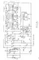
oscillator 14 is shown in detail in Figure 2. The oscillator includes an npn transistor TR₁ which has its base connected to the junction of two resistors R₁ and R₂ which are connected in series between a +12V rail and ground. The collector of transistor TR₁ is connected to a point on the winding 12 which, in the example shown, has 38 turns. The connection between the collector of transistor TR₁ and thecoil 12 is eighteen turns from one end of the coil. Another point on the coil, one turn further from said one end, is connected to the +12V rail. The other end ofcoil 12 is connected by a resistor R₃ and a capacitor C₁ in series to the base of the transistor TR₁ and a further capacitor C₂ connects the base of transistor TR₁ to the ground rail. A capacitor C₃ is connected between said other point on thecoil 12 and the ground rail. A capacitor C₄ is connected across theentire coil 12. A resistor R₄ connects the emitter of transistor TR₁ to the ground rail. - The oscillator is a Hartley-type oscillator. The resistor R₁ provides a low level initial current at power-up to start the oscillator running. Resistors R₂ and R₃ and capacitors C₁ and C₂ form a Wien bridge circuit which applies to the base of transistor TR₁ a positive feedback signal. Connection of the collector of transistor TR₁ to a point just one turn from the power supply connection instead of to the more usual point at the "lower" end of the
coil 12, enables the circuit to operate as a power oscillator. The resistor R₄ limits the current in transistor TR₁. - The system of Figure 1 also includes the
code device 11 which is shown in detail in Figure 5. In principle, the code device includes acoil 15, aswitch device 16 connected to complete a circuit through the coil and acontrol circuit 17 for theswitch device 16. When thecode device 11 is within the aforementioned zone adjacent the transmittingcoil 12 an alternating e.m.f. is induced in thecoil 15. When theswitch device 16 is closed alternating current can flow in thecoil 15 which creates its own alternating magnetic field which induces an e.m.f. in thereceiving coil 13. When theswitch device 16 is open however, no such current can flow and no e.m.f. is induced in thereceiving coil 13. Thecontrol circuit 17 is arranged so as, when thecoil 15 is within the zone, it opens and closes the switch element in a sequence dependent on a code stored in the control circuit. - The code device is ideally in form of a credit-card size plastics card with the
coil 15 wound around its periphery and theswitch device 16 andcontrol circuit 17 included as a single chip integrated circuit (possibly with some discrete components) mounted on the card and connected to the coil. The following description, however, relates to a prototype control circuit in which conventional integrated circuit components are used. The skilled reader will understand that the various components identified can readily be incorporated in a special purpose integrated circuit. The control circuit described not only controls theswitch device 16, but also includes a rectifier and voltage multiplier circuit to enable the e.m.f. induced in thecoil 15 when theswitch device 16 is open, to provide power for the control circuit. No battery is thus required. - The detailed circuit of the control circuit, shown in Figure 5, includes a CMOS analog gate device (part of a 4066 type CMOS integrated circuit) as the
switch device 16. Thecoil 15 has a capacitor C₁₁ connected across it, such that thecoil 15 and capacitor C₁₁ form a series resonant circuit which is tuned to the frequency of the oscillator 14 (which may, for example, be in the region of 135KHz). The rectifier and voltage multiplier circuit referred to above comprises two diodes D₁ and D₄ which connect one end ofcoil 15 to opposite ends of a series circuit comprising two capacitors C₁₂ and C₁₃. The common point of these two capacitors is connected to the other end ofcoil 15. The capacitors C₁₂ and C₁₃ act as storage devices and are charged by thecoil 15 to positive and negative peak voltages respectively so that the total voltage across the two capacitors in series is almost equal to the peak-to-peak voltage induced in thecoil 15. The series circuit consisting of the two capacitors C₁₂ and C₁₃ is connected between two power supply rails, 20, 21. - A zener diode D₅ has its cathode connected to
rail 20 and its anode connected by a resistor R₆ to therail 21. The anode of zener diode D₅ is connected to the gate terminal of a mosfet T₂ which actually forms part of a 4007 type CMOS integrated circuit. The drain terminal of this mosfet is connected to therail 21 and its source terminal is connected to the gate terminal of another mosfet T₃ forming part of the same integrated circuit. The drain terminal of the mosfet T₃ is connected to therail 20 and its source terminal is connected to arail 20 a . The drain terminal of the mosfet T₂ is also connected to the gate terminal of a third mosfet T₁ forming yet another part of the same integrated circuit. The drain terminal of mosfet T₁ is connected torail 20 and its source terminal is connected to therail 20 a . In addition a resistor R₇ connects therail 20 to the gates of mosfets T₁ and T₃ and a resistor R₈ connects the source terminal of mosfet T₁ to the gate of the mosfet T₂. - Initially, when the code device is not in the alternating magnetic field, the three mosfets are all biased off by resistors R₆ and R₇. When the voltage between
rails - The
rail 20 a provides the power supply to another CMOS integrated circuit (type 4093) which consists of two Schmitt input NAND gates G₁ and G₂. The gate G₁ has its two inputs connected together and connected by a resistor R₉ to therail 20 a and by a capacitor C₁₄ to therail 21. When the mosfet T₃ turns on as described above, power is supplied to the gate G₁, but since the capacitor C₁₄ is initially in a discharged state the output of gate G₁ is initially high. After a delay determined by the time constant of R₉ and C₁₄, the output of the gate G₂ goes low. The gate G₁ output is used for initialising the succeeding parts of the control circuits. - These parts consist of a clock oscillator in the form of a CMOS multivibrator integrated circuit 22 (type 4047) and a shift register consisting of three cascaded CMOS parallel-in, serial out static shift register integrated
circuits - The output of gate G₁ is connected to the parallel/serial control terminal of all three shift register integrated circuits and to the external reset and trigger input of the multivibrator integrated
circuit 22. During the time for which the output of gate G₁ is high the clock oscillator is disabled, but the shift registers 23 to 25 are loaded with parallel data from a codeselect array 26. This array comprises a series of connections from the various parallel data input terminals of the shift registers 23 to 25 either to therail 20 a or to therail 21 in accordance with whether the associated bit of the code is to be a 1 or a 0. The first bit is always a 1. When the output of gate G₁ goes low, the oscillator starts to run and the code is clocked bit by bit from the serial output terminal ofshift register circuit 25. - This serial output terminal is connected to the control terminal of the
analog gate 16. This gate has its signal terminals connected in series with a pair of oppositely connected diodes D₂ and D₃ across thecoil 15. Thus when the code bit is a 1 thegate 16 is conductive and when it is a 0 thegate 16 is non-conductive and the code is thus transmitted. A resistor R₁₀ connects the control terminal of thegate 16 to rail 21 to keepgate 16 non-conductive except when signals are received from the shift register. - The other gate G₂ is used to reset the control circuit after an interval longer than that required to transmit the code. Gate G₂ has its inputs connected together and connected by a capacitor C₁₅ to the
rail 20 a and by a resistor R₁₁ to therail 21. When mosfet T₃ turns on the output of gate G₂ is held low for a time dependent on the time constant of resistor R₁₁ and capacitor C₁₅. The output of gate G₂ is connected to the control terminal of another analog gate 27 (forming part of the aforementioned 4066-type CMOS i.c.) which has its signal path connected across the capacitor C₁₄. - When the output of gate G₂ goes high after transmission has been completed the
analog gate 27 discharges not only capacitor C₁₄, but also the power supply storage capacitors C₁₂ and C₁₃ so that the whole cycle recommences. - It is of significance, as will be explained hereinafter, that the time taken between a reset and the next initialisation pulse from gate G₁ is dependent on the magnetic field strength and therefore on the distance between the code device and the transmitting coil. This variable time delay results from the rate of charging of the capacitors C₁₂ and C₁₃ being dependent on the e.m.f. induced in the
coil 15. - The receiving
coil 13 of Figure 1 is connected to a detector which is shown in detail in Figure 3. The detector includes a capacitor C₂₁ connected across thecoil 13 and forming a series tuned circuit tuned to the frequency of theoscillator 14. A diode D₁₁ has its anode connected to one end of thecoil 13 and its cathode connected by a capacitor C₂₂ to the other end of coil 13 (which other end is grounded). A resistor R₂₁ is connected across the capacitor C₂₂ and a d.c. blocking capacitor C₂₃ connects the cathode of the diode D₁₁ to the non-inverting input terminal of an operational amplifier A₁. A resistor R₂₂ connects this non-inverting input terminal to ground. The inverting input of amplifier A₁ is connected to ground by a resistor R₂₃ and to the amplifier output terminal by a resistor R₂₄. The resistors R₂₃ and R₂₄ are chosen to provide a gain of about 100. - The output of amplifier A₁ is connected to a low pass filter constituted by resistors R₂₅ and R₂₆, capacitors C₂₄, C₂₅ and C₂₆ and an operational amplifier A₂. This filter has a cut-off frequency of about 200Hz and serves to prevent the detector from acting as a simple metal detector (detecting changes of position of a metal object passing through the zone).
- The output of amplifier A₂ is connected to the non-inverting input of a voltage comparator A₃, the inverting input of which is connected to a reference voltage source comprising two resistors R₂₇ and R₂₈ in series between a +12V supply rail and ground. The comparator A₃ has its output connected to an input terminal of a single chip microcomputer 30 (such as a 6805 integrated circuit).
- The diode D₁₁ and capacitor C₂₂ form a peak store which is discharged by the resistor R₂₁. The a.c. component of the signal on resistor R₂₁ is amplified and filter and formed into a well squared waveform by the comparator A₃.
- The microcomputer is required to receive the trains of pulses from the comparator A₃ (which pulse trains represent the codes stored in code device which pass through the zone) and determine whether any such code is an acceptable code for the door in question.
- Figure 4 shows a simplified flow chart of software installed in a ROM area in the microcomputer. The software distinguishes signals from the comparator from signals received at an RS232 input of the computer, reads the code bit by bit into its memory, compares this with stored codes and outputs a lock release signal if a match is found.
- As shown the software checks 100 whether the output of A₃ is low periodically. (Since the filter amplifier A₂ is connected to operate in inverting mode a low signal from comparator A₃ corresponds to a bit value of 1 in the code sequence emitted by the code device). If it is not a
check 101 is made to establish if an input byte has been received at the RS232 port. If such a byte has been received the RS232 command is processed before returning to theoriginal check 100. - If the A₃ output is found to be low then a
code input routine 102 is started by setting a counter I to 16 and looping through a bit by bit input sequence with an appropriate delay in the loop. When the counter I has counted out acheck 103 is made to compare the variable CARDNO, established by rotating the individual A₃ output states in successive executions of the loop into the LSB of CARDNO, with numbers stored in the ROM of the microcomputer. If no match is found the program returns to step 100 otherwise a lock release signal isoutput 104 before such return. - It will be understood by the skilled reader that the code device recognition system described above is capable of very considerable elaboration. For example the software may include the steps of measuring the duration of the first bit of the code (which is always 1) and using this measurement to establish the delay required in the
loop 102. - It will also be understood that the very simple embodiment described is not suitable for the transmission of the whole range of 2¹⁶ codes capable of being recognised by the microcomputer. For example a code consisting of all 1s or all 0s cannot be used. Various known techniques, such as the use of Manchester codes, can be used to extend the range of codes available.
- The very simple code receiving algorithm used means that the microcomputer will simply sample the A₃ output at sixteen equally spaced instants. If there happen to be two code devices within range of the transmitter at the same time, the code collected could therefore be a mixture of the codes from the two code devices. The variable delay between transmission cycles from the code devices overcomes this problem. Since the transmissions from the two code devices will restart following different delay periods a complete transmission from each key will eventually be properly collected and used to operate the lock if it matches a stored code.
- Code sequences longer than 16 bits can, of course, be used if required.
- The computer program may, of course, be extended to include many other functions if required, such as the recordal of dates and times of usage of the various code devices.
- It is worthy of note that, when the system of the invention is used in an access control system, there is no need for the holder of the card to take any action to initiate unlocking of a door. He may simply carry the code device in a pocket and, provided the card is not magnetically shielded by anything he is carrying the lock will automatically open on his approach (if it is intended that he should have access to the area controlled by that lock).
Claims (9)
1. A code device recognition system comprising a transmitter device for creating an alternating magnetic field in a zone adjacent said transmitter device; at least one code device including a coil, a switching element interconnecting the ends of said coil and a control circuit for said switching element, said control circuit operating to switch the switching element on and off in accordance with a predetermined code; and a detector device arranged to detect when the switching element of the code device is switched on within the alternating magnetic field and to compare the coded signal detected with at least one acceptable code.
2. A system as claimed in claim 1 in which the coil of said code device is also connected to a rectifier circuit arranged to supply power to said control circuit.
3. A system as claimed in claim 2 in which said control circuit includes initialising means sensitive to said rectifier circuit for initiating a code transmission sequence.
4. A system as claimed in claim 3 in which said control circuit also includes reset means for resetting said initialising means after a predetermined time lapse.
5. A system as claimed in claim 1 in which there is a delay between resetting and re-initialising dependent on the strength of the magnetic field in which the code device is located.
6. A system as claimed in claim 1 in which said transmitter device and said detector device each includes a flat coil, the transmitter coil and the receiver coil being arranged in an overlapping relationship such that the receiver coil is in a null position relative to the transmitter coil.
7. A system as claimed in claim 6 in which said detector device includes a low pass filter arranged to prevent detection of ordinary metal objects in said zone.
8. A system as claimed in claim 1 in which the code device is in the form of a plastics card with the coil around its periphery and the control circuit and switch element mounted on the card.
9. A system as claimed in claim 1 in which the code device includes a capacitor connected to said coil and forming in combination therewith a series resonant circuit tuned to the frequency of said oscillator.
Applications Claiming Priority (2)
| Application Number | Priority Date | Filing Date | Title |
|---|---|---|---|
| GB878701221A GB8701221D0 (en) | 1987-01-21 | 1987-01-21 | Card operated lock |
| GB8701221 | 1987-01-21 |
Publications (2)
| Publication Number | Publication Date |
|---|---|
| EP0276113A2 true EP0276113A2 (en) | 1988-07-27 |
| EP0276113A3 EP0276113A3 (en) | 1990-08-08 |
Family
ID=10610956
Family Applications (1)
| Application Number | Title | Priority Date | Filing Date |
|---|---|---|---|
| EP88300382A Withdrawn EP0276113A3 (en) | 1987-01-21 | 1988-01-19 | Code device recognition system and access control system using such recognition system |
Country Status (2)
| Country | Link |
|---|---|
| EP (1) | EP0276113A3 (en) |
| GB (1) | GB8701221D0 (en) |
Cited By (9)
| Publication number | Priority date | Publication date | Assignee | Title |
|---|---|---|---|---|
| GR900100775A (en) * | 1990-10-26 | 1992-09-25 | I D A Control Pikis Pan & Sia | Independent electronic system for electric energy saving in private and let places |
| EP0774673A3 (en) * | 1995-11-16 | 2000-07-12 | Kabushiki Kaisha Tokai-Rika-Denki-Seisakusho | Transmission-reception system |
| GB2358427A (en) * | 2000-01-21 | 2001-07-25 | Roke Manor Research | Automatic locking |
| WO2002009284A1 (en) * | 2000-07-20 | 2002-01-31 | Honeywell Control Systems Limited | Inductive proximity sensor and related methods |
| DE10318350B3 (en) * | 2003-04-23 | 2004-12-09 | Werner Turck Gmbh & Co. Kg | Inductive proximity switch, has transmission coil with circular coil surface having periphery overlapped by annular coil surface of reception coil |
| DE102006046437A1 (en) * | 2006-09-25 | 2008-04-10 | Euchner Gmbh + Co. Kg | Monitoring device for safety mechanism e.g. safety switches for protective door has coupling element through which read head and actuator cooperate in electrically contactless manner |
| EP2031566A1 (en) | 2007-09-03 | 2009-03-04 | Burg-Wächter Kg | Method for operating a system with at least one electronic lock |
| EP2071523A1 (en) | 2007-12-03 | 2009-06-17 | Faciliteam AG | Method for releasing a radio lock |
| WO2024043290A1 (en) * | 2022-08-25 | 2024-02-29 | Next Innovation合同会社 | Switch mechanism and power-on method |
Citations (3)
| Publication number | Priority date | Publication date | Assignee | Title |
|---|---|---|---|---|
| GB1160672A (en) * | 1966-03-23 | 1969-08-06 | Donovan Electrical Company Ltd | Improvements relating to Proximity Detectors |
| GB2079842A (en) * | 1980-07-10 | 1982-01-27 | Nat Res Dev | Locks |
| GB2158870A (en) * | 1984-05-17 | 1985-11-20 | Waertsilae Oy Ab | Locking system |
-
1987
- 1987-01-21 GB GB878701221A patent/GB8701221D0/en active Pending
-
1988
- 1988-01-19 EP EP88300382A patent/EP0276113A3/en not_active Withdrawn
Patent Citations (3)
| Publication number | Priority date | Publication date | Assignee | Title |
|---|---|---|---|---|
| GB1160672A (en) * | 1966-03-23 | 1969-08-06 | Donovan Electrical Company Ltd | Improvements relating to Proximity Detectors |
| GB2079842A (en) * | 1980-07-10 | 1982-01-27 | Nat Res Dev | Locks |
| GB2158870A (en) * | 1984-05-17 | 1985-11-20 | Waertsilae Oy Ab | Locking system |
Cited By (15)
| Publication number | Priority date | Publication date | Assignee | Title |
|---|---|---|---|---|
| GR900100775A (en) * | 1990-10-26 | 1992-09-25 | I D A Control Pikis Pan & Sia | Independent electronic system for electric energy saving in private and let places |
| EP0774673A3 (en) * | 1995-11-16 | 2000-07-12 | Kabushiki Kaisha Tokai-Rika-Denki-Seisakusho | Transmission-reception system |
| GB2358427A (en) * | 2000-01-21 | 2001-07-25 | Roke Manor Research | Automatic locking |
| GB2358427B (en) * | 2000-01-21 | 2004-01-21 | Roke Manor Research | Automatic locking system |
| US7719262B2 (en) | 2000-07-20 | 2010-05-18 | Honeywell International Inc. | Inductive proximity sensor and related methods |
| WO2002009284A1 (en) * | 2000-07-20 | 2002-01-31 | Honeywell Control Systems Limited | Inductive proximity sensor and related methods |
| US7969141B2 (en) | 2000-07-20 | 2011-06-28 | Honeywell International Inc. | Inductive proximity sensor and related methods |
| DE10318350B3 (en) * | 2003-04-23 | 2004-12-09 | Werner Turck Gmbh & Co. Kg | Inductive proximity switch, has transmission coil with circular coil surface having periphery overlapped by annular coil surface of reception coil |
| DE10318350C5 (en) * | 2003-04-23 | 2010-08-19 | Werner Turck Gmbh & Co. Kg | Inductive proximity switch |
| DE102006046437A1 (en) * | 2006-09-25 | 2008-04-10 | Euchner Gmbh + Co. Kg | Monitoring device for safety mechanism e.g. safety switches for protective door has coupling element through which read head and actuator cooperate in electrically contactless manner |
| DE102006046437B4 (en) * | 2006-09-25 | 2009-04-09 | Euchner Gmbh + Co. Kg | Device for monitoring the state of a safety-related device |
| EP2031566A1 (en) | 2007-09-03 | 2009-03-04 | Burg-Wächter Kg | Method for operating a system with at least one electronic lock |
| EP2071523A1 (en) | 2007-12-03 | 2009-06-17 | Faciliteam AG | Method for releasing a radio lock |
| DE102007058367B4 (en) * | 2007-12-03 | 2017-10-19 | Faciliteam Ag | Method for releasing a radio lock |
| WO2024043290A1 (en) * | 2022-08-25 | 2024-02-29 | Next Innovation合同会社 | Switch mechanism and power-on method |
Also Published As
| Publication number | Publication date |
|---|---|
| EP0276113A3 (en) | 1990-08-08 |
| GB8701221D0 (en) | 1987-02-25 |
Similar Documents
| Publication | Publication Date | Title |
|---|---|---|
| US4752776A (en) | Identification system | |
| EP0297688B1 (en) | Electronic identification system | |
| US4197524A (en) | Tap-actuated lock and method of actuating the lock | |
| AU642362B2 (en) | Method and apparatus for secure identification and verification | |
| US5245332A (en) | Programmable memory for an encoding system | |
| AU600351B2 (en) | System for the contactless exchange of data | |
| US4591854A (en) | Touch control identification system with portable encoder | |
| US5058161A (en) | Method and apparatus for secure identification and verification | |
| EP0148248B1 (en) | Dual signal electromagnetic article theft detector | |
| EP0276113A2 (en) | Code device recognition system and access control system using such recognition system | |
| CA2034213C (en) | Inductive coupled object identification system and method | |
| US4559529A (en) | Antitheft system with digitally coded signal | |
| WO2002071342A1 (en) | Signal discriminator for wake-up of a low power transponder | |
| US3970824A (en) | Electronic recognition and identification system for identifying a family of codes | |
| GB2129176A (en) | Identification system | |
| WO1996008794A1 (en) | Security code identification circuit | |
| GB2278631A (en) | Identification system | |
| US5856809A (en) | Static antenna tuning and antenna voltage measurement | |
| US4242576A (en) | Electronic identification device | |
| US4713660A (en) | Electronic proximity key and lock | |
| US3958105A (en) | Electronic recognition and identification system for identifying several master keys | |
| KR20010050990A (en) | Passive signal discriminator for wake up of low power transponder | |
| KR100232219B1 (en) | Low voltage sensing circuit | |
| WO1990006024A1 (en) | A communication system | |
| CA1316268C (en) | Programmable memory for an encoding system |
Legal Events
| Date | Code | Title | Description |
|---|---|---|---|
| PUAI | Public reference made under article 153(3) epc to a published international application that has entered the european phase |
Free format text: ORIGINAL CODE: 0009012 |
|
| AK | Designated contracting states |
Kind code of ref document: A2 Designated state(s): AT BE CH DE ES FR GB GR IT LI LU NL SE |
|
| PUAL | Search report despatched |
Free format text: ORIGINAL CODE: 0009013 |
|
| AK | Designated contracting states |
Kind code of ref document: A3 Designated state(s): AT BE CH DE ES FR GB GR IT LI LU NL SE |
|
| STAA | Information on the status of an ep patent application or granted ep patent |
Free format text: STATUS: THE APPLICATION IS DEEMED TO BE WITHDRAWN |
|
| 18D | Application deemed to be withdrawn |
Effective date: 19900801 |