EP0266004A2 - Architecture for power of two coefficient fir filter - Google Patents
Architecture for power of two coefficient fir filter Download PDFInfo
- Publication number
- EP0266004A2 EP0266004A2 EP87202045A EP87202045A EP0266004A2 EP 0266004 A2 EP0266004 A2 EP 0266004A2 EP 87202045 A EP87202045 A EP 87202045A EP 87202045 A EP87202045 A EP 87202045A EP 0266004 A2 EP0266004 A2 EP 0266004A2
- Authority
- EP
- European Patent Office
- Prior art keywords
- coefficient
- filter
- bus
- tap
- output
- Prior art date
- Legal status (The legal status is an assumption and is not a legal conclusion. Google has not performed a legal analysis and makes no representation as to the accuracy of the status listed.)
- Granted
Links
Images


Classifications
-
- H—ELECTRICITY
- H03—ELECTRONIC CIRCUITRY
- H03H—IMPEDANCE NETWORKS, e.g. RESONANT CIRCUITS; RESONATORS
- H03H17/00—Networks using digital techniques
- H03H17/02—Frequency selective networks
- H03H17/06—Non-recursive filters
-
- G—PHYSICS
- G06—COMPUTING; CALCULATING OR COUNTING
- G06F—ELECTRIC DIGITAL DATA PROCESSING
- G06F17/00—Digital computing or data processing equipment or methods, specially adapted for specific functions
- G06F17/10—Complex mathematical operations
- G06F17/15—Correlation function computation including computation of convolution operations
-
- H—ELECTRICITY
- H03—ELECTRONIC CIRCUITRY
- H03H—IMPEDANCE NETWORKS, e.g. RESONANT CIRCUITS; RESONATORS
- H03H17/00—Networks using digital techniques
- H03H17/02—Frequency selective networks
- H03H17/0223—Computation saving measures; Accelerating measures
- H03H17/0227—Measures concerning the coefficients
Definitions
- This invention pertains to the field of nonrecursive digital filters used for digital signal processing and real time digital video processing.
- VLSI very large scale integrated circuits
- FIR finite impulse response
- FIR finite impulse response
- Finite impulse response (FIR) digital filters are widely used in digital signal processing, as well as in real-time digital video processing.
- the conventional hardware realization of an FIR digital filter utilizes the basic functional components of delay units, multipliers and adders.
- multipliers are generally the most complex for hardware realization, and occupy large "real estate" area, which factors increase the cost of the filter.
- the cost of multipliers in discrete component systems is high. From the point of view of VLSI chip design, the area occupied by a multiplier on an IC filter chip is too large. Cost is not the only important factor; the operational speed of a filter is even more significant in a variety of applications; for example, in real-time video processing and other high speed digital signal processing.
- U.S. Patent No. 3,979,701 discloses a non-recursive digital filter composed of a cascaded plurality of basic sections, each of which is characterized by coefficient values of integer powers of two's.
- the filter of this patent uses no multipliers and claims an operating speed several times faster than other filters which utilize multipliers.
- the multiplierless FIR filter disclosed in this application has certain concepts which appear to be similar to those of U.S. Patent No. 3,979,701 but there are important differences.
- the filter described in U.S. Patent No. 3,979,701 has two basic building blocks from which the filter is constructed: Type 1 and Type 2.
- Type 1 unit has only coefficients with a value of 1 (see line 53 to line 56 of column 3 of U.S. Patent No. 3,979,701);
- Type 2 unit has only an even number of delay elements and only three coefficients, the center coefficient value of which is always equal to 1 (see line 7 to line 12 of column 4 of U.S. Patent No. 3,979,701).
- the invention pertains to the architecture and VLSI implementation of an FIR digital filter which contains no multipliers and in which the coefficient space is limited to only powers of two.
- the filter coefficients are linearly quantized to two to the Nth power different levels.
- the filter coefficients are non-linearly quantized to N different levels, each one of which represents a number equal to two to the Nth power.
- Multipliers may be replaced by shift registers and/or multiplexers in this non- conventional design.
- the FIR filter architecture of the present invention uses a structure that is regular and modular. It utilizes for each tap a structure in which three buses go into each tap, the data bus, the coefficient bus and the sum-in bus.
- the data bus brings the broadcast data sample to each tap.
- the coefficient bus contains the weighting factor information.
- the sum-in bus brings the delayed output of the previous tap. Going out of each tap is the sum-out bus, which is the output of each tap and which goes to the sum-in input of the next tap.
- This regular, modular architecture lends itself to cascading of filter sections for larger filters.
- Each tap has a coefficient register which contains the coefficient and control word information for that tap. This information is loaded in the initialization phase of the filter operation.
- Each tap has a shifter which usesthe coefficient for the correct power of two weighting. The output of the shifter is the weighted data sample which is latched in a pipelining latch. the output of the latch is added to the output of the previous tap by an adder. The adder's output is delayed by one time unit and then passed on as the adder input of the next tap.
- the filter words in two phases the initialization phase and the normal operation phase.
- the coefficients and control words are loaded for each tap.
- the coefficient registers are shift registers connected in a serial chain and the loading thereof is serial.
- a non-destructive verification of the loading is accomplished by reading out serially the coefficients and control words and reloading them back in a closed loop simultaneously so that at the end of the verification procedure all coefficients and control words reside in the correct registers.
- This filter uses only powers of two as coefficients. As binary multiplication by powers of two is nothing but a shift of the multiplicand, complex multiplication is replaced by a simple shifter in this case. With the use of only negative powers of two as coefficients, the shift operation is simplified to only right shaft. Assuming the data (multiplicand) is always positive this shifter can handle both positive and negative coefficients.
- the output of this multiplier is one's complement 16 bit data with the most significant bit as sign bit and fifteen magnitude bits, hence keeping the provision of maximum seven bit shift for the eight bit multiplicand, which is equivalent to a multiplication by 2 ⁇ 7. This is the most negative power of two which this multiplier can handle. Otherwise, propertly pogrammed it can multiply the multiplicand with any one of the following values 0, ⁇ 20, ⁇ 2 ⁇ 1, ⁇ 2 ⁇ 2, ... ⁇ 2 ⁇ 7.
- the power-of-two coefficient space can easily be extended beyond the current limit of ⁇ 2 ⁇ 7 by modifying the shifter and certain other elements which handle its output.
- the overall architecture of the shifter does not change; it is only extended to include the increase of coefficient space.
- the architecture is not limited to data words of 8 bits. To increase this to any arbitrary size all that is needed is an increase the size of the NAND gate sets in the shifter from 8 to whatever the desired data size is. Obviously, the ADDER size will have to be increased or decreased according to the maximum value of both the coefficient space and data word size.
- the proposed FIR filter structure is fully programmable for a coefficient space C such that : [C ⁇ ⁇ 0, ⁇ 20, ⁇ 2 ⁇ 1, ⁇ 2 ⁇ 2, ..., ⁇ 2 ⁇ 7 ⁇ ].
- C coefficient space
- all possible shifts of the data inputs are provided for, using a multiplexer whose input is the output of sets of NAND gates, having positive inputs and a selection line.
- Outputs of the NAND gates are shifted and hard-wired to the multiplexer.
- the one's complement conversion of the multiplexer output is accomplished by a set of EXOR gates.
- the filter multiplies a coefficient by a data word without a standard multiplier.
- the filter has been successfully simulated using various coefficients and random data.
- FIR filters are one ofthe most important functions of real time linear signal processing.
- FIR finite impulse response
- transversal filter also called transversal filter.
- the reason for this is that powerful and mature optimization theories exist to aid in the filter design.
- FIR filters can easily be designed to approximate a prescribed magnitude/ frequency response to arbitrary accuracy with an exactly linear phase characteristic.
- the non-recursive FIR filters contain only zeroes in the finite z-plane and hence are always stable. These features make them very attractive for most digital signal processing applications.
- the FIR filter is characterized by the input/output relation.
- T S is the sampling period
- f S 1/T S is the sample rate. So each output sample is the weighted sum of a finite number of input samples (N in Equation 1).
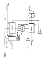
- Figure 1 shows the well known semi- systolic parallel in, serial out transversal filter architecture 20.
- the data is broadcast via a data bus 22 globally to the every tap in the filter, where it is multiplied in multiplier 24 by a weighting factor(the coefficient) from a coefficient register (not shown) appearing on input 23 and added in adder 26 to a delayed output from delay 28 of the previous tap.
- the basic building blocks of any transversal filter 20 are the multiplier 24, the adder 26 and the delay 28. It is this weighting factor multiplier that is eliminated in the architecture of the invention.
- Equation 1 the weighting of the input samples is accomplished by multipliers.
- the multiplier is the most time consuming and expensive building block of the filter, thus there has been a great effort to make multiplication operation cheaper and faster, to increase the overall speed of operation of the filter.
- FIG 2 we will describe the architecture of filter 10 of this invention hierarchically. For example described and illustrated, we use a ten tap filter, a data word of eight bits, a coefficient space from 0 to ⁇ 2 ⁇ 7 and a final output bus 20 bits wide.
- Figure 2 the top level of the hierarchy, shows a ten tap structure of filter 10. Three busses go into each tap 30, the data bus 12, the coefficient bus 14, 15 and the sum-in bus 16. Going out of each tap is the sum-out bus 18. The purpose and function of each bus will be explained in the discussion of the filter operation, but it is clear that the structure is extremely regular and modular. This is an extremely important feature in the architecture from the VLSI implementation point of view.
- the data bus 12 is the bus which brings the broadcast data sample D-IN to each tap 30.
- the coefficient bus is a loop originating at C-I/O gates 41 and includes the C-IN bus 14 and C-OUT bus 15.
- Bus 14 brings the weighting factor information and the sum-in bus 16 brings the delayed output of the previous tap 30.
- the sum-out bus 18 is the output of the tap 30 and can be fed into the sum-in input 16 bus of the next tap 30. Note that this architecture lends itself to cascading very naturally and easily, and is by no means limited to ten taps only.
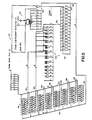
- FIG. 3 shows the building blocks of each tap 30. They will each be explained in detail later, for now we will just identify them.
- the C-REG 32 is the register containing the coefficient and control word information CCW. This information is loaded via the coefficient bus 14 in the initialization phase of the filter operation. Most of this information is used by the SHIFTER 34 for the correct power of two weighting of data from data bus 12.
- the output of the SHIFTER 34 is the weighted data sample, which is latched in a pipelining latch 36, used for speed enhancement purposes.
- the output of the latch 36 is added to the output of the previous tap by the ADDER 38, and the ADDER's output is finally delayed in DELAY 40 by one time unit ofCLK-N before passed on via SUMOUT bus 18 and SUM-IN bus 16 as the ADDER input of the next tap.
- Filter 10 works in two phases: the initialization phase and the normal operation phase.
- the coefficients and control words (CCW) are loaded during the first phase.
- the coefficient and control registers (C-REG) 32 are connected to each other in a serial chain, hence the loading is serial.
- CCW#9 is applied to the coefficient input bus (C-IN) 14 of Figure 2 and Figure 3 and all the C-REG's 32 are clocked by the clock CLK-C 31 (discussed later). It is obvious that CCW#9 will be loaded in C-REG#0.
- CCW#8 is applied to the C-IN bus 14 and all the C-REGs are clocked again.
- CCW#9 shifts from C-REG#0 to C-REG#1 and CCW#8 loaded in C-REG#0. This procedure is repeated ten times. Each time a new CCW is applied to the C-IN bus 14 and all the C-REG's 32 are clocked. That particular CCW, the most recent, is loaded in C-REG#0 and all the other CCW's are shifted to the next C-REG 32 in the serial chain. At the end of the cycle (ten clock pulses in this case), all the CCW are loaded in the correct order in the C-REGs 32.
- the next step is verification of the above loading.
- the purpose is to make sure all the CCW's have been loaded in their required destination registers.
- We utilize a non-destructive verification procedure by which the CCW's are read out for verification and reloaded in a closed loop to the C-REG's 32 simultaneously, so at the end of the verification cycle the CCW's reside back at their respective C-REG's.
- Our verification procedure is also a serial procedure.
- the C-I/O bus is a bidirectional bus, C-IN 14 and C-OUT 15, the direction of which is controlled by an external signal labeled C-RW42.
- coefficient bus 14 acts as an input bus, and for C-RW set to 0, as an output bus 15. It is obvious that for the CCW loading procedure, C-RW is set to 1 and the CCW's are loaded as discussed above.
- the C-RW signal is set to 0 and the CLK-C 31 is clocked.
- the last coefficient (coefficient # 9) appears on C-OUT at the output gates 44 ( Figure 3) and at the same time is loaded back from gates 41 in C-REG # 0.
- the next clock cycle brings the next to last coefficient on the C-OUT bus 15 and simultaneously loads it into C-REG#0 while pushing the current resident of C-REG # 0 (coefficient # 9) to C-REG # 1.
- all the coefficients have been read out from the C-OUT bus 15 through gates 44 and at the same time reloaded in the C-REGs 32 via C-IN bus 14.
- Filter 10 uses only powers of two as coefficients.
- binary multiplication by power of two is a shift of the multiplicand
- complex multiplication is replaced by a simple shifter 34 in this case.
- the shift operation is simplified to only right shift.
- the data (multiplicand) has eight bits and is always positive, and with the assumptions stated supra, this multiplier can handle both positive and negative coefficients.
- Output of this shifter 34 is one's complement 16 bit data with the most significant bit (MSB) as sign bit and fifteen magnitude bits, hence keeping the provision of maximum seven bit shift for the eight bit multiplicand, (an assumption of the example), which is equivalent to a multiplication by 2 ⁇ 7.
- MSB most significant bit
- this multiplier can handle and which the filter requires as well. Otherwise, properly programmed, it can multiply the multiplicand with any one of the following values 0, ⁇ 20, ⁇ 2 ⁇ 1, ⁇ 2 ⁇ 2, ...., ⁇ 2 ⁇ 7.
- Figure 4a shows the format of a control word (CCW) and Figure 4b shows how the shift operation takes place for all positive values of coefficients. These are discussed infra.
- CCW control word
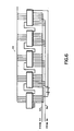
- Figure 5 shows the logic diagram which implements the operation of the above-mentioned one's complement multiplier/shifter 34.
- multiplier/shifter 34 To maintain programmability, we have incorporated in every stage of this multiplier/shifter 34 all possible above-shown shifts and that is done by a simple multiplexing design for multiplier/shifter 34, whose input section 46 consists of eight sets of eight NAND gates. Each of the sets are fed on input lines 47 by the eight magnitude bits of the positive (thus not requiring any sign bit) multiplicand from data bus 12, as shown in the left side of Figure 5.
- Each set of NAND gates has a separate selection line 48 from decoder 62, discussed infra.
- One set of the eight sets of NAND gates 46 will be selected, depending upon the value of the coefficient programmed for that stage in a C-REG 32. Outputs 49 of the selected set of NAND gates 46 are properly shifted and hardwired to the output stage 50 of the shifter/multiplexer 34 to produce a fifteen bit magnitude bus 52 as shown in Figure 5. To avoid clutter in the drawing the output lines of only the first two sets of NAND gates 46 are shown connected.
- the final stage of this circuit 34 is the one's complement conversion logic 54, which is a set of EXOR gates which produces the bit by bit complement of bus 52, in case of negative coefficients, on output bus 56. As the multiplicand is always positive, the sign of the multiplied output on bus 56 depends on that of the coefficient. This sixteen (fifteen bit magnitude together with sign bit) bit bus 56 is latched in latch 36 ( Figure 3) and delivered to the adder 38 ( Figures 3, 6).
- the section following the multiplier/shifter 34 and latch 36 is an adder 38 ( Figure 6) of conventional design. It is a partially (4 bit) full carry look ahead adder cascaded to form a twenty bit adder. It receives the sixteen bit output of multiplier/shifter 34 via pipelining latch 36 as one of its inputs 58, and the other input 60 is the twenty bit output from delay latch 40 of the previous stage.
- the sign-extension technique is used for the smaller number in the adder.
- the sign of the smaller number which is in its one's complement form is also fed to the carry input of the adder, thereby converting the smaller number to its two's complement form.
- the following explanation determines the selection of the size (20 bits) of the larger number.
- this number is the accumulated result of multiplier/shifter outputs of all the stages up to that stage.
- the size (20 bits) is such that it will produce no overflow in the accumulated result of all sixteen stages after cascadation, even if each multiplier/shifter produces the largest possible output 7F80 (that takes place for largest possible eight bit multiplicand FF and the largest possible coefficient 1).
- To achieve this we need one sign bit, fifteen magnitude bits for each multiplied output and log224 bits for the sixteen (24) stage accumulation of them, which is 20 bits in total.
- the FIR filter structure 10 is fully programmable for a coefficient space C such that : [C ⁇ ⁇ 0, ⁇ 20, ⁇ 2 ⁇ 1, ⁇ 2 ⁇ 2, ..., ⁇ 2 ⁇ 7 ⁇ ], under the assumptions of the example described and illustrated.
- the coefficient and control word CCW contains the information of the actual shift, as well as the sign of the coefficient. It also contains information for a coefficient of magnitude 0 (zero).
- the CCW is afive bit word, the three least significant bits, (LSB) defining the power of the coefficient, the next bit controlling the sign and the most significant bit (MSB) for a zero coefficient. This is shown in Figure 4a.
- the three coefficient power control bits pass through a three-to-eight decoder 62 ( Figure 5) and select one shift from 20 to 2 ⁇ 7.
- the sign control bit determines the sign of the coefficient. In case of a zero coefficient (which is a special case since it is not a power of 2) the bit number is set to 1.
- the power-of-two coefficient space can easily be extended beyond the current example limit of ⁇ 2 ⁇ 7 by modifying the shifter 34.
- to increase the space to ⁇ 2 ⁇ 15 requires one more bit for the coefficient value (from 3 to 4) and a 4-to-16 decoder. It also requires sixteen sets of eight NAND gates (instead of the currently used eight sets).
- the overall architecture of the shifter 34 does not change; it is only extended to include the increase of coefficient space.
- filter 10 is not limited to a data word of eight bits. To increase this to any arbitrary size requires only an increase in the number of NAND gates per set from eight to whatever the data size desired is. Obviously, the size of ADDER 38 (number of bits) will have to be increased or decreased according to the maximum value of both the coefficient space and data word size.
- This filter 10 was implemented using Signetics Corporation's 2 micron double metal standard cell technology.
- the current chip has ten taps.
- the IC lay out was performed using Silver Lisco's CAL-MP software. We will now present the simulation results of the various modes of operation of the chip.
- the coefficient clock CLK-C enable signal (CEN) is set to 1. Since, once initialization of the filter has been successfully accomplished, we do not want the coefficients to change, this signal is an added protection against a stray coefficient clock pulse (CLK-C) altering the coefficients. Data is presented via the D-IN bus 12 and the normal operation clock (CLK-N) now becomes the only system clock and filtering is performed on the data.
Landscapes
- Engineering & Computer Science (AREA)
- Physics & Mathematics (AREA)
- Mathematical Physics (AREA)
- Theoretical Computer Science (AREA)
- General Physics & Mathematics (AREA)
- Mathematical Analysis (AREA)
- Computational Mathematics (AREA)
- Computing Systems (AREA)
- Computer Hardware Design (AREA)
- Mathematical Optimization (AREA)
- Pure & Applied Mathematics (AREA)
- Data Mining & Analysis (AREA)
- Algebra (AREA)
- Databases & Information Systems (AREA)
- Software Systems (AREA)
- General Engineering & Computer Science (AREA)
- Complex Calculations (AREA)
- Cable Transmission Systems, Equalization Of Radio And Reduction Of Echo (AREA)
Abstract
Description
- This invention pertains to the field of nonrecursive digital filters used for digital signal processing and real time digital video processing. In particular it pertains to an architectural realization, in the form of very large scale integrated (VLSI) circuits, of finite impulse response (FIR) filters which do not require multipliers and which have only coefficients of two to the Nth power.
- Among the different types of digital filters there has been a great deal of interest in finite impulse response (FIR) digital filters (also called transversal filters). The reason for this is that powerful and mature optimization theories exist to aid in the filter design. FIR filters can easily be designed to approximate a prescribed magnitude/frequency response to arbitrary accuracy with an exactly linear phase characteristic. The nonrecursive FIR filters contain only zeroes in the finite z-plane and hence are always stable. These features make them very attractive for most digital signal processing applications.
- Finite impulse response (FIR) digital filters are widely used in digital signal processing, as well as in real-time digital video processing. The conventional hardware realization of an FIR digital filter utilizes the basic functional components of delay units, multipliers and adders. Among these basic functional components, multipliers are generally the most complex for hardware realization, and occupy large "real estate" area, which factors increase the cost of the filter. The cost of multipliers in discrete component systems is high. From the point of view of VLSI chip design, the area occupied by a multiplier on an IC filter chip is too large. Cost is not the only important factor; the operational speed of a filter is even more significant in a variety of applications; for example, in real-time video processing and other high speed digital signal processing. In the conventional FIR digital filter, a high percentage of the propagation delay time is due to multipliers, which reduce the speed of the filter. Therefore, to improve the operattional speed, reduce the cost and simplify the structural complexity for VLSI chip design, it is desirable to eliminate time-consuming multipliers from digital FIR filters.
- Current technical literature includes numerous articles directed toward the reduction or elimination of multipliers in the architecture or design of FIR digital filters, while at the same time proposing solutions directed to increasing the speed of these filters for use in real time digital signal processing applications.
- In the prior patent art, U.S. Patent No. 3,979,701 discloses a non-recursive digital filter composed of a cascaded plurality of basic sections, each of which is characterized by coefficient values of integer powers of two's. The filter of this patent uses no multipliers and claims an operating speed several times faster than other filters which utilize multipliers.
- The multiplierless FIR filter disclosed in this application has certain concepts which appear to be similar to those of U.S. Patent No. 3,979,701 but there are important differences.
- The filter described in U.S. Patent No. 3,979,701 has two basic building blocks from which the filter is constructed:
Type 1 andType 2. TheType 1 unit has only coefficients with a value of 1 (see line 53 toline 56 ofcolumn 3 of U.S. Patent No. 3,979,701); theType 2 unit has only an even number of delay elements and only three coefficients, the center coefficient value of which is always equal to 1 (seeline 7 toline 12 ofcolumn 4 of U.S. Patent No. 3,979,701). - The invention pertains to the architecture and VLSI implementation of an FIR digital filter which contains no multipliers and in which the coefficient space is limited to only powers of two. In conventional digital filter design, the filter coefficients are linearly quantized to two to the Nth power different levels. In multiplier-free digital filter design, the filter coefficients are non-linearly quantized to N different levels, each one of which represents a number equal to two to the Nth power. Multipliers may be replaced by shift registers and/or multiplexers in this non- conventional design.
- The FIR filter architecture of the present invention uses a structure that is regular and modular. It utilizes for each tap a structure in which three buses go into each tap, the data bus, the coefficient bus and the sum-in bus. The data bus brings the broadcast data sample to each tap. The coefficient bus contains the weighting factor information. The sum-in bus brings the delayed output of the previous tap. Going out of each tap is the sum-out bus, which is the output of each tap and which goes to the sum-in input of the next tap. This regular, modular architecture lends itself to cascading of filter sections for larger filters.
- Each tap has a coefficient register which contains the coefficient and control word information for that tap. This information is loaded in the initialization phase of the filter operation. Each tap has a shifter which usesthe coefficient for the correct power of two weighting. The output of the shifter is the weighted data sample which is latched in a pipelining latch. the output of the latch is added to the output of the previous tap by an adder. The adder's output is delayed by one time unit and then passed on as the adder input of the next tap.
- The filter words in two phases the initialization phase and the normal operation phase. In the initialization phase, the coefficients and control words are loaded for each tap. The coefficient registers are shift registers connected in a serial chain and the loading thereof is serial. A non-destructive verification of the loading is accomplished by reading out serially the coefficients and control words and reloading them back in a closed loop simultaneously so that at the end of the verification procedure all coefficients and control words reside in the correct registers.
- This filter uses only powers of two as coefficients. As binary multiplication by powers of two is nothing but a shift of the multiplicand, complex multiplication is replaced by a simple shifter in this case. With the use of only negative powers of two as coefficients, the shift operation is simplified to only right shaft. Assuming the data (multiplicand) is always positive this shifter can handle both positive and negative coefficients.
- For the example described and illustrated, the output of this multiplier is one's
complement 16 bit data with the most significant bit as sign bit and fifteen magnitude bits, hence keeping the provision of maximum seven bit shift for the eight bit multiplicand, which is equivalent to a multiplication by 2⁻⁷. This is the most negative power of two which this multiplier can handle. Otherwise, propertly pogrammed it can multiply the multiplicand with any one of the following values
0, ±2⁰, ±2⁻¹, ±2⁻², ... ±2⁻⁷. - However, this limitation can be overcome by an expansion of the coefficient space. The power-of-two coefficient space can easily be extended beyond the current limit of ±2⁻⁷ by modifying the shifter and certain other elements which handle its output. The overall architecture of the shifter does not change; it is only extended to include the increase of coefficient space.
- Similarly, the architecture is not limited to data words of 8 bits. To increase this to any arbitrary size all that is needed is an increase the size of the NAND gate sets in the shifter from 8 to whatever the desired data size is. Obviously, the ADDER size will have to be increased or decreased according to the maximum value of both the coefficient space and data word size.
- The proposed FIR filter structure is fully programmable for a coefficient space C such that :
[C ε { 0, ±2⁰, ±2⁻¹, ±2⁻², ..., ±2⁻⁷}].
To maintain programmability of the filter, all possible shifts of the data inputs are provided for, using a multiplexer whose input is the output of sets of NAND gates, having positive inputs and a selection line. Outputs of the NAND gates are shifted and hard-wired to the multiplexer. The one's complement conversion of the multiplexer output is accomplished by a set of EXOR gates. Thus, using a shifter and a decoder, NAND gates and EXOR gates, the filter multiplies a coefficient by a data word without a standard multiplier. - The filter has been successfully simulated using various coefficients and random data.
-
- Figure 1 is a block diagram of the classic realization of an FIR filter;
- Figure 2 is a circuit diagram of the filter of the present invention;
- Figure 3 is a circuit diagram of each tap of the filter of Figure 2;
- Figure 4 is a diagram of the coefficient word for the filter of Figure 2;
- Figure 4b shows the shifts of the multiplicand for positive coefficients of the filter of Figure 2;
- Figure 5 is a logic diagram of the multiplier/ shifter of the filter of Figure 2;
- Figure 6 is a circuit diagram of the adder of the filter of Figure 2;
- Figure 7 is a diagram showing the sequence of coefficient loading and verification for the filter of Figure 2.
- Filtering is one ofthe most important functions of real time linear signal processing. Among the different types of digital filters there has been a great deal of interest in finite impulse response (FIR) digital filters (also called transversal filter). The reason for this is that powerful and mature optimization theories exist to aid in the filter design. FIR filters can easily be designed to approximate a prescribed magnitude/ frequency response to arbitrary accuracy with an exactly linear phase characteristic. The non-recursive FIR filters contain only zeroes in the finite z-plane and hence are always stable. These features make them very attractive for most digital signal processing applications.
- The FIR filter is characterized by the input/output relation.

- Figure 1 shows the well known semi- systolic parallel in, serial out
transversal filter architecture 20. In such a structure the data is broadcast via adata bus 22 globally to the every tap in the filter, where it is multiplied inmultiplier 24 by a weighting factor(the coefficient) from a coefficient register (not shown) appearing oninput 23 and added inadder 26 to a delayed output fromdelay 28 of the previous tap. So the basic building blocks of anytransversal filter 20 are themultiplier 24, theadder 26 and thedelay 28. It is this weighting factor multiplier that is eliminated in the architecture of the invention. - In this classical realization of
Equation 1, illustrated in Figure 1, the weighting of the input samples is accomplished by multipliers. The multiplier is the most time consuming and expensive building block of the filter, thus there has been a great effort to make multiplication operation cheaper and faster, to increase the overall speed of operation of the filter. - If the coefficient space is limited to only powers of two, then the complex multiplication is replaced by a simple shift operation. This is the main feature of the FIR filter structure presented in this application. It is obvious that this restriction on the coefficient space effects the performance of the filter. Substantial research has been conducted in compensating for this limitation. The most promising approach was outlined in the cross-referenced application by Koo and Miron, which discloses an implementation of the primary algorithm used by this structure. However, since this invention is a fully programmable filter, any power of two filter algorithm can be implemented.
- Referring to Figure 2, we will describe the architecture of
filter 10 of this invention hierarchically. For example described and illustrated, we use a ten tap filter, a data word of eight bits, a coefficient space from 0 to ±2⁻⁷ and afinal output bus 20 bits wide. Figure 2, the top level of the hierarchy, shows a ten tap structure offilter 10. Three busses go into eachtap 30, thedata bus 12, thecoefficient bus bus 16. Going out of each tap is the sum-out bus 18. The purpose and function of each bus will be explained in the discussion of the filter operation, but it is clear that the structure is extremely regular and modular. This is an extremely important feature in the architecture from the VLSI implementation point of view. - Referring to Figure 2, the
data bus 12 is the bus which brings the broadcast data sample D-IN to eachtap 30. The coefficient bus is a loop originating at C-I/O gates 41 and includes the C-IN bus 14 and C-OUT bus 15.Bus 14 brings the weighting factor information and the sum-inbus 16 brings the delayed output of theprevious tap 30. The sum-out bus 18 is the output of thetap 30 and can be fed into the sum-ininput 16 bus of thenext tap 30. Note that this architecture lends itself to cascading very naturally and easily, and is by no means limited to ten taps only. - Figure 3 shows the building blocks of each
tap 30. They will each be explained in detail later, for now we will just identify them. The C-REG 32 is the register containing the coefficient and control word information CCW. This information is loaded via thecoefficient bus 14 in the initialization phase of the filter operation. Most of this information is used by theSHIFTER 34 for the correct power of two weighting of data fromdata bus 12. The output of theSHIFTER 34 is the weighted data sample, which is latched in apipelining latch 36, used for speed enhancement purposes. The output of thelatch 36 is added to the output of the previous tap by theADDER 38, and the ADDER's output is finally delayed inDELAY 40 by one time unit ofCLK-N before passed on viaSUMOUT bus 18 and SUM-IN bus 16 as the ADDER input of the next tap. - In the following section we will explain the coefficient/control word loading and non-destructive verification procedure, during the initialization phase of the filter operation.
-
Filter 10 works in two phases: the initialization phase and the normal operation phase. The coefficients and control words (CCW) are loaded during the first phase. The coefficient and control registers (C-REG) 32 are connected to each other in a serial chain, hence the loading is serial. Consider the particular case of a ten tap filter. CCW#9 is applied to the coefficient input bus (C-IN) 14 of Figure 2 and Figure 3 and all the C-REG's 32 are clocked by the clock CLK-C 31 (discussed later). It is obvious that CCW#9 will be loaded in C-REG# 0. NowCCW# 8 is applied to the C-IN bus 14 and all the C-REGs are clocked again. This time CCW#9 shifts from C-REG# 0 to C-REG# 1 andCCW# 8 loaded in C-REG# 0. This procedure is repeated ten times. Each time a new CCW is applied to the C-IN bus 14 and all the C-REG's 32 are clocked. That particular CCW, the most recent, is loaded in C-REG# 0 and all the other CCW's are shifted to the next C-REG 32 in the serial chain. At the end of the cycle (ten clock pulses in this case), all the CCW are loaded in the correct order in the C-REGs 32. Summarizing, the CCW furthest away from the C-IN bus 14 is loaded first; the next furthest away is next, and so on till all the CCW's have been loaded. Each new CCW pushes all the old CCW's one register over, and at the end of the cycle the loading is complete. - The next step is verification of the above loading. The purpose is to make sure all the CCW's have been loaded in their required destination registers. We utilize a non-destructive verification procedure by which the CCW's are read out for verification and reloaded in a closed loop to the C-REG's 32 simultaneously, so at the end of the verification cycle the CCW's reside back at their respective C-REG's. To keep circuit simplicity and the I/O pins of the chip within limits, we choose not to use any CCW address schemes. Our verification procedure is also a serial procedure. In Figure 2 the C-I/O bus is a bidirectional bus, C-
IN 14 and C-OUT 15, the direction of which is controlled by an external signal labeled C-RW42. When the C-RW 42 is set to 1,coefficient bus 14 acts as an input bus, and for C-RW set to 0, as anoutput bus 15. It is obvious that for the CCW loading procedure, C-RW is set to 1 and the CCW's are loaded as discussed above. For verification, the C-RW signal is set to 0 and the CLK-C 31 is clocked. At the first clock signal, the last coefficient (coefficient # 9) appears on C-OUT at the output gates 44 (Figure 3) and at the same time is loaded back fromgates 41 in C-REG # 0. The next clock cycle brings the next to last coefficient on the C-OUT bus 15 and simultaneously loads it into C-REG# 0 while pushing the current resident of C-REG # 0 (coefficient # 9) to C-REG # 1. At the end of the verification cycle (ten clock pulses) all the coefficients have been read out from the C-OUT bus 15 throughgates 44 and at the same time reloaded in the C-REGs 32 via C-IN bus 14. -
Filter 10 uses only powers of two as coefficients. As binary multiplication by power of two is a shift of the multiplicand, complex multiplication is replaced by asimple shifter 34 in this case. With the use of only negative powers of two as coefficients, the shift operation is simplified to only right shift. Assuming the data (multiplicand) has eight bits and is always positive, and with the assumptions stated supra, this multiplier can handle both positive and negative coefficients. Output of thisshifter 34 is one'scomplement 16 bit data with the most significant bit (MSB) as sign bit and fifteen magnitude bits, hence keeping the provision of maximum seven bit shift for the eight bit multiplicand, (an assumption of the example), which is equivalent to a multiplication by 2⁻⁷. This is the most negative power of two which this multiplier can handle and which the filter requires as well. Otherwise, properly programmed, it can multiply the multiplicand with any one of the following values
0, ±2⁰, ±2⁻¹, ±2⁻², ...., ±2⁻⁷. - Figure 4a shows the format of a control word (CCW) and Figure 4b shows how the shift operation takes place for all positive values of coefficients. These are discussed infra.
- Figure 5 shows the logic diagram which implements the operation of the above-mentioned one's complement multiplier/
shifter 34. To maintain programmability, we have incorporated in every stage of this multiplier/shifter 34 all possible above-shown shifts and that is done by a simple multiplexing design for multiplier/shifter 34, whose input section 46 consists of eight sets of eight NAND gates. Each of the sets are fed oninput lines 47 by the eight magnitude bits of the positive (thus not requiring any sign bit) multiplicand fromdata bus 12, as shown in the left side of Figure 5. Each set of NAND gates has aseparate selection line 48 fromdecoder 62, discussed infra. One set of the eight sets of NAND gates 46 will be selected, depending upon the value of the coefficient programmed for that stage in a C-REG 32.Outputs 49 of the selected set of NAND gates 46 are properly shifted and hardwired to theoutput stage 50 of the shifter/multiplexer 34 to produce a fifteenbit magnitude bus 52 as shown in Figure 5. To avoid clutter in the drawing the output lines of only the first two sets of NAND gates 46 are shown connected. The final stage of thiscircuit 34 is the one'scomplement conversion logic 54, which is a set of EXOR gates which produces the bit by bit complement ofbus 52, in case of negative coefficients, onoutput bus 56. As the multiplicand is always positive, the sign of the multiplied output onbus 56 depends on that of the coefficient. This sixteen (fifteen bit magnitude together with sign bit)bit bus 56 is latched in latch 36 (Figure 3) and delivered to the adder 38 (Figures 3, 6). - The section following the multiplier/
shifter 34 andlatch 36 is an adder 38 (Figure 6) of conventional design. It is a partially (4 bit) full carry look ahead adder cascaded to form a twenty bit adder. It receives the sixteen bit output of multiplier/shifter 34 viapipelining latch 36 as one of itsinputs 58, and the other input 60 is the twenty bit output fromdelay latch 40 of the previous stage. The sign-extension technique is used for the smaller number in the adder. The sign of the smaller number which is in its one's complement form is also fed to the carry input of the adder, thereby converting the smaller number to its two's complement form. The following explanation determines the selection of the size (20 bits) of the larger number. At a particular stage or tap this number is the accumulated result of multiplier/shifter outputs of all the stages up to that stage. Thelarger the number of stages, the larger the accumulated result becomes. In the design of the chip, beside programmability, we incorporated its cascadibility as well. Experience shows that a maximum of sixteen taps for a filter with only power of two coefficients is a good choice to cover most of the video applications. Considering this fact the size (20 bits) is such that it will produce no overflow in the accumulated result of all sixteen stages after cascadation, even if each multiplier/shifter produces the largest possible output 7F80 (that takes place for largest possible eight bit multiplicand FF and the largest possible coefficient 1). To achieve this we need one sign bit, fifteen magnitude bits for each multiplied output and log₂2⁴ bits for the sixteen (2⁴) stage accumulation of them, which is 20 bits in total. - As mentioned earlier, the
FIR filter structure 10 is fully programmable for a coefficient space C such that :
[C ε {0, ±2⁰, ±2⁻¹, ±2⁻², ...,±2⁻⁷}], under the assumptions of the example described and illustrated. The coefficient and control word CCW contains the information of the actual shift, as well as the sign of the coefficient. It also contains information for a coefficient of magnitude 0 (zero). The CCW is afive bit word, the three least significant bits, (LSB) defining the power of the coefficient, the next bit controlling the sign and the most significant bit (MSB) for a zero coefficient. This is shown in Figure 4a. The three coefficient power control bits pass through a three-to-eight decoder 62 (Figure 5) and select one shift from 2⁰ to 2⁻⁷. The sign control bit determines the sign of the coefficient. In case of a zero coefficient (which is a special case since it is not a power of 2) the bit number is set to 1. - The entire programming operation is elaborated in the example of Table 1. In Table 1 the desired coefficient and its corresponding CCW code is shown. It is obvious that the use of the
decoder 62 enables us to reduce the number of I/O pins required for the CCW. - The power-of-two coefficient space can easily be extended beyond the current example limit of ±2⁻⁷ by modifying the
shifter 34. For example, to increase the space to ±2⁻¹⁵ requires one more bit for the coefficient value (from 3 to 4) and a 4-to-16 decoder. It also requires sixteen sets of eight NAND gates (instead of the currently used eight sets). Thus, the overall architecture of theshifter 34 does not change; it is only extended to include the increase of coefficient space. - Similarly, filter 10 is not limited to a data word of eight bits. To increase this to any arbitrary size requires only an increase in the number of NAND gates per set from eight to whatever the data size desired is. Obviously, the size of ADDER 38 (number of bits) will have to be increased or decreased according to the maximum value of both the coefficient space and data word size.
- This
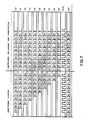
filter 10 was implemented using Signetics Corporation's 2 micron double metal standard cell technology. The current chip has ten taps. The IC lay out was performed using Silver Lisco's CAL-MP software. We will now present the simulation results of the various modes of operation of the chip. - Referring to the coefficient loading procedure of Figure 7 and Table 2, we desire our filter coefficients to be as listed in Table 1. In Figure 7, we have used the decimal equivalents of Table 1 for clarity. We presented the coefficients to the C-
IN bus 14 through the C-I/O gates 41 in reverse fashion and at the end of ten clock pulses we can see that they are in the correct C-REG's 32. As mentioned earlier, for loading coefficients the C-RW 42 signal is set to 1. - Now for the verification of our loading the C-
RW 42 signal is set to 0 and we again apply ten coefficient clock pulses. The coefficient verification and reloading portion of Figure 7 and Table 2 show that all of the coefficients appeared at the C-I/O gates 44 via C-OUT bus 15 (in reverse order) and are reloaded into the C-REG's 32 via C-IN bus 14. This concludes the simulation of our initialization procedure. - For normal operation, the coefficient clock CLK-C enable signal (CEN) is set to 1. Since, once initialization of the filter has been successfully accomplished, we do not want the coefficients to change, this signal is an added protection against a stray coefficient clock pulse (CLK-C) altering the coefficients. Data is presented via the D-
IN bus 12 and the normal operation clock (CLK-N) now becomes the only system clock and filtering is performed on the data. - We have successfully simulated the filter using various coefficients and random data.


Claims (16)
means to receive and store a plurality of coefficients, one coefficient per tap, wherein each coefficient is an integer power of 2;
means to receive and shift a data input word in each of said taps, the extent of said shift being determined by the value of said coefficient stored in said tap;
said shifted data word being equivalent to the product of said input data word and said coefficient of said tap;
means to add said product to the delayed output of the previous tap to form the cumulative sum of the products of all previous taps;
means to delay and forward said cumulative sum to the next tap, and
means to output the cumulative sum of all taps in said filter.
input means to load said coefficients into said filter in an initialization phase;
a coefficient bus to transport each of said coefficients to its destination tap; and
a coefficient register at each tap to store the coefficient for said tap.
said coefficient bus is a serial bus;
said coefficient registers are connected to each other in a serial chain; and
said coefficients are loaded such that the last coefficient in the chain is loaded first and each coeffi cient is shifted down said chain in inverse relationship to tis proximity to the start of said chain.
said coefficient bus is a bidirectional bus;
means to reverse the direction of serial bit flow on said coefficient bus;
output terminal means on said coefficient bus; and
means to verify the loading of said coefficients by reading them out serially to said output terminal means when said bus direction is reversed and reloading said coefficients in said destination taps.
a data bus connected to each of said taps,
whereby said data input words are broadcast to each of said taps;
a shifter in each of said taps in the form of a NAND-NAND multiplexer connected to said data bus and to said coefficient register of said tap which receives each data word sequentially and shifts its bits according to said coefficient stored in said coefficient register, the output of said shifter being a weighted data sample.
means to expand the length of said filter by cascading stages of said filter.
a sum-in bus which transports the cumulative sum of previous weighted data sample to each tap;
an adder to add the output of said shifter of each tap to said cumulative sum;
a delay element;
a sum-out bus which transports the sum of said adder to said delay element, said delay element connected to the sum-in bus of the next tap.
a shifter having an input section comprising eight first sets of NAND gates, each set receiving all eight bits of said data word;
a selection line from said coefficient register to each of said first sets of NAND gates, said coefficient determining which selection line is active;
a second set of NAND gates to receive the output of the selected first set of NAND gates, the combination of the two sets of NAND gates providing the required shift as a shifter;
a set of EXOR gates at the output of said shifter to perform one's complement conversion on the output of said shifter, which output is latched for transfer to said adder.
Applications Claiming Priority (4)
| Application Number | Priority Date | Filing Date | Title |
|---|---|---|---|
| US06/923,534 US4791597A (en) | 1986-10-27 | 1986-10-27 | Multiplierless FIR digital filter with two to the Nth power coefficients |
| US923534 | 1986-10-27 | ||
| US944295 | 1986-12-18 | ||
| US06/944,295 US4782458A (en) | 1986-12-18 | 1986-12-18 | Architecture for power of two coefficient FIR filter |
Publications (3)
| Publication Number | Publication Date |
|---|---|
| EP0266004A2 true EP0266004A2 (en) | 1988-05-04 |
| EP0266004A3 EP0266004A3 (en) | 1989-11-29 |
| EP0266004B1 EP0266004B1 (en) | 1994-01-12 |
Family
ID=27129871
Family Applications (1)
| Application Number | Title | Priority Date | Filing Date |
|---|---|---|---|
| EP19870202045 Expired - Lifetime EP0266004B1 (en) | 1986-10-27 | 1987-10-26 | Architecture for power of two coefficient fir filter |
Country Status (2)
| Country | Link |
|---|---|
| EP (1) | EP0266004B1 (en) |
| DE (1) | DE3788779T2 (en) |
Cited By (7)
| Publication number | Priority date | Publication date | Assignee | Title |
|---|---|---|---|---|
| US5479363A (en) * | 1993-04-30 | 1995-12-26 | The Regents Of The University Of California | Programmable digital signal processor using switchable unit-delays for optimal hardware allocation |
| WO1997009780A1 (en) * | 1995-09-07 | 1997-03-13 | Philips Electronics N.V. | Improved digital filter |
| FR2739991A1 (en) * | 1995-10-13 | 1997-04-18 | Ricoh Kk | IIR digital filter |
| EP1052845A2 (en) * | 1999-05-12 | 2000-11-15 | NuCore Technology Inc. | Image processing apparatus |
| CN102931945A (en) * | 2012-11-26 | 2013-02-13 | 昆山北极光电子科技有限公司 | Method for automatically realizing bandpass digital filtering |
| US11521047B1 (en) * | 2018-04-20 | 2022-12-06 | Brown University | Deep neural network |
| CN116827308A (en) * | 2023-08-24 | 2023-09-29 | 上海力通通信有限公司 | Resource optimization type FIR filter and implementation method thereof |
Citations (1)
| Publication number | Priority date | Publication date | Assignee | Title |
|---|---|---|---|---|
| DE3230030A1 (en) * | 1981-08-14 | 1983-03-03 | RCA Corp., 10020 New York, N.Y. | DIGITAL FIR FILTER |
-
1987
- 1987-10-26 DE DE19873788779 patent/DE3788779T2/en not_active Expired - Fee Related
- 1987-10-26 EP EP19870202045 patent/EP0266004B1/en not_active Expired - Lifetime
Patent Citations (1)
| Publication number | Priority date | Publication date | Assignee | Title |
|---|---|---|---|---|
| DE3230030A1 (en) * | 1981-08-14 | 1983-03-03 | RCA Corp., 10020 New York, N.Y. | DIGITAL FIR FILTER |
Non-Patent Citations (2)
| Title |
|---|
| 1974 INTERNATIONAL CONFERENCE ON COMMUNICATIONS, Minneapolis, Minnesota, 17th - 19th June 1974, pages 18D-1/4, IEEE, New York, US; A. TOMOZAWA: "Nonrecursive digital filters with coefficients of powers of two" * |
| FERNSEH-UND KINO TECHNIK, vol. 39, no. 1, January 1985, pages 15-19, Heidelberg, DE; P. DRAHEIM: "Digitale Filter f}r die Videosignalverarbeitung in Gate-Array-Technik" * |
Cited By (10)
| Publication number | Priority date | Publication date | Assignee | Title |
|---|---|---|---|---|
| US5479363A (en) * | 1993-04-30 | 1995-12-26 | The Regents Of The University Of California | Programmable digital signal processor using switchable unit-delays for optimal hardware allocation |
| WO1997009780A1 (en) * | 1995-09-07 | 1997-03-13 | Philips Electronics N.V. | Improved digital filter |
| FR2739991A1 (en) * | 1995-10-13 | 1997-04-18 | Ricoh Kk | IIR digital filter |
| EP1052845A2 (en) * | 1999-05-12 | 2000-11-15 | NuCore Technology Inc. | Image processing apparatus |
| EP1052845A3 (en) * | 1999-05-12 | 2002-08-07 | NuCore Technology Inc. | Image processing apparatus |
| US6819717B1 (en) | 1999-05-12 | 2004-11-16 | Nucore Technology, Inc. | Image processing apparatus |
| CN102931945A (en) * | 2012-11-26 | 2013-02-13 | 昆山北极光电子科技有限公司 | Method for automatically realizing bandpass digital filtering |
| US11521047B1 (en) * | 2018-04-20 | 2022-12-06 | Brown University | Deep neural network |
| CN116827308A (en) * | 2023-08-24 | 2023-09-29 | 上海力通通信有限公司 | Resource optimization type FIR filter and implementation method thereof |
| CN116827308B (en) * | 2023-08-24 | 2023-11-24 | 上海力通通信有限公司 | Resource optimization type FIR filter and implementation method thereof |
Also Published As
| Publication number | Publication date |
|---|---|
| DE3788779T2 (en) | 1994-06-30 |
| EP0266004A3 (en) | 1989-11-29 |
| DE3788779D1 (en) | 1994-02-24 |
| EP0266004B1 (en) | 1994-01-12 |
Similar Documents
| Publication | Publication Date | Title |
|---|---|---|
| US4862402A (en) | Fast multiplierless architecture for general purpose VLSI FIR digital filters with minimized hardware | |
| US6163788A (en) | Programmable finite impulse response processor with scalable dynamic data range | |
| US5287299A (en) | Method and apparatus for implementing a digital filter employing coefficients expressed as sums of 2 to an integer power | |
| US6584481B1 (en) | FPGA implemented bit-serial multiplier and infinite impulse response filter | |
| US5500811A (en) | Finite impulse response filter | |
| US4782458A (en) | Architecture for power of two coefficient FIR filter | |
| EP0372350B1 (en) | Programmable digital filter | |
| JPS63160406A (en) | Non-circulating type limited impulse response digital filter | |
| US5479363A (en) | Programmable digital signal processor using switchable unit-delays for optimal hardware allocation | |
| US4802111A (en) | Cascadable digital filter processor employing moving coefficients | |
| US4947363A (en) | Pipelined processor for implementing the least-mean-squares algorithm | |
| EP0150114B1 (en) | Sampled data fir filters with enhanced tap weight resolution | |
| US3988606A (en) | Digital filter device for processing binary-coded signal samples | |
| US6370556B1 (en) | Method and arrangement in a transposed digital FIR filter for multiplying a binary input signal with tap coefficients and a method for designing a transposed digital filter | |
| EP0266004B1 (en) | Architecture for power of two coefficient fir filter | |
| JPH082014B2 (en) | Multi-stage digital filter | |
| Yazhini et al. | Fir filter implementation using modified distributed arithmetic architecture | |
| JP3318753B2 (en) | Product-sum operation device and product-sum operation method | |
| Moeller et al. | Field programmable gate array based radar front-end digital signal processing | |
| US5781462A (en) | Multiplier circuitry with improved storage and transfer of booth control coefficients | |
| EP0564751B1 (en) | High-resolution digital filter | |
| US4584563A (en) | Method of residue to analog conversion | |
| Ramesh et al. | Implementation and Design of FIR Filters using Verilog HDL and FPGA | |
| JPH0575394A (en) | Digital filter and digital signal processing system | |
| Rainer et al. | Adder-based digital signal processor architecture for 80 ns cycle time |
Legal Events
| Date | Code | Title | Description |
|---|---|---|---|
| PUAI | Public reference made under article 153(3) epc to a published international application that has entered the european phase |
Free format text: ORIGINAL CODE: 0009012 |
|
| AK | Designated contracting states |
Kind code of ref document: A2 Designated state(s): DE FR GB IT |
|
| PUAL | Search report despatched |
Free format text: ORIGINAL CODE: 0009013 |
|
| AK | Designated contracting states |
Kind code of ref document: A3 Designated state(s): DE FR GB IT |
|
| 17P | Request for examination filed |
Effective date: 19900523 |
|
| 17Q | First examination report despatched |
Effective date: 19930218 |
|
| GRAA | (expected) grant |
Free format text: ORIGINAL CODE: 0009210 |
|
| AK | Designated contracting states |
Kind code of ref document: B1 Designated state(s): DE FR GB IT |
|
| REF | Corresponds to: |
Ref document number: 3788779 Country of ref document: DE Date of ref document: 19940224 |
|
| ITF | It: translation for a ep patent filed |
Owner name: ING. C. GREGORJ S.P.A. |
|
| ET | Fr: translation filed | ||
| PLBE | No opposition filed within time limit |
Free format text: ORIGINAL CODE: 0009261 |
|
| STAA | Information on the status of an ep patent application or granted ep patent |
Free format text: STATUS: NO OPPOSITION FILED WITHIN TIME LIMIT |
|
| 26N | No opposition filed | ||
| ITPR | It: changes in ownership of a european patent |
Owner name: CAMBIO RAGIONE SOCIALE;PHILIPS ELECTRONICS N.V. |
|
| REG | Reference to a national code |
Ref country code: FR Ref legal event code: CD |
|
| PGFP | Annual fee paid to national office [announced via postgrant information from national office to epo] |
Ref country code: GB Payment date: 19960930 Year of fee payment: 10 |
|
| PGFP | Annual fee paid to national office [announced via postgrant information from national office to epo] |
Ref country code: FR Payment date: 19961022 Year of fee payment: 10 |
|
| PGFP | Annual fee paid to national office [announced via postgrant information from national office to epo] |
Ref country code: DE Payment date: 19961218 Year of fee payment: 10 |
|
| PG25 | Lapsed in a contracting state [announced via postgrant information from national office to epo] |
Ref country code: GB Free format text: LAPSE BECAUSE OF NON-PAYMENT OF DUE FEES Effective date: 19971026 |
|
| PG25 | Lapsed in a contracting state [announced via postgrant information from national office to epo] |
Ref country code: FR Free format text: THE PATENT HAS BEEN ANNULLED BY A DECISION OF A NATIONAL AUTHORITY Effective date: 19971031 |
|
| GBPC | Gb: european patent ceased through non-payment of renewal fee |
Effective date: 19971026 |
|
| PG25 | Lapsed in a contracting state [announced via postgrant information from national office to epo] |
Ref country code: DE Free format text: LAPSE BECAUSE OF NON-PAYMENT OF DUE FEES Effective date: 19980701 |
|
| REG | Reference to a national code |
Ref country code: FR Ref legal event code: ST |
|
| PG25 | Lapsed in a contracting state [announced via postgrant information from national office to epo] |
Ref country code: IT Free format text: LAPSE BECAUSE OF NON-PAYMENT OF DUE FEES;WARNING: LAPSES OF ITALIAN PATENTS WITH EFFECTIVE DATE BEFORE 2007 MAY HAVE OCCURRED AT ANY TIME BEFORE 2007. THE CORRECT EFFECTIVE DATE MAY BE DIFFERENT FROM THE ONE RECORDED. Effective date: 20051026 |