EP0265584A2 - Method and materials for etching silicon dioxide using silicon nitride or silicon rich dioxide as an etch barrier - Google Patents
Method and materials for etching silicon dioxide using silicon nitride or silicon rich dioxide as an etch barrier Download PDFInfo
- Publication number
- EP0265584A2 EP0265584A2 EP87106471A EP87106471A EP0265584A2 EP 0265584 A2 EP0265584 A2 EP 0265584A2 EP 87106471 A EP87106471 A EP 87106471A EP 87106471 A EP87106471 A EP 87106471A EP 0265584 A2 EP0265584 A2 EP 0265584A2
- Authority
- EP
- European Patent Office
- Prior art keywords
- silicon
- silicon dioxide
- layer
- etching
- dioxide
- Prior art date
- Legal status (The legal status is an assumption and is not a legal conclusion. Google has not performed a legal analysis and makes no representation as to the accuracy of the status listed.)
- Withdrawn
Links
Images

Classifications
-
- H—ELECTRICITY
- H01—ELECTRIC ELEMENTS
- H01L—SEMICONDUCTOR DEVICES NOT COVERED BY CLASS H10
- H01L21/00—Processes or apparatus adapted for the manufacture or treatment of semiconductor or solid state devices or of parts thereof
- H01L21/02—Manufacture or treatment of semiconductor devices or of parts thereof
- H01L21/04—Manufacture or treatment of semiconductor devices or of parts thereof the devices having at least one potential-jump barrier or surface barrier, e.g. PN junction, depletion layer or carrier concentration layer
- H01L21/18—Manufacture or treatment of semiconductor devices or of parts thereof the devices having at least one potential-jump barrier or surface barrier, e.g. PN junction, depletion layer or carrier concentration layer the devices having semiconductor bodies comprising elements of Group IV of the Periodic System or AIIIBV compounds with or without impurities, e.g. doping materials
- H01L21/30—Treatment of semiconductor bodies using processes or apparatus not provided for in groups H01L21/20 - H01L21/26
- H01L21/31—Treatment of semiconductor bodies using processes or apparatus not provided for in groups H01L21/20 - H01L21/26 to form insulating layers thereon, e.g. for masking or by using photolithographic techniques; After treatment of these layers; Selection of materials for these layers
- H01L21/3105—After-treatment
- H01L21/311—Etching the insulating layers by chemical or physical means
- H01L21/31105—Etching inorganic layers
- H01L21/31111—Etching inorganic layers by chemical means
- H01L21/31116—Etching inorganic layers by chemical means by dry-etching
Definitions
- the present invention relates to etching processes and materials and more particularly to an etching process and and etch stop structure for directionally etching silicon dioxide with high selectivity to an etch stop consisting of silicon nitride or silicon rich silicon dioxide.
- U.S. Patent 4,427,516 issued January 24, 1984 to Levinstein et al, entitled APPARATUS AND METHOD FOR PLASMA-ASSISTED ETCHING OF WAFERS teaches a plasma-assisted etching apparatus and method designed to pattern silicon dioxide in a plasma derived from a mixture of trifluoromethane and ammonia wherein surfaces in the reaction chamber are coated with a layer of silicon. Contamination of wafers during the etching process is thereby substantially reduced.
- U.S. Patent 4,376,672 issued March 15, 1983 to Wang et al describes a method for etching a layer of inorganic insulating material formed on a semiconductor wafer and containing silicon as the principal metallic element.
- the method involves disposing a wafer on one of a pair of electrode structures in a closed chamber.
- a reactive gas mixture comprising principally a fluorocarbon gas doped with a preselected quantity of carbon dioxide is supplied to the chamber.
- Radio frequency electrical energy is suppled to one of the electrode structures to create a plasma of the reactive gas mixture for chemically attacking the insulating material.
- U.S. Patent 4,431,477 issued February 14, 1984 to Zajao entitled PLASMA ETCHING WITH NITROUS OXIDE AND FLUORO COMPOUND GAS MIXTURE discloses a process for use in the manufacture of multilayer thin film integrated circuits for selective removal of specific layers, and a composition of matter useful in the process for selective etching of polysilicon and silicon nitrides during the manufacture of thin film integrated circuits.
- a multilayer thin film integrated circuit is exposed to a plasma formed from a gaseous mixture of nitrous oxide and a fluoro compound.
- the nitrous oxide preferably comprises between 2.5% and 9.0% of the mixture and the fluoro compound preferably comprises between 91.0% and 97.5% of the mixture.
- U.S. Patent 4,490,205 issued December 25, 1984 to Hartman entitled PLASMA ETCHING USING HYDROGEN BROMIDE ADDITION relates to a plasma etch chemistry which allows a near perfectly anisotropic etch of silicon.
- a Cl-containing compound such as HC1 has HBr added thereto, readily allowing the anisotropic etching of silicon. This is due to the low vola- tilit y of SiBr 4 .
- the silicon surface facing the discharge is subjected to ion bombardment, allowing the volatization (etching) of silicon as a Si-Cl-Br compound.
- the Br which absorbs on the sidewalls of the etched silicon passivates them from the etching.
- U.S. Patent 4,431,477 discusses the use of Freon 13 with nitrous oxide to etch nitride at a faster rate than oxide. This is in contrast to the present inven- 'tion wherein nitride is caused to etch significantly slower than oxide.
- U.S. Patent 4,376,672 and 4,283,249 discuss selective etching of oxide and nitride to silicon. In both cases, only silicon can be used as an etching barrier.
- U.S. Patent 4,490,209 claims selective etching of silicon to nitride. Although nitride is used as an etching barrier, the applications of patterning silicon are generally quite different trom that of defining an oxide layer. The features of the present invention are unique in that selectivity is obtained between two dielectric materials, silicon dioxide and nitride wherein oxide etches considerably faster than nitride in this process.
- CCIF 3 + H 2 will etch SiO 2 directionally with high selectivity to Si 3 N 4 and silicon rich Si0 2 . It has also been shown in the prior art that the use of a dielectric material as an etch stop prevents the transfer ot topography into underlaying layers of wafer material such as an SiO 2 film used as isolation.
- An object of the present invention is to provide a process for etching SiO 2 using either silicon rich SiO 2 or Si 3 N 4 as an etching barrier over a substrate.
- Another object of the present invention is to provide an etching process wherein selectivity is obtained between two dielectric materials, silicon dioxide and nitride or silicon dioxide and silicon rich silicon dioxide wherein the oxide etches considerably faster than nitride or silicon rich silicon dioxide because of the selectivity of oxide to nitride.
- a further object of the present invention is to provide an etching process wherein silicon dioxide on a substrate is directionally etched in a fluorocarbon gas to form silicon dioxide spacers on a substrate, and wherein the substrate surface is protected by an etch stop composed of silicon nitride or silicon rich silicon dioxide.
- the process of the present invention includes etching, for example, reactive ion etching.
- etching for example, reactive ion etching.
- means for carrying out the reactive ion etching is available in the art, and does not form a separate portion of the present invention, a typical reactive ion etching structure will be described to provide a complete disclosure.
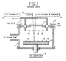
- FIG. 1 A typical reactive ion etching systemis shown in FIG. 1 including a support means 10 for mounting recessed work specimens within an enclosed vacuum chamber 14.
- the work specimens are disposed between a pair of electrodes 12,16 which are energized with radio frequency power from R.F. generator 18 to produce an electric field for ionizing a gas which is introduced through inlets 20.
- Control of the etching process is maintained by directing a laser beam from laser 22 through window 24 and which is reflected from the specimen surface to a thickness measurement means 26.
- the etching of the silicon dioxide material is carried out by an etch gas consisting ot CClF 3 + H 2 , and more particularly thirty percent 20 millitorr CClF 3 plus seventy percent H2with a power density of 0.35 watts/cm 2 in a 7, 82 mm wafer reactive ion etch system.
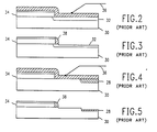
- FIG. 2 an illustration is provided showing a prior art example of an etch process for forming a silicon dioxide spacer sidewall.
- a substrate 30, such as silicon or gallium arsenide contains a shallow doped junction region 32 and a polysilicon layer 34.
- a layer of silicon dioxide 36 is tormed on the polysilicon 34 and junction 32, for example, by chemical vapor deposition.
- the structure is reactive ion etched in a system as shown in FIG. 1. The etching is directional normal to the structure surface such that a silicon dioxide sidewall 38 remains, as shown in FIG. 3.
- FIG. 4 another embodiment of a structure is shown including a semi-recessed oxide region 28 rather than a shallow junction. The remainder of the structure of FIG. 4 is the same as shown in FIG. 2.
- FIG. 4 is directionally reactively ion etched in the system of FIG. 1 to remove the silicon dioxide layer 36 and provide sidewall spacer 38 as shown in FIG. 5. However, a significant portion ot the semi-recessed oxide region 28 is also removed during the etching process, to the detriment of the resultant device structure.
- FIG. 6 an illustration of curves showing the etch rates of silicon dioxide, silicon nitride and silicon in CClF 3 + H 2 is depicted.
- the etch rate of silicon dioxide is shown to be higher than silicon nitride and silicon, with the differences between the etch rates becoming larger as the percentage of H 2 in the gas mixture increases to seventy percent (+7 percent):
- the application of this etch rate difference is used in the etch barrier structure of the prqcess of the present invention.
- the silicon nitride and the silicon rich silicon dioxide (that is, having a very high silicon content, for example, forty percent silicon in the silicon dioxide compound) etch more slowly than normal silicon dioxide may be a result of the CC1F 3 +H 2 etching gas being highly selective to silicon, in the order of 70 to 80 to 1.
- the silicon nitride which is composed of about 43% Si as opposed to silicon dioxide which is composed of about 33% Si, etches more slowly than the silicon dioxide.
- silicon rich Si0 2 which has a much higher silicon content than regular Si0 2 .
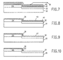
- FIGS. 7, 8 and 9 the process of the present invention is shown for fabricating a silicon dioxide sidewall spacer and a structure containing a shallow doped junction similar to the structure of FIGS. 2 and 3.
- the substrate 30 contains a shallow doped junction 32 and a polysilicon layer 34.
- An etch barrier 40 is deposited on the surface of the structure. If the substrate 30 is single crystal silicon, and if the etch barrier 40 is composed of silicon nitride, normal practice requires a thin passivating layer 42 of silicon dioxide to be placed between the nitride and the silicon to prevent defect formation. If the etch barrier is silicon rich silicon dioxide, such passivating layer 42 is not needed. Likewise, the passivating layer 42 may be unnecessary if the substrate 30 is composed of gallium arsenide.
- a layer of silicon dioxide 36 insulating material is then deposited on the surface of the structure as described for FIG. 2.
- the structure is then directionally etched in the system of FIG. 1 to provide the sidewall spacer 38 in FIG. 8.
- the silicon nitride etches slower than the silicon dioxide, when the sidewall is completed, there is still a thickness of silicon nitride etch barrier protecting the surtace of the shallow junction.
- the structure is reactively ion etched using CF 4 as the etching gas to remove the nitride layer 40. If a passivating layer 42 is used, it is removed by using a wet etching with a buftered HF solution which has infinite selectivity to silicon and, therefore, no junction material is removed as shown in FIG. 10.
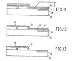
- FIGS. 11, 12 and 13 illustrate the use ot a barrier layer according to the present invention in a process for forming a sidewall on a structure including semi-recessed oxide.
- a substrate 30 is provided having a semi-recessed oxide region 28 therein, and a layer of polysilicon 34 similar to the structure of FIG. 4.
- a silicon nitride etch barrier layer is tormed and, if necessary, a thin silicon dioxide passivating layer 42 is first deposited on the structure surface.
- FIG. 12 illustrates the first process step, which is the same as described for FIG. 8, wherein a directional reactive ion etch is performed to remove the silicon dioxide layer 36 with the exception of the remaining sidewall 38.
- the nitride layer 40 is removed by reactive ion etching in CF 4 similar to the step of FIG. 9 and, if present, the passivating silicon dioxide layer 42 is also removed by reactive ion etching in CF 4 .
Abstract
Description
- The present invention relates to etching processes and materials and more particularly to an etching process and and etch stop structure for directionally etching silicon dioxide with high selectivity to an etch stop consisting of silicon nitride or silicon rich silicon dioxide.
- In U.S. Patent 4,324,611 issued April 13, 1982 to Vogel et al, entitled PROCESS AND GAS MIXTURE FOR ETCHING SILICON DIOXIDE AND SILICON NITRIDE, a process and gas mixture for etching silicon dioxide and/or silicon nitride in a plasma environment in a planar reactor is described. The gas mixture comprises a primary etching gas and a secondary gas which controls the selectivity of the etch. The process is carried out at relatively.high pressure and power levels and provides substantially fast removal of silicon dioxide and/or silicon nitride.
- U.S. Patent 4,427,516 issued January 24, 1984 to Levinstein et al, entitled APPARATUS AND METHOD FOR PLASMA-ASSISTED ETCHING OF WAFERS teaches a plasma-assisted etching apparatus and method designed to pattern silicon dioxide in a plasma derived from a mixture of trifluoromethane and ammonia wherein surfaces in the reaction chamber are coated with a layer of silicon. Contamination of wafers during the etching process is thereby substantially reduced.
- U.S. Patent 4,376,672 issued March 15, 1983 to Wang et al describes a method for etching a layer of inorganic insulating material formed on a semiconductor wafer and containing silicon as the principal metallic element. The method involves disposing a wafer on one of a pair of electrode structures in a closed chamber. A reactive gas mixture comprising principally a fluorocarbon gas doped with a preselected quantity of carbon dioxide is supplied to the chamber.
- Radio frequency electrical energy is suppled to one of the electrode structures to create a plasma of the reactive gas mixture for chemically attacking the insulating material.
- U.S. Patent 4,431,477 issued February 14, 1984 to Zajao entitled PLASMA ETCHING WITH NITROUS OXIDE AND FLUORO COMPOUND GAS MIXTURE discloses a process for use in the manufacture of multilayer thin film integrated circuits for selective removal of specific layers, and a composition of matter useful in the process for selective etching of polysilicon and silicon nitrides during the manufacture of thin film integrated circuits. A multilayer thin film integrated circuit is exposed to a plasma formed from a gaseous mixture of nitrous oxide and a fluoro compound. The nitrous oxide preferably comprises between 2.5% and 9.0% of the mixture and the fluoro compound preferably comprises between 91.0% and 97.5% of the mixture.
- In U.S. Patent 4,283,249 entitled REACTIVE ION ETCHING issued August 11, 1981 to Ephrath, a process is described wherein a silicon oxide, nitride and/or oxynitride surface on a substrate is selectively etched at a rate greater than that of the substrate by a reactive ion etching employing a gaseous mixture containing a fluorocarbon and a second gas capable of supplying hydrogen.
- U.S. Patent 4,490,205 issued December 25, 1984 to Hartman entitled PLASMA ETCHING USING HYDROGEN BROMIDE ADDITION relates to a plasma etch chemistry which allows a near perfectly anisotropic etch of silicon. A Cl-containing compound such as HC1 has HBr added thereto, readily allowing the anisotropic etching of silicon. This is due to the low vola- tility of SiBr4. The silicon surface facing the discharge is subjected to ion bombardment, allowing the volatization (etching) of silicon as a Si-Cl-Br compound. The Br which absorbs on the sidewalls of the etched silicon passivates them from the etching.
- The present invention is distinct from the described prior art. In particular, U.S. Patent 4,431,477 discusses the use of Freon 13 with nitrous oxide to etch nitride at a faster rate than oxide. This is in contrast to the present inven- 'tion wherein nitride is caused to etch significantly slower than oxide.
- U.S. Patent 4,376,672 and 4,283,249 discuss selective etching of oxide and nitride to silicon. In both cases, only silicon can be used as an etching barrier. U.S. Patent 4,490,209 claims selective etching of silicon to nitride. Although nitride is used as an etching barrier, the applications of patterning silicon are generally quite different trom that of defining an oxide layer. The features of the present invention are unique in that selectivity is obtained between two dielectric materials, silicon dioxide and nitride wherein oxide etches considerably faster than nitride in this process.
- It is known that CCIF3 + H2 will etch SiO2 directionally with high selectivity to Si3N4 and silicon rich Si02. It has also been shown in the prior art that the use of a dielectric material as an etch stop prevents the transfer ot topography into underlaying layers of wafer material such as an SiO2 film used as isolation.
- An object of the present invention is to provide a process for etching SiO2 using either silicon rich SiO2 or Si3N4 as an etching barrier over a substrate.
- Another object of the present invention is to provide an etching process wherein selectivity is obtained between two dielectric materials, silicon dioxide and nitride or silicon dioxide and silicon rich silicon dioxide wherein the oxide etches considerably faster than nitride or silicon rich silicon dioxide because of the selectivity of oxide to nitride.
- A further object of the present invention is to provide an etching process wherein silicon dioxide on a substrate is directionally etched in a fluorocarbon gas to form silicon dioxide spacers on a substrate, and wherein the substrate surface is protected by an etch stop composed of silicon nitride or silicon rich silicon dioxide.
- The foregoing and other objects features and advantages of the invention will be apparent from the following more particular description of the invention as illustrated in the accompanying drawings.
-
- FIG. 1 is a schematic illustration of'a typical reactive ion etching system used to carry out the etching process of the present invention.
- FIG. 2 is a schematic illustration of an embodiment of a semiconductor structure with a shallow junction therein showing a layer of silicon dioxide thereon which is to be etched to form a sidewall spacer.
- FIG. 3 is a schematic illustration of the structure of FIG. 2 at the completion of the etch process showing how the prior art etch process may remove a portion of a doped shallow junction.
- FIG. 4 is a schematic illustration of another embodiment of a structure with a semi-recessed oxide showing a layer of silicon dioxide thereon which is to be etched to form a sidewall spacer.
- FIG. 5 is a schematic illustration of the embodiment of FIG. 4 at the completion of the etch process showing how the prior art etch process may remove a portion of the semi-recessed oxide.
- FIG. 6 is an illustration showing the etch rates of silicon dioxide, silicon nitride and silicon within CClF3+H2 etch gas of different hydrogen percentages.
- FIG. 7 is a schematic illustration of a semiconductor structure with a shallow junction therein showing a layer of silicon dioxide over an etch barrier according to the principles of the present invention.
- FIG. 8 is a schematic illustration of the structure of FIG. 7 at the completion of the etching of the silicon dioxide to form a sidewall spacer with the substrate protected by an etch barrier according to the principles of the present invention.
- FIGS. 9 and 10 are schematic illustrations of the structure of FIG. 7 showing the removal of the etch barrier.
- FIGS. 11, 12 and 13 are schematic illustrations of an embodiment of a semiconductor structure with a semi-recessed oxide isolation region therein showing steps of an etch process employing an etch barrier according to the principles of the present invention.
- The process of the present invention includes etching, for example, reactive ion etching. Although the means for carrying out the reactive ion etching is available in the art, and does not form a separate portion of the present invention, a typical reactive ion etching structure will be described to provide a complete disclosure.
- A typical reactive ion etching systemis shown in FIG. 1 including a support means 10 for mounting recessed work specimens within an enclosed
vacuum chamber 14. The work specimens are disposed between a pair ofelectrodes generator 18 to produce an electric field for ionizing a gas which is introduced throughinlets 20. Control of the etching process is maintained by directing a laser beam fromlaser 22 throughwindow 24 and which is reflected from the specimen surface to a thickness measurement means 26. - In the present invention, the etching of the silicon dioxide material is carried out by an etch gas consisting ot CClF3 + H2, and more particularly thirty
percent 20 millitorr CClF3 plus seventy percent H2with a power density of 0.35 watts/cm2 in a 7, 82 mm wafer reactive ion etch system. - Referring now to FIG. 2, an illustration is provided showing a prior art example of an etch process for forming a silicon dioxide spacer sidewall. A
substrate 30, such as silicon or gallium arsenide contains a shallowdoped junction region 32 and apolysilicon layer 34. A layer ofsilicon dioxide 36 is tormed on thepolysilicon 34 andjunction 32, for example, by chemical vapor deposition. The structure is reactive ion etched in a system as shown in FIG. 1. The etching is directional normal to the structure surface such that asilicon dioxide sidewall 38 remains, as shown in FIG. 3. - It has been observed, that even with silicon selectivity etch, a portion of the surtace of the doped junctions is etched away before the etch process can be halted. However, even it as little as 100 Angstroms of the doped shallow junction is removed, it will have detrimental effects on the resultant structure.
- Referring to FIG. 4, another embodiment of a structure is shown including a
semi-recessed oxide region 28 rather than a shallow junction. The remainder of the structure of FIG. 4 is the same as shown in FIG. 2. - The structure of FIG. 4 is directionally reactively ion etched in the system of FIG. 1 to remove the
silicon dioxide layer 36 and providesidewall spacer 38 as shown in FIG. 5. However, a significant portion ot thesemi-recessed oxide region 28 is also removed during the etching process, to the detriment of the resultant device structure. - Referring next to FIG. 6, an illustration of curves showing the etch rates of silicon dioxide, silicon nitride and silicon in CClF3 + H2 is depicted. At a pressure of 25 millitorr and a gas flow rate of 135 sccm the etch rate of silicon dioxide is shown to be higher than silicon nitride and silicon, with the differences between the etch rates becoming larger as the percentage of H2 in the gas mixture increases to seventy percent (+7 percent): The application of this etch rate difference is used in the etch barrier structure of the prqcess of the present invention.
- The fact that the silicon nitride and the silicon rich silicon dioxide (that is, having a very high silicon content, for example, forty percent silicon in the silicon dioxide compound) etch more slowly than normal silicon dioxide may be a result of the CC1F3+H2 etching gas being highly selective to silicon, in the order of 70 to 80 to 1. Thus, the silicon nitride, which is composed of about 43% Si as opposed to silicon dioxide which is composed of about 33% Si, etches more slowly than the silicon dioxide. The same is true of silicon rich Si02 which has a much higher silicon content than regular Si02.
- Referring to FIGS. 7, 8 and 9, the process of the present invention is shown for fabricating a silicon dioxide sidewall spacer and a structure containing a shallow doped junction similar to the structure of FIGS. 2 and 3.
- In FIG 7, the
substrate 30 contains a shallow dopedjunction 32 and apolysilicon layer 34. Anetch barrier 40 is deposited on the surface of the structure. If thesubstrate 30 is single crystal silicon, and if theetch barrier 40 is composed of silicon nitride, normal practice requires athin passivating layer 42 of silicon dioxide to be placed between the nitride and the silicon to prevent defect formation. If the etch barrier is silicon rich silicon dioxide,such passivating layer 42 is not needed. Likewise, thepassivating layer 42 may be unnecessary if thesubstrate 30 is composed of gallium arsenide. - A layer of
silicon dioxide 36 insulating material is then deposited on the surface of the structure as described for FIG. 2. - The structure is then directionally etched in the system of FIG. 1 to provide the
sidewall spacer 38 in FIG. 8. However, because the silicon nitride etches slower than the silicon dioxide, when the sidewall is completed, there is still a thickness of silicon nitride etch barrier protecting the surtace of the shallow junction. - In FIG. 9, the structure is reactively ion etched using CF4 as the etching gas to remove the
nitride layer 40. If apassivating layer 42 is used, it is removed by using a wet etching with a buftered HF solution which has infinite selectivity to silicon and, therefore, no junction material is removed as shown in FIG. 10. - FIGS. 11, 12 and 13 illustrate the use ot a barrier layer according to the present invention in a process for forming a sidewall on a structure including semi-recessed oxide.
- In FIG. 11, a
substrate 30 is provided having asemi-recessed oxide region 28 therein, and a layer ofpolysilicon 34 similar to the structure of FIG. 4. - As described for FIG. 7, a silicon nitride etch barrier layer is tormed and, if necessary, a thin silicon
dioxide passivating layer 42 is first deposited on the structure surface. - FIG. 12 illustrates the first process step, which is the same as described for FIG. 8, wherein a directional reactive ion etch is performed to remove the
silicon dioxide layer 36 with the exception of the remainingsidewall 38. - In FIG. 13, the
nitride layer 40 is removed by reactive ion etching in CF4 similar to the step of FIG. 9 and, if present, the passivatingsilicon dioxide layer 42 is also removed by reactive ion etching in CF4.
Claims (8)
Applications Claiming Priority (2)
| Application Number | Priority Date | Filing Date | Title |
|---|---|---|---|
| US92471186A | 1986-10-30 | 1986-10-30 | |
| US924711 | 1986-10-30 |
Publications (2)
| Publication Number | Publication Date |
|---|---|
| EP0265584A2 true EP0265584A2 (en) | 1988-05-04 |
| EP0265584A3 EP0265584A3 (en) | 1989-12-06 |
Family
ID=25450595
Family Applications (1)
| Application Number | Title | Priority Date | Filing Date |
|---|---|---|---|
| EP87106471A Withdrawn EP0265584A3 (en) | 1986-10-30 | 1987-05-05 | Method and materials for etching silicon dioxide using silicon nitride or silicon rich dioxide as an etch barrier |
Country Status (2)
| Country | Link |
|---|---|
| EP (1) | EP0265584A3 (en) |
| JP (1) | JPS63117423A (en) |
Cited By (10)
| Publication number | Priority date | Publication date | Assignee | Title |
|---|---|---|---|---|
| WO1993026043A1 (en) * | 1992-06-05 | 1993-12-23 | Vlsi Technology, Inc. | Planarization method |
| US5312518A (en) * | 1991-05-31 | 1994-05-17 | Sony Corporation | Dry etching method |
| US5423945A (en) * | 1992-09-08 | 1995-06-13 | Applied Materials, Inc. | Selectivity for etching an oxide over a nitride |
| EP0742584A2 (en) * | 1995-05-08 | 1996-11-13 | International Business Machines Corporation | High density selective SiO2:Si3N4 etching using a stoichiometrically altered nitride etch stop layer |
| US5578524A (en) * | 1994-03-30 | 1996-11-26 | Nec Corporation | Fabrication process of a semiconductor device with a wiring structure |
| US6444586B2 (en) | 1998-07-23 | 2002-09-03 | Micron Technology, Inc. | Method of etching doped silicon dioxide with selectivity to undoped silicon dioxide with a high density plasma etcher |
| US6479864B1 (en) | 1997-04-30 | 2002-11-12 | Micron Technology Inc. | Semiconductor structure having a plurality of gate stacks |
| US6989108B2 (en) | 2001-08-30 | 2006-01-24 | Micron Technology, Inc. | Etchant gas composition |
| US20100279441A1 (en) * | 2007-10-17 | 2010-11-04 | Seiji Yokoyama | Method for fabricating a semiconductor device by considering the extinction coefficient during etching of an interlayer insulating film |
| CN102443395A (en) * | 2010-09-30 | 2012-05-09 | 韩国泰科诺赛美材料株式会社 | Compound for wet etching silicon dioxide |
Families Citing this family (1)
| Publication number | Priority date | Publication date | Assignee | Title |
|---|---|---|---|---|
| JP2739853B2 (en) * | 1995-11-28 | 1998-04-15 | 日本電気株式会社 | Semiconductor device manufacturing method and etching method |
Citations (3)
| Publication number | Priority date | Publication date | Assignee | Title |
|---|---|---|---|---|
| EP0062170A2 (en) * | 1981-04-07 | 1982-10-13 | International Business Machines Corporation | Process for forming self-aligned dielectric isolation |
| EP0218408A2 (en) * | 1985-09-25 | 1987-04-15 | Hewlett-Packard Company | Process for forming lightly-doped-grain (LDD) structure in integrated circuits |
| EP0227303A2 (en) * | 1985-11-25 | 1987-07-01 | Plessey Overseas Limited | Method of manufacturing semiconductor devices having side-wall isolation |
-
1987
- 1987-05-05 EP EP87106471A patent/EP0265584A3/en not_active Withdrawn
- 1987-05-29 JP JP13200387A patent/JPS63117423A/en active Pending
Patent Citations (3)
| Publication number | Priority date | Publication date | Assignee | Title |
|---|---|---|---|---|
| EP0062170A2 (en) * | 1981-04-07 | 1982-10-13 | International Business Machines Corporation | Process for forming self-aligned dielectric isolation |
| EP0218408A2 (en) * | 1985-09-25 | 1987-04-15 | Hewlett-Packard Company | Process for forming lightly-doped-grain (LDD) structure in integrated circuits |
| EP0227303A2 (en) * | 1985-11-25 | 1987-07-01 | Plessey Overseas Limited | Method of manufacturing semiconductor devices having side-wall isolation |
Non-Patent Citations (3)
| Title |
|---|
| IBM TECHNICAL DISCLOSURE BULLETIN, vol. 25, no. 9, February 1983, New York, US; R.S. BENNETT: "Highly selective etching of SiO2 using CC1F3 + H2" * |
| IBM TECHNICAL DISCLOSURE BULLETIN, vol. 26, no. 3B, August 1983, pages 1316-1317, New York, US; J.M. BLUM et al.: "Sidewall oxide structure and method for polysilicon gate devices to minimize consumption of field oxide" * |
| IEEE TRANSACTIONS ON MAGNETICS, vol. SC-20, no. 1, February 1985, IEEE, New York, US; C.W. TENG et al.: "Optimization of sidewall masked isolation process" * |
Cited By (19)
| Publication number | Priority date | Publication date | Assignee | Title |
|---|---|---|---|---|
| US5312518A (en) * | 1991-05-31 | 1994-05-17 | Sony Corporation | Dry etching method |
| WO1993026043A1 (en) * | 1992-06-05 | 1993-12-23 | Vlsi Technology, Inc. | Planarization method |
| US5378318A (en) * | 1992-06-05 | 1995-01-03 | Vlsi Technology, Inc. | Planarization |
| US5423945A (en) * | 1992-09-08 | 1995-06-13 | Applied Materials, Inc. | Selectivity for etching an oxide over a nitride |
| US5578524A (en) * | 1994-03-30 | 1996-11-26 | Nec Corporation | Fabrication process of a semiconductor device with a wiring structure |
| EP0742584A2 (en) * | 1995-05-08 | 1996-11-13 | International Business Machines Corporation | High density selective SiO2:Si3N4 etching using a stoichiometrically altered nitride etch stop layer |
| US5622596A (en) * | 1995-05-08 | 1997-04-22 | International Business Machines Corporation | High density selective SiO2 :Si3 N4 etching using a stoichiometrically altered nitride etch stop |
| EP0742584A3 (en) * | 1995-05-08 | 1997-10-08 | Ibm | High density selective SiO2:Si3N4 etching using a stoichiometrically altered nitride etch stop layer |
| US6967408B1 (en) * | 1997-04-30 | 2005-11-22 | Micron Technology, Inc. | Gate stack structure |
| US6479864B1 (en) | 1997-04-30 | 2002-11-12 | Micron Technology Inc. | Semiconductor structure having a plurality of gate stacks |
| US6551940B1 (en) | 1997-04-30 | 2003-04-22 | Micron Technology, Inc. | Undoped silicon dioxide as etch mask for patterning of doped silicon dioxide |
| US6849557B1 (en) | 1997-04-30 | 2005-02-01 | Micron Technology, Inc. | Undoped silicon dioxide as etch stop for selective etch of doped silicon dioxide |
| US6444586B2 (en) | 1998-07-23 | 2002-09-03 | Micron Technology, Inc. | Method of etching doped silicon dioxide with selectivity to undoped silicon dioxide with a high density plasma etcher |
| US6989108B2 (en) | 2001-08-30 | 2006-01-24 | Micron Technology, Inc. | Etchant gas composition |
| US7470628B2 (en) | 2001-08-30 | 2008-12-30 | Micron Technology, Inc. | Etching methods |
| US20100279441A1 (en) * | 2007-10-17 | 2010-11-04 | Seiji Yokoyama | Method for fabricating a semiconductor device by considering the extinction coefficient during etching of an interlayer insulating film |
| US8440557B2 (en) * | 2007-10-17 | 2013-05-14 | Spansion Llc | Method for fabricating a semiconductor device by considering the extinction coefficient during etching of an interlayer insulating film |
| CN102443395A (en) * | 2010-09-30 | 2012-05-09 | 韩国泰科诺赛美材料株式会社 | Compound for wet etching silicon dioxide |
| CN102443395B (en) * | 2010-09-30 | 2016-01-20 | 韩国泰科诺赛美材料株式会社 | For the composition of wet etching silicon-dioxide |
Also Published As
| Publication number | Publication date |
|---|---|
| JPS63117423A (en) | 1988-05-21 |
| EP0265584A3 (en) | 1989-12-06 |
Similar Documents
| Publication | Publication Date | Title |
|---|---|---|
| US5007982A (en) | Reactive ion etching of silicon with hydrogen bromide | |
| US7049244B2 (en) | Method for enhancing silicon dioxide to silicon nitride selectivity | |
| US6518192B2 (en) | Two etchant etch method | |
| US4784720A (en) | Trench etch process for a single-wafer RIE dry etch reactor | |
| EP0482519B1 (en) | Method of etching oxide materials | |
| EP0814500B1 (en) | Method for etching polycide structures | |
| CN100405551C (en) | Method to improve profile control and N/P loading in dual doped gate applications | |
| EP0122776B1 (en) | Dry etching aluminum or aluminum alloy layer | |
| EP0819786A2 (en) | Etch process for single crystal silicon | |
| US20060016781A1 (en) | Dry etching method | |
| KR100718072B1 (en) | Techniques for forming contact holes through to a silicon layer of a substrate | |
| WO1999016110A2 (en) | Plasma process for selectively etching oxide using fluoropropane or fluoropropylene | |
| US20060011579A1 (en) | Gas compositions | |
| WO2003094217A1 (en) | Method of etching silicon nitride spacers with high selectivity relative to oxide in a high density plasma chamber | |
| US5880033A (en) | Method for etching metal silicide with high selectivity to polysilicon | |
| KR20010042983A (en) | Method of forming high aspect ratio apertures | |
| EP0265584A2 (en) | Method and materials for etching silicon dioxide using silicon nitride or silicon rich dioxide as an etch barrier | |
| WO1999021218A1 (en) | Self-aligned contact etch using difluoromethane and trifluoromethane | |
| US5387312A (en) | High selective nitride etch | |
| US6117788A (en) | Semiconductor etching methods | |
| JPH0648680B2 (en) | Gas mixture and method for selectively dry etching nitride insulating layers | |
| US6069087A (en) | Highly selective dry etching process | |
| US5756216A (en) | Highly selective nitride spacer etch | |
| EP0246514A2 (en) | Deep trench etching of single crystal silicon | |
| US5338395A (en) | Method for enhancing etch uniformity useful in etching submicron nitride features |
Legal Events
| Date | Code | Title | Description |
|---|---|---|---|
| PUAI | Public reference made under article 153(3) epc to a published international application that has entered the european phase |
Free format text: ORIGINAL CODE: 0009012 |
|
| AK | Designated contracting states |
Kind code of ref document: A2 Designated state(s): DE FR GB |
|
| 17P | Request for examination filed |
Effective date: 19880823 |
|
| PUAL | Search report despatched |
Free format text: ORIGINAL CODE: 0009013 |
|
| AK | Designated contracting states |
Kind code of ref document: A3 Designated state(s): DE FR GB |
|
| 17Q | First examination report despatched |
Effective date: 19920429 |
|
| STAA | Information on the status of an ep patent application or granted ep patent |
Free format text: STATUS: THE APPLICATION HAS BEEN WITHDRAWN |
|
| 18W | Application withdrawn |
Withdrawal date: 19921021 |
|
| RIN1 | Information on inventor provided before grant (corrected) |
Inventor name: CHAO, HU HERBERT Inventor name: BENNETT, REID STUART Inventor name: SACKLES, PAUL EDWARD |