EP0265331B1 - Doped semiconductor vias to contacts - Google Patents
Doped semiconductor vias to contacts Download PDFInfo
- Publication number
- EP0265331B1 EP0265331B1 EP87402316A EP87402316A EP0265331B1 EP 0265331 B1 EP0265331 B1 EP 0265331B1 EP 87402316 A EP87402316 A EP 87402316A EP 87402316 A EP87402316 A EP 87402316A EP 0265331 B1 EP0265331 B1 EP 0265331B1
- Authority
- EP
- European Patent Office
- Prior art keywords
- layer
- carbon
- implanted
- film
- contacts
- Prior art date
- Legal status (The legal status is an assumption and is not a legal conclusion. Google has not performed a legal analysis and makes no representation as to the accuracy of the status listed.)
- Expired - Lifetime
Links
Images
Classifications
-
- H—ELECTRICITY
- H01—ELECTRIC ELEMENTS
- H01L—SEMICONDUCTOR DEVICES NOT COVERED BY CLASS H10
- H01L21/00—Processes or apparatus adapted for the manufacture or treatment of semiconductor or solid state devices or of parts thereof
- H01L21/02—Manufacture or treatment of semiconductor devices or of parts thereof
- H01L21/02104—Forming layers
- H01L21/02107—Forming insulating materials on a substrate
- H01L21/02109—Forming insulating materials on a substrate characterised by the type of layer, e.g. type of material, porous/non-porous, pre-cursors, mixtures or laminates
- H01L21/02112—Forming insulating materials on a substrate characterised by the type of layer, e.g. type of material, porous/non-porous, pre-cursors, mixtures or laminates characterised by the material of the layer
- H01L21/02115—Forming insulating materials on a substrate characterised by the type of layer, e.g. type of material, porous/non-porous, pre-cursors, mixtures or laminates characterised by the material of the layer the material being carbon, e.g. alpha-C, diamond or hydrogen doped carbon
-
- H—ELECTRICITY
- H01—ELECTRIC ELEMENTS
- H01L—SEMICONDUCTOR DEVICES NOT COVERED BY CLASS H10
- H01L21/00—Processes or apparatus adapted for the manufacture or treatment of semiconductor or solid state devices or of parts thereof
-
- H—ELECTRICITY
- H01—ELECTRIC ELEMENTS
- H01L—SEMICONDUCTOR DEVICES NOT COVERED BY CLASS H10
- H01L21/00—Processes or apparatus adapted for the manufacture or treatment of semiconductor or solid state devices or of parts thereof
- H01L21/02—Manufacture or treatment of semiconductor devices or of parts thereof
- H01L21/04—Manufacture or treatment of semiconductor devices or of parts thereof the devices having at least one potential-jump barrier or surface barrier, e.g. PN junction, depletion layer or carrier concentration layer
- H01L21/18—Manufacture or treatment of semiconductor devices or of parts thereof the devices having at least one potential-jump barrier or surface barrier, e.g. PN junction, depletion layer or carrier concentration layer the devices having semiconductor bodies comprising elements of Group IV of the Periodic System or AIIIBV compounds with or without impurities, e.g. doping materials
- H01L21/30—Treatment of semiconductor bodies using processes or apparatus not provided for in groups H01L21/20 - H01L21/26
- H01L21/31—Treatment of semiconductor bodies using processes or apparatus not provided for in groups H01L21/20 - H01L21/26 to form insulating layers thereon, e.g. for masking or by using photolithographic techniques; After treatment of these layers; Selection of materials for these layers
- H01L21/3105—After-treatment
- H01L21/3115—Doping the insulating layers
- H01L21/31155—Doping the insulating layers by ion implantation
-
- H—ELECTRICITY
- H01—ELECTRIC ELEMENTS
- H01L—SEMICONDUCTOR DEVICES NOT COVERED BY CLASS H10
- H01L21/00—Processes or apparatus adapted for the manufacture or treatment of semiconductor or solid state devices or of parts thereof
- H01L21/02—Manufacture or treatment of semiconductor devices or of parts thereof
- H01L21/04—Manufacture or treatment of semiconductor devices or of parts thereof the devices having at least one potential-jump barrier or surface barrier, e.g. PN junction, depletion layer or carrier concentration layer
- H01L21/18—Manufacture or treatment of semiconductor devices or of parts thereof the devices having at least one potential-jump barrier or surface barrier, e.g. PN junction, depletion layer or carrier concentration layer the devices having semiconductor bodies comprising elements of Group IV of the Periodic System or AIIIBV compounds with or without impurities, e.g. doping materials
- H01L21/30—Treatment of semiconductor bodies using processes or apparatus not provided for in groups H01L21/20 - H01L21/26
- H01L21/31—Treatment of semiconductor bodies using processes or apparatus not provided for in groups H01L21/20 - H01L21/26 to form insulating layers thereon, e.g. for masking or by using photolithographic techniques; After treatment of these layers; Selection of materials for these layers
- H01L21/314—Inorganic layers
- H01L21/3146—Carbon layers, e.g. diamond-like layers
-
- H—ELECTRICITY
- H01—ELECTRIC ELEMENTS
- H01L—SEMICONDUCTOR DEVICES NOT COVERED BY CLASS H10
- H01L21/00—Processes or apparatus adapted for the manufacture or treatment of semiconductor or solid state devices or of parts thereof
- H01L21/70—Manufacture or treatment of devices consisting of a plurality of solid state components formed in or on a common substrate or of parts thereof; Manufacture of integrated circuit devices or of parts thereof
- H01L21/71—Manufacture of specific parts of devices defined in group H01L21/70
- H01L21/768—Applying interconnections to be used for carrying current between separate components within a device comprising conductors and dielectrics
- H01L21/76801—Applying interconnections to be used for carrying current between separate components within a device comprising conductors and dielectrics characterised by the formation and the after-treatment of the dielectrics, e.g. smoothing
- H01L21/76829—Applying interconnections to be used for carrying current between separate components within a device comprising conductors and dielectrics characterised by the formation and the after-treatment of the dielectrics, e.g. smoothing characterised by the formation of thin functional dielectric layers, e.g. dielectric etch-stop, barrier, capping or liner layers
- H01L21/76834—Applying interconnections to be used for carrying current between separate components within a device comprising conductors and dielectrics characterised by the formation and the after-treatment of the dielectrics, e.g. smoothing characterised by the formation of thin functional dielectric layers, e.g. dielectric etch-stop, barrier, capping or liner layers formation of thin insulating films on the sidewalls or on top of conductors
-
- H—ELECTRICITY
- H01—ELECTRIC ELEMENTS
- H01L—SEMICONDUCTOR DEVICES NOT COVERED BY CLASS H10
- H01L21/00—Processes or apparatus adapted for the manufacture or treatment of semiconductor or solid state devices or of parts thereof
- H01L21/70—Manufacture or treatment of devices consisting of a plurality of solid state components formed in or on a common substrate or of parts thereof; Manufacture of integrated circuit devices or of parts thereof
- H01L21/71—Manufacture of specific parts of devices defined in group H01L21/70
- H01L21/768—Applying interconnections to be used for carrying current between separate components within a device comprising conductors and dielectrics
- H01L21/76838—Applying interconnections to be used for carrying current between separate components within a device comprising conductors and dielectrics characterised by the formation and the after-treatment of the conductors
-
- H—ELECTRICITY
- H01—ELECTRIC ELEMENTS
- H01L—SEMICONDUCTOR DEVICES NOT COVERED BY CLASS H10
- H01L2924/00—Indexing scheme for arrangements or methods for connecting or disconnecting semiconductor or solid-state bodies as covered by H01L24/00
- H01L2924/0001—Technical content checked by a classifier
- H01L2924/0002—Not covered by any one of groups H01L24/00, H01L24/00 and H01L2224/00
-
- Y—GENERAL TAGGING OF NEW TECHNOLOGICAL DEVELOPMENTS; GENERAL TAGGING OF CROSS-SECTIONAL TECHNOLOGIES SPANNING OVER SEVERAL SECTIONS OF THE IPC; TECHNICAL SUBJECTS COVERED BY FORMER USPC CROSS-REFERENCE ART COLLECTIONS [XRACs] AND DIGESTS
- Y10—TECHNICAL SUBJECTS COVERED BY FORMER USPC
- Y10S—TECHNICAL SUBJECTS COVERED BY FORMER USPC CROSS-REFERENCE ART COLLECTIONS [XRACs] AND DIGESTS
- Y10S438/00—Semiconductor device manufacturing: process
- Y10S438/934—Sheet resistance, i.e. dopant parameters
Description
- This invention relates to a method of fabricating IC devices in which conductive vias to contact areas on substrates are formed by reducing the resistivity of selected areas of a normally insulating film.
- In the fabrication of integrated circuit devices a conventional way of forming connections between a conductor and a substrate separated by an insulating layer is to form openings in the insulating film and introduce a conductive material, such as doped polycrystalline silicon. In this regard reference is made for example to US-A-4,472,210 and US-A-4,214,918, which describe different methods of producing high conductivity polycrystalline silicon.
- Other processes have been developed which depend on the conversion in resistivity of selected portions of a film of an insulator overlying a region to which low resistance eectrical connections need to be made, for example, the source and drain regions of a MOS transistor. One such technique is described in US-A-4,511,445 in which increased conductivity regions are obtained by irradiating a film of a carbon-containing material: irradiation of these materials leaves an amorphous like carbon in a highly conducting state. Such conversion avoids the need for removal of selected portions of the insulating film which removal may be difficult and which may leave openings which are difficult to penetrate reliably for making electrical connection the the underlying regions.
- Another technique previously proposed has been to increase locally the conductivity of the film by the introduction of dopants so that electrical connection can be made to the local portion of the film avoiding the need for making an opening in the film. However, it proves difficult to dope films of insulating materials sufficiently to increase the conductivity to the desired level, because of limitations in available implantation apparatus and the tendency of the substrate to be affected by such heavy doping.
- It is an object of the invention to facilitate the conversion of an insulating film.
- To achieve this object, the invention utilizes for the normally insulating film a wide band-gap undoped semiconductive carbon, which has a high resistivity in its intrinsic undoped state, but which can be readily converted to have a relatively low resistivity when implanted with a dopant such as nitrogen.
- The invention will be better understood from the following more detailed description taken with the drawing which shows a semiconductive device at an intermediate stage of processing in accordance with the invention.
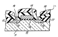
- The drawing shows in section a semiconductive device, for example, a
conventional MOS transistor 10, which comprises asubstrate 11, typically monocrystalline silicon which includes spaced source anddrain regions 12 and 13, respectively, to each of which a separate low resistance connection needs to be made. Additionally, the transistor includes agate 15 which overlies the channel region between the source and drain and is insulated therefrom by athin oxide film 16. Thickfield oxide regions 17 are used to isolate the transistor from other portions of the integrated circuit. It is generally necessary to provide an insulating film orlayer 18 which extends over the transistor to isolate the substrate and gate from overlying metal layers (not shown) which provide connections to the source drain and gate and interconnections between the circuit elements. Typically, thislayer 18 is of a dielectric material such as silicon oxide. Since low resistance connection needs to be made to the source and drain regions, theseportions 19 of thelayer 18 shown stippled in the drawing, overlying the source and drain either to be opened up or converted to a good conductor. This has proved a difficult problem particularly when the source and drain are relatively shallow and of limited surface area. - In accordance with the invention, the
layer 18 is made of a semiconductive material which has a relatively wide band gap to be of high resistivity in its intrinsic or undoped state but which can be implanted with dopants to have its resistivity sufficiently reduced in the implanted region that such region acts as a conductor, permitting a low resistance connection therethrough to the source and drain. - To this end, there is first deposited a
uniform layer 18 of the chosen material, carbon, over the transistor, to a sufficient thickness that it can serve as a satisfactory dielectric layer for isolating the substrate from the overlying metal layers to be deposited over thelayer 18. This requires a thickness adequate to avoid pinholes and typically will be 500 nm (5000 Angstroms) thick. The carbon layer is then coated with a layer of aphotoresist 20 of the kind normally used for photolithographic patterning. The photoresist is then patterned in the usual fashion to form openings in the photoresist selectively over the stippled regions oflayer 18 to be converted to low resistivity by implantation. After the openings are formed, thelayer 18 is implanted with dopants of the type to convert the implanted regions to the same conductivity type as the source and drain. Typically, these are N-type for the popular N-channel transistor in which case nitrogen can be implanted to make the implanted carbon N-type. After implantation, and stripping of the remaining photoresist, the transistor is annealed in the usual fashion to activate the implanted ions by substituting them in the carbon lattice. Annealing at about 900 C is typical. A typical doping would be average concentration of about nitrogen 10exp17 -10exp18 ions per CC. - Any of known techniques can be used for depositing the carbon. Typically, these involve a radio frequency plasma deposition process using a hydrocarbon gas as the carbon source. Other known processes involve ion beams, ion plating or pulsed plasmas.
- In some instances, it may prove advantageous first to thin the carbon film selectively where its resistivity is to be reduced to reduce the accelerating voltage which needs to be used to implant the nitrogen ions the full thickness of the film. This can readily be done by coating the film with a positive photoresist, developing the photoresist appropriately, and etching the photoresist in an oxygen plasma such that where the photoresist is removed first and the carbon film exposed, continued etching will thin the carbon film. After thinning the carbon film, the process proceeds as before.
- The choice of carbon is advantageous for several reasons. It is easily deposited and generally is not entirely amorphous as deposited but is a form of substantially crystalline phase intermediate between graphite and diamond with a definite band-gap which is wide and so made for good insulating properties with little temperature sensitivity. Additionally, carbon has good interface properties with silicon and silicon oxide. Finally, its susceptibility to etching in an oxygen plasma allows etching back planarization by use of a sacrificial photoresist.
Claims (2)
- A process of manufacturing an integrated circuit in which a low resistance connection (19) is to be made to a localized region (12; 13) of a semiconductive substrate (10) of one conductivity type underlying a layer which is normally an insulating layer (18) characterised by forming the normally insulating layer of a wide band-gap undoped semiconductive carbon to be of high resistivity, and implanting selectively the portion (19) of the layer (18) overlying the region to be connected with a dopant of the same conductivity type as the localized region.
- A process according to claim 1 in which the dopant implanted is nitrogen to make the implanted portion n-type.
Applications Claiming Priority (2)
| Application Number | Priority Date | Filing Date | Title |
|---|---|---|---|
| US920251 | 1986-10-17 | ||
| US06/920,251 US4722913A (en) | 1986-10-17 | 1986-10-17 | Doped semiconductor vias to contacts |
Publications (2)
| Publication Number | Publication Date |
|---|---|
| EP0265331A1 EP0265331A1 (en) | 1988-04-27 |
| EP0265331B1 true EP0265331B1 (en) | 1992-08-05 |
Family
ID=25443438
Family Applications (1)
| Application Number | Title | Priority Date | Filing Date |
|---|---|---|---|
| EP87402316A Expired - Lifetime EP0265331B1 (en) | 1986-10-17 | 1987-10-16 | Doped semiconductor vias to contacts |
Country Status (5)
| Country | Link |
|---|---|
| US (1) | US4722913A (en) |
| EP (1) | EP0265331B1 (en) |
| JP (1) | JPS63120442A (en) |
| KR (1) | KR960004589B1 (en) |
| DE (1) | DE3780907T2 (en) |
Families Citing this family (15)
| Publication number | Priority date | Publication date | Assignee | Title |
|---|---|---|---|---|
| US4972250A (en) * | 1987-03-02 | 1990-11-20 | Microwave Technology, Inc. | Protective coating useful as passivation layer for semiconductor devices |
| US4843034A (en) * | 1987-06-12 | 1989-06-27 | Massachusetts Institute Of Technology | Fabrication of interlayer conductive paths in integrated circuits |
| JPH07114237B2 (en) * | 1987-08-26 | 1995-12-06 | 株式会社東芝 | Semiconductor device |
| JP2546696B2 (en) * | 1987-12-17 | 1996-10-23 | 富士通株式会社 | Silicon carbide layer structure |
| EP0327336B1 (en) * | 1988-02-01 | 1997-12-10 | Semiconductor Energy Laboratory Co., Ltd. | Electronic devices incorporating carbon films |
| US5272361A (en) * | 1989-06-30 | 1993-12-21 | Semiconductor Energy Laboratory Co., Ltd. | Field effect semiconductor device with immunity to hot carrier effects |
| JPH03192754A (en) * | 1989-12-22 | 1991-08-22 | Omron Corp | Semiconductor device and manufacture thereof |
| JPH05343350A (en) * | 1992-06-08 | 1993-12-24 | Mitsubishi Electric Corp | Semiconductor device and manufacture thereof |
| US5514902A (en) | 1993-09-16 | 1996-05-07 | Mitsubishi Denki Kabushiki Kaisha | Semiconductor device having MOS transistor |
| US6927826B2 (en) * | 1997-03-26 | 2005-08-09 | Semiconductor Energy Labaratory Co., Ltd. | Display device |
| JPH10268360A (en) | 1997-03-26 | 1998-10-09 | Semiconductor Energy Lab Co Ltd | Display device |
| US6350672B1 (en) * | 1997-07-28 | 2002-02-26 | United Microelectronics Corp. | Interconnect structure with gas dielectric compatible with unlanded vias |
| JPH11307782A (en) | 1998-04-24 | 1999-11-05 | Semiconductor Energy Lab Co Ltd | Semiconductor device and its manufacture |
| US6713234B2 (en) * | 1999-02-18 | 2004-03-30 | Micron Technology, Inc. | Fabrication of semiconductor devices using anti-reflective coatings |
| US6475836B1 (en) * | 1999-03-29 | 2002-11-05 | Semiconductor Energy Laboratory Co., Ltd. | Semiconductor device and manufacturing method thereof |
Citations (3)
| Publication number | Priority date | Publication date | Assignee | Title |
|---|---|---|---|---|
| US4214918A (en) * | 1978-10-12 | 1980-07-29 | Stanford University | Method of forming polycrystalline semiconductor interconnections, resistors and contacts by applying radiation beam |
| US4472210A (en) * | 1983-01-07 | 1984-09-18 | Rca Corporation | Method of making a semiconductor device to improve conductivity of amorphous silicon films |
| US4511445A (en) * | 1982-06-18 | 1985-04-16 | At&T Bell Laboratories | Process of enhancing conductivity of material |
Family Cites Families (2)
| Publication number | Priority date | Publication date | Assignee | Title |
|---|---|---|---|---|
| US3922708A (en) * | 1974-03-04 | 1975-11-25 | Ibm | Method of producing high value ion implanted resistors |
| US4392298A (en) * | 1981-07-27 | 1983-07-12 | Bell Telephone Laboratories, Incorporated | Integrated circuit device connection process |
-
1986
- 1986-10-17 US US06/920,251 patent/US4722913A/en not_active Expired - Lifetime
-
1987
- 1987-10-16 JP JP62261530A patent/JPS63120442A/en active Pending
- 1987-10-16 DE DE8787402316T patent/DE3780907T2/en not_active Expired - Fee Related
- 1987-10-16 KR KR1019870011470A patent/KR960004589B1/en not_active IP Right Cessation
- 1987-10-16 EP EP87402316A patent/EP0265331B1/en not_active Expired - Lifetime
Patent Citations (3)
| Publication number | Priority date | Publication date | Assignee | Title |
|---|---|---|---|---|
| US4214918A (en) * | 1978-10-12 | 1980-07-29 | Stanford University | Method of forming polycrystalline semiconductor interconnections, resistors and contacts by applying radiation beam |
| US4511445A (en) * | 1982-06-18 | 1985-04-16 | At&T Bell Laboratories | Process of enhancing conductivity of material |
| US4472210A (en) * | 1983-01-07 | 1984-09-18 | Rca Corporation | Method of making a semiconductor device to improve conductivity of amorphous silicon films |
Also Published As
| Publication number | Publication date |
|---|---|
| KR880005662A (en) | 1988-06-29 |
| KR960004589B1 (en) | 1996-04-09 |
| EP0265331A1 (en) | 1988-04-27 |
| JPS63120442A (en) | 1988-05-24 |
| US4722913A (en) | 1988-02-02 |
| DE3780907T2 (en) | 1992-12-24 |
| DE3780907D1 (en) | 1992-09-10 |
Similar Documents
| Publication | Publication Date | Title |
|---|---|---|
| US4149307A (en) | Process for fabricating insulated-gate field-effect transistors with self-aligned contacts | |
| EP0043943B1 (en) | Method for forming field effect transistor integrated circuits having a pattern of narrow dimensioned dielectric regions and resulting structures | |
| US4422885A (en) | Polysilicon-doped-first CMOS process | |
| EP0110211B1 (en) | Bipolar transistor integrated circuit and method for manufacturing | |
| US4319395A (en) | Method of making self-aligned device | |
| EP0265331B1 (en) | Doped semiconductor vias to contacts | |
| US4317686A (en) | Method of manufacturing field-effect transistors by forming double insulative buried layers by ion-implantation | |
| US4735917A (en) | Silicon-on-sapphire integrated circuits | |
| EP0043944A2 (en) | Method for making a self-aligned field effect transistor integrated circuit structure | |
| US4735913A (en) | Self-aligned fabrication process for GaAs MESFET devices | |
| US4488162A (en) | Self-aligned metal field effect transistor integrated circuits using polycrystalline silicon gate electrodes | |
| WO1986007491A1 (en) | Process for forming contacts and interconnects for integrated circuits | |
| US4322883A (en) | Self-aligned metal process for integrated injection logic integrated circuits | |
| US4471522A (en) | Self-aligned metal process for field effect transistor integrated circuits using polycrystalline silicon gate electrodes | |
| EP0442296B1 (en) | A high speed silicon-on-insulator device and process of fabricating same | |
| US4520553A (en) | Process for manufacturing an integrated insulated-gate field-effect transistor | |
| US4513303A (en) | Self-aligned metal field effect transistor integrated circuit | |
| EP0073075B1 (en) | Semiconductor device comprising polycrystalline silicon and method of producing the same | |
| JPH0758343A (en) | Manufacture of mis transistor | |
| US5175127A (en) | Self-aligned interlayer contact process using a plasma etch of photoresist | |
| US4658495A (en) | Method of forming a semiconductor structure | |
| US5236852A (en) | Method for contacting a semiconductor device | |
| US5528053A (en) | Thin-film transistor and method for the manufacture thereof | |
| EP0066675B1 (en) | Processes for the fabrication of field effect transistors | |
| US5021358A (en) | Semiconductor fabrication process using sacrificial oxidation to reduce tunnel formation during tungsten deposition |
Legal Events
| Date | Code | Title | Description |
|---|---|---|---|
| PUAI | Public reference made under article 153(3) epc to a published international application that has entered the european phase |
Free format text: ORIGINAL CODE: 0009012 |
|
| AK | Designated contracting states |
Kind code of ref document: A1 Designated state(s): DE ES FR GB IT NL |
|
| 17P | Request for examination filed |
Effective date: 19880721 |
|
| 17Q | First examination report despatched |
Effective date: 19910327 |
|
| PGFP | Annual fee paid to national office [announced via postgrant information from national office to epo] |
Ref country code: GR Payment date: 19910925 Year of fee payment: 5 |
|
| RAP1 | Party data changed (applicant data changed or rights of an application transferred) |
Owner name: SGS-THOMSON MICROELECTRONICS, INC. |
|
| GRAA | (expected) grant |
Free format text: ORIGINAL CODE: 0009210 |
|
| AK | Designated contracting states |
Kind code of ref document: B1 Designated state(s): DE ES FR GB IT NL |
|
| PG25 | Lapsed in a contracting state [announced via postgrant information from national office to epo] |
Ref country code: NL Effective date: 19920805 |
|
| ITF | It: translation for a ep patent filed |
Owner name: JACOBACCI CASETTA & PERANI S.P.A. |
|
| REF | Corresponds to: |
Ref document number: 3780907 Country of ref document: DE Date of ref document: 19920910 |
|
| ET | Fr: translation filed | ||
| PG25 | Lapsed in a contracting state [announced via postgrant information from national office to epo] |
Ref country code: ES Free format text: LAPSE BECAUSE OF FAILURE TO SUBMIT A TRANSLATION OF THE DESCRIPTION OR TO PAY THE FEE WITHIN THE PRESCRIBED TIME-LIMIT Effective date: 19921116 |
|
| NLV1 | Nl: lapsed or annulled due to failure to fulfill the requirements of art. 29p and 29m of the patents act | ||
| PLBE | No opposition filed within time limit |
Free format text: ORIGINAL CODE: 0009261 |
|
| STAA | Information on the status of an ep patent application or granted ep patent |
Free format text: STATUS: NO OPPOSITION FILED WITHIN TIME LIMIT |
|
| 26N | No opposition filed | ||
| REG | Reference to a national code |
Ref country code: GB Ref legal event code: 732E |
|
| REG | Reference to a national code |
Ref country code: FR Ref legal event code: TP |
|
| PGFP | Annual fee paid to national office [announced via postgrant information from national office to epo] |
Ref country code: GB Payment date: 19971007 Year of fee payment: 11 |
|
| PGFP | Annual fee paid to national office [announced via postgrant information from national office to epo] |
Ref country code: FR Payment date: 19971009 Year of fee payment: 11 |
|
| PGFP | Annual fee paid to national office [announced via postgrant information from national office to epo] |
Ref country code: DE Payment date: 19971024 Year of fee payment: 11 |
|
| PG25 | Lapsed in a contracting state [announced via postgrant information from national office to epo] |
Ref country code: GB Free format text: LAPSE BECAUSE OF NON-PAYMENT OF DUE FEES Effective date: 19981016 |
|
| GBPC | Gb: european patent ceased through non-payment of renewal fee |
Effective date: 19981016 |
|
| PG25 | Lapsed in a contracting state [announced via postgrant information from national office to epo] |
Ref country code: FR Free format text: LAPSE BECAUSE OF NON-PAYMENT OF DUE FEES Effective date: 19990630 |
|
| REG | Reference to a national code |
Ref country code: FR Ref legal event code: ST |
|
| PG25 | Lapsed in a contracting state [announced via postgrant information from national office to epo] |
Ref country code: DE Free format text: LAPSE BECAUSE OF NON-PAYMENT OF DUE FEES Effective date: 19990803 |
|
| PG25 | Lapsed in a contracting state [announced via postgrant information from national office to epo] |
Ref country code: IT Free format text: LAPSE BECAUSE OF NON-PAYMENT OF DUE FEES;WARNING: LAPSES OF ITALIAN PATENTS WITH EFFECTIVE DATE BEFORE 2007 MAY HAVE OCCURRED AT ANY TIME BEFORE 2007. THE CORRECT EFFECTIVE DATE MAY BE DIFFERENT FROM THE ONE RECORDED. Effective date: 20051016 |