EP0264726A2 - Picture transformation memory - Google Patents
Picture transformation memory Download PDFInfo
- Publication number
- EP0264726A2 EP0264726A2 EP87114684A EP87114684A EP0264726A2 EP 0264726 A2 EP0264726 A2 EP 0264726A2 EP 87114684 A EP87114684 A EP 87114684A EP 87114684 A EP87114684 A EP 87114684A EP 0264726 A2 EP0264726 A2 EP 0264726A2
- Authority
- EP
- European Patent Office
- Prior art keywords
- field
- pixel
- data
- planes
- picture
- Prior art date
- Legal status (The legal status is an assumption and is not a legal conclusion. Google has not performed a legal analysis and makes no representation as to the accuracy of the status listed.)
- Granted
Links
Images


Classifications
-
- G—PHYSICS
- G06—COMPUTING; CALCULATING OR COUNTING
- G06T—IMAGE DATA PROCESSING OR GENERATION, IN GENERAL
- G06T3/00—Geometric image transformation in the plane of the image
- G06T3/60—Rotation of a whole image or part thereof
- G06T3/606—Rotation by memory addressing or mapping
-
- G—PHYSICS
- G11—INFORMATION STORAGE
- G11C—STATIC STORES
- G11C7/00—Arrangements for writing information into, or reading information out from, a digital store
-
- H—ELECTRICITY
- H04—ELECTRIC COMMUNICATION TECHNIQUE
- H04N—PICTORIAL COMMUNICATION, e.g. TELEVISION
- H04N5/00—Details of television systems
- H04N5/222—Studio circuitry; Studio devices; Studio equipment
- H04N5/262—Studio circuits, e.g. for mixing, switching-over, change of character of image, other special effects ; Cameras specially adapted for the electronic generation of special effects
- H04N5/2628—Alteration of picture size, shape, position or orientation, e.g. zooming, rotation, rolling, perspective, translation
-
- H—ELECTRICITY
- H04—ELECTRIC COMMUNICATION TECHNIQUE
- H04N—PICTORIAL COMMUNICATION, e.g. TELEVISION
- H04N5/00—Details of television systems
- H04N5/76—Television signal recording
- H04N5/907—Television signal recording using static stores, e.g. storage tubes or semiconductor memories
Landscapes
- Engineering & Computer Science (AREA)
- Multimedia (AREA)
- Signal Processing (AREA)
- Physics & Mathematics (AREA)
- General Physics & Mathematics (AREA)
- Theoretical Computer Science (AREA)
- Studio Circuits (AREA)
- Image Input (AREA)
- Image Processing (AREA)
Abstract
Description
- The present invention relates to digital memory architectures, and more particular to a picture transformation memory for use with a digital video effects system.
- A digital video effects system receives video data, either analog or digital, from various sources, such as cameras, video tapes and discs, etc., via an input section. The video data is converted to a desired digital format in the input section and appropriately filtered according to the effects which are desired at the output of the system. The filtered digital video data is then transformed, i.e., a transform section performs spatial transformations, such as enlargement, reduction, translation and rotation. The digital video data, representing a picture image, is written into a frame buffer in a normal, unchanged way using a first set of addresses generated by an input address generator. An output address generator, sometimes called a reverse or transformation address generator, reads the picture image out of the frame buffer in such a manner as to create the desired transform. An address limit detector senses when a given output address is outside the frame buffer's address range and blanks the video for those addresses. The addresses from the transformation address generator are derived from the original addresses of an output display screen, such as a televison monitor, multiplied by a transform matrix Tʹ. Besides the video frame buffer to store the luminance and chrominance components of the picture, a key frame buffer is also operated in parallel to provide shape and transparency information about the picture, the key being transformed in a like manner as the picture. The transformed picture from the frame buffer is mixed with a background picture image in proportion to the key value (between 0 and 1) to produce the final picture image which is displayed.
- When transforming an interlaced video picture in a digital video effects system, it is desirable to perform the video processing on a full frame as if the picture image were not interlaced. Such a spatial transformation system is described in U.S. Patent No. 4,463,372 entitled "Spatial Transformation System Including Key Signal Generator" issued to Phillip P. Bennett and Steven A. Gabriel on July 31, 1984. At Fig. 6 and
column 19 of that patent a particular memory architecture is described which uses three full field buffer memories. The input to the three buffer memories is the digitized video picture image to be transformed or otherwise processed by the digital video effects system. The field buffers operate on a continuous revolving basis in that one buffer receives an incoming field of data while the other two buffers, containing the newest complete field of data and the prior complete field of data, provide outputs via a multiplexer which together make up a complete picture frame of data. Thus a field buffer memory on consecutive data fields first receives an input field of data, then outputs the newest complete field of data, and finally outputs the prior complete field of data, the cycle repeating itself every three fields. - Real time television frame stores require significant quantities of semiconductor memory. Since the picture elements (pixels) occur at approximately 70 nanosecond intervals, current practically available memory storage chips which are inexpensive and relatively low in power consumption cannont be accessed at pixel clock rates. To accommodate the required bandwidth the Bennett et al patent implements each field buffer memory as eight modules of 32Kx8 memory which are addressed sequentially, i.e., once every eight pixel clock periods. This method, however, requires that the stored data be accessed in a specific order and is not a totally random access frame store.
- As indicated there are three channels of data that are transformed in parallel: a luminance channel, a chrominance channel and an associated key channel. To facilitate manufacture and maintenance of the digital video effects system it is advantageous for the hardware in each channel to be interchangeable. However standard television formats provide a full bandwidth luminance component of video and two half bandwidth chrominance components of the video which requires different processing for the luminance and chrominance components. Further, when pictures are transformed, it is necessary to obtain pixels between actual pixels stored in the frame store to provide smooth movement and continuity of the picture. Therefore, interpolation is required, and such interpolation requires access not just to one pixel from the frame store, but to neighboring pixels as well. What is desired is a picture transformation memory which provides identical frame stores for both full bandwidth signals and half bandwidth signals to allow interchangeability of the various frame stores within a digital video effects system, which provides a fully random accessible output of an addressed pixel together with its neighbors to an interpolator, and which allows manipulation of a full frame of data at apparent real time pixel rates.
- Accordingly the present invention provides a picture transformation memory for a digital video effects system which has three field store memories, each field store having four planes and each plane having four banks. Digitized video data representing a picture image is input to the frame store on a field by field basis. As one field of the picture image is being written into one field store memory, the current field and the prior field are being read out of the other two field store memories to provide a complete frame of the picture image. Each plane of a field store memory contains the same field of picture video data for a full bandwidth component such as luminance and alternate planes contain the same field of picture video data for half bandwidth components such as chrominance video data, while each bank within the plane contains one-fourth of the field of picture video, the pixels of the picture video data being read sequentially into consecutive banks. For each pixel addressed for output four contiguous pixels, representing one field from one field store memory, or eight contiguous pixels, representing two fields from two of the field store memories, are output to an interpolator for processing. When a full bandwidth field store memory is accessed, the pixels are output at the pixel clock rate from consecutive planes of the memory. When a half bandwidth field store memory is accessed, the pixels are output at the pixel clock rate from consecutive planes of the memory, but the address is held the same for two clock cycles to access the two chrominance components. Thus it is the addressing rather than the hardware which differentiates between the full and half bandwidth channels.
- The objects, advantages and novel features of the present will be apparent from the following detailed description when read in conjunction with the appended claims and attached drawing.
-
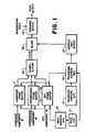
- Fig. 1 is a block diagram of a portion of a digital video effects system.
- Fig. 2 is a block diagram view of one of the frame stores of Fig. 1 according to the present invention.
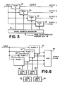
- Fig. 3 is a block diagram view of one of the field stores making up the frame store of Fig. 2.
- Fig. 4 is a graphical illustration of the addressing of the field store of Fig. 3.
- Fig. 5 is a graphical illustration of the addressing of two field stores representing a complete frame.
- Fig. 6 is a block diagram view of one of the banks making up the field store of Fig. 3.
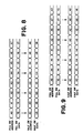
- Fig. 7 is a graphical illustation of the storage of half bandwidth data in respective planes of the field store of Fig. 3.
- Fig. 8 is a graphical illustration of the output of full bandwidth and half bandwidth data from the planes of Fig. 6 for consecutive pixels.
- Fig. 9 is a graphical illustration of the output of full bandwidth and half bandwidth data from the planes of Fig. 6 for non-consecutive pixels.
- Referring now to Fig. 1 a portion of a digital video effects system incorporating the picture transformation memory of the present invention is shown. Video components of a picture image, such as a full bandwidth luminance component and two half bandwidth chrominance components according to a standard television digital format, are written into respective luminance and
chrominance frame buffers address generator 15 which is clocked by apixel clock 17. A corresponding full bandwidth key component is also written into akey frame buffer 25 under control of the write address generator. The picture image is read out of therespective frame buffers transforamtion address generator 19 which is also clocked by thepixel clock 17. The sequence of addresses from thetransformation address generator 19 is the product of sequential display addresses and a transform function Tʹ determined by operator input via aninterface controller 21. The output from theframe buffers interpolator 23 to produce an intermediate pixel for smooth motion of the transformed picture. The address from thetransformation address generator 19 is checked by anaddress limit detector 27 which inhibits via ablanking circuit 29 video outputs for invalid frame buffer addresses. The components are combined, or further processed, by acombiner circuit 33 and mixed with a background video signal according to the key signal, the key signal having undergone the same transformation as the picture image. The output of thecombiner circuit 33 is the desired, transformed picture image for display. - Fig. 2 shows one of the
frame stores field store memories selector 18. Digitized video data, either full bandwidth luminance data or half bandwidth chrominance data depending upon theframe field store memories crosspoint switching circuit 20 and thewrite address generator 15. As selected by read signals from thecrosspoint switching circuit 20 theoutput address generators field store memories selector 18 as determined by the addresses from thetransformation address generator 19. A select signal CTL1 is applied to the 3:2selector 18 to determine which of the three field stores contains current complete field data, which contains prior complete field data, and which is to be ignored for output. The output of the 3:2selector 18 it two fields of data making up a full picture frame including the current complete field of data and the prior complete field of data. - For example at field time N field store one 12 is selected to receive the next field of digitized video from the input line, field store two 14 is selected to provide the prior complete field of data to the 3:2
selector 18, and field store three 16 is selected to provide the current complete field of data to the selector. At field time N+1 field store one now contains the current complete field of data for output to theselector 18, field store two is receiving a new field of data from the input line, and field store three contains the prior complete field of data for output to the selector. At field time N+2 field store one contains the prior complete field of data for output to the selector, field store two contains the current complete field of data for output to the selector, and field store three is receiving a new field of data from the input line. At time N+4 the cycle is started over again with field store one receiving a new field of data from the input line. In this way the output ofselector 18 provides the most recent complete frame of data for further processing by the digital video effects system. - Each
field store memory banks transformation address generator 19 points at the upper left corner of a desired set of four pixels to be accessed. Alocal address generator 36 determines what address to access in each of the fourbanks local address generator 36 are calculated as follows:
Upper left pixel = n
Upper right pixel = n + 1 column
Lower left pixel = n + 1 row
Lower right pixel = n + 1 row + 1 column
It can be seen from Fig. 4 that the two least significant bits of the row address signal, which are labeled Y0 and Y1, and the least significant bit of the column address signal, which is labeled X0, from the picture transformation address generator can be used to determine the bank orientation of the desired pixel quad. - Fig. 5 shows this concept extended to a complete two field frame by using two field stores, each organized into four banks as described above and using the three least significant bits of RAS. The
local address generator 36 translates the frame addresses from the picture transformation address generator into field addresses as follows:
Field 1 Address = (Frame Address)/2
Field 2 Address = (Frame Address + 1)/2
These addresses are used as described above to provide eight simultaneous pixels, two horizontally and four vertically, which an interpolator can use to perform a higher order vertical interpolation if required. Such an interpolator is described in co-pending U.S. Patent Application No. entitled "Adaptive Two Dimensional Interpolator" by John Abt and Richard A. Jackson, filed . - Besides being composed of four
banks field store identical planes plane own address generator output multiplexer 54 selects one of the four memory planes in sequence to provide the output. - When data is written into each
field store field store first plane 38 is accessing the first pixel together with the neighboring pixels as described above, the second pixel is being requested from plane two 40. Likewise while the first andsecond planes - The
output multiplexer 54 is synchronized with the data available at the output from eachplane multiplexer 54 is a continuous stream of pixels transparent to the fact that each came from a different memory plane. This independently addressable scheme provides for a totally random access of pixels. For example the upper left pixel of a stored picture may be followed by the lower right pixel followed in turn by the center pixel or any other combination desired. - When writing data into the field stores 12, 14, 16 in the full bandwidth mode, all four
planes - When the picture is read from the field store, the first pixel requested is accessed from plane one 38 having U data. The address is then held while the correspoding V pixel is accessed from the same address of plane two 40. Similarly the second pixel of U data is accessed from plane three 42 and the corresponding V pixel is accessed from plane four 44. As with the full bandwidth case, the access upon reading from the field store is totally random. If the first pixel is read from address 1 (full bandwidth), the half bandwidth memory ignores the least significant bit and accesses U data from
address 0 in plane one 38 followed on the next clock cycle byaddress 0 in plane two 40 for the corresponding V pixel. Fig. 8 illustrates this reading process for an untransformed picture, i.e., the same picture is output as was input, while Fig. 9 illustrates the reading process for a transformed picture randomly accessed. - Thus the present invention provides a totally randomly accessible picture transformation memory which provides smooth picture continuity and identical hardware for both full and half bandwidth video picture components by using a three field frame store with each field having four banks and each bank having four planes, the output of the banks providing an addressed and neighboring pixels for input to an interpolator and the addressing of the planes determiing whether full or half bandwidth data is being read.
Claims (6)
a plurality of banks making up each field store, the banks for each field store having the total capacity to store one complete field of input digitized video data; and
means for accessing the video data stored in the plurality of banks such that, when a given pixel of the video data is requested for access, neighboring pixels from each bank are automatically accessed to produce a multi-pixel output for input to an interpolator.
a plurality of planes, each plane having the capacity to store a full field of the digitized video data representing a picture and being divided into the plurality of banks such that each plane contains the identical picture;
means for addressing each plane independently of the other planes depending upon a desired transformation of the picuture; and
means for multiplexing the outputs of the planes sequentially to produce an output field of video data which is transparent of the fact that each pixel that makes up the output field comes from a different one of the planes.
means for randomly accessing any pixel of full bandwidth data contained in one of the field stores; and
means for accessing the corresponding half bandwidth data components by ignoring the least significant bit of an address word produced by the randomly accessing means for the full bandwidth data and using the truncated address word for accessing consecutive planes.
Applications Claiming Priority (2)
| Application Number | Priority Date | Filing Date | Title |
|---|---|---|---|
| US06/920,560 US4743970A (en) | 1986-10-20 | 1986-10-20 | Picture transformation memory |
| US920560 | 1986-10-20 |
Publications (3)
| Publication Number | Publication Date |
|---|---|
| EP0264726A2 true EP0264726A2 (en) | 1988-04-27 |
| EP0264726A3 EP0264726A3 (en) | 1990-11-07 |
| EP0264726B1 EP0264726B1 (en) | 1994-05-04 |
Family
ID=25443957
Family Applications (1)
| Application Number | Title | Priority Date | Filing Date |
|---|---|---|---|
| EP87114684A Expired - Lifetime EP0264726B1 (en) | 1986-10-20 | 1987-10-08 | Picture transformation memory |
Country Status (6)
| Country | Link |
|---|---|
| US (1) | US4743970A (en) |
| EP (1) | EP0264726B1 (en) |
| JP (1) | JP2558236B2 (en) |
| AU (1) | AU591350B2 (en) |
| CA (1) | CA1252877A (en) |
| DE (1) | DE3789750T2 (en) |
Cited By (7)
| Publication number | Priority date | Publication date | Assignee | Title |
|---|---|---|---|---|
| EP0291347A2 (en) * | 1987-05-15 | 1988-11-17 | Pioneer Electronic Corporation | Image processing method and apparatus |
| WO1990007842A2 (en) * | 1988-12-23 | 1990-07-12 | Rank Cintel Limited | Compensation of losses and defects in telecine devices |
| EP0449210A2 (en) * | 1990-03-30 | 1991-10-02 | Kabushiki Kaisha Toshiba | Electronic zooming device |
| EP0462396A2 (en) * | 1990-06-20 | 1991-12-27 | International Business Machines Corporation | Triple field buffer for television image storage and visualization on raster graphics display |
| EP0506429A2 (en) * | 1991-03-29 | 1992-09-30 | The Grass Valley Group, Inc. | Video image mapping system |
| EP0529866A2 (en) * | 1991-08-22 | 1993-03-03 | International Business Machines Corporation | Processor for a multiprocessor system |
| EP0662772A2 (en) * | 1994-01-07 | 1995-07-12 | Matsushita Electric Industrial Co., Ltd. | Segmentation based image compression system |
Families Citing this family (19)
| Publication number | Priority date | Publication date | Assignee | Title |
|---|---|---|---|---|
| GB8622613D0 (en) * | 1986-09-19 | 1986-10-22 | Questech Ltd | Processing of video image signals |
| GB8622610D0 (en) * | 1986-09-19 | 1986-10-22 | Questech Ltd | Processing of video image signals |
| US5005126A (en) * | 1987-04-09 | 1991-04-02 | Prevail, Inc. | System and method for remote presentation of diagnostic image information |
| JP2687397B2 (en) * | 1988-02-29 | 1997-12-08 | 松下電器産業株式会社 | Image memory and image processing device |
| US4872054A (en) * | 1988-06-30 | 1989-10-03 | Adaptive Video, Inc. | Video interface for capturing an incoming video signal and reformatting the video signal |
| US4920415A (en) * | 1989-03-20 | 1990-04-24 | The Grass Valley Group, Inc. | Self keyer |
| JP2771858B2 (en) * | 1989-08-23 | 1998-07-02 | 富士通株式会社 | Multi-screen synthesis device |
| GB9012326D0 (en) * | 1990-06-01 | 1990-07-18 | Thomson Consumer Electronics | Wide screen television |
| US5311309A (en) * | 1990-06-01 | 1994-05-10 | Thomson Consumer Electronics, Inc. | Luminance processing system for compressing and expanding video data |
| US5321798A (en) * | 1991-10-28 | 1994-06-14 | Hughes Aircraft Company | Apparatus for providing a composite digital representation of a scene within a field-of-regard |
| EP0616466B1 (en) * | 1992-01-07 | 2000-06-07 | Thomson Consumer Electronics, Inc. | Horizontal panning for wide screen television |
| US5287188A (en) * | 1992-01-07 | 1994-02-15 | Thomson Consumer Electronics, Inc. | Horizontal panning for wide screen television |
| GB9200281D0 (en) * | 1992-01-08 | 1992-02-26 | Thomson Consumer Electronics | A pip horizontal panning circuit for wide screen television |
| US5274472A (en) * | 1992-05-21 | 1993-12-28 | Xerox Corporation | High addressability image generator using pseudo interpolation of video and screen data |
| US5905538A (en) * | 1997-10-15 | 1999-05-18 | Tektronix, Inc. | System of switching video of two different standards |
| US6205181B1 (en) * | 1998-03-10 | 2001-03-20 | Chips & Technologies, Llc | Interleaved strip data storage system for video processing |
| JP2004516718A (en) * | 2000-12-11 | 2004-06-03 | コーニンクレッカ フィリップス エレクトロニクス エヌ ヴィ | Motion compensated deinterlacing in video signal processing |
| US6760035B2 (en) * | 2001-11-19 | 2004-07-06 | Nvidia Corporation | Back-end image transformation |
| KR100695141B1 (en) * | 2005-02-15 | 2007-03-14 | 삼성전자주식회사 | Memory access apparatus and method, data write/read apparatus and method for use in image processing system |
Citations (4)
| Publication number | Priority date | Publication date | Assignee | Title |
|---|---|---|---|---|
| US4463372A (en) * | 1982-03-24 | 1984-07-31 | Ampex Corporation | Spatial transformation system including key signal generator |
| GB2158322A (en) * | 1984-04-25 | 1985-11-06 | Quantel Ltd | Improvements in or relating to video signal processing systems |
| EP0174700A1 (en) * | 1984-09-14 | 1986-03-19 | Philips Electronics Uk Limited | Apparatus for processing video signals |
| EP0176290A1 (en) * | 1984-09-25 | 1986-04-02 | Sony Corporation | Video signal memories |
Family Cites Families (9)
| Publication number | Priority date | Publication date | Assignee | Title |
|---|---|---|---|---|
| US4573070A (en) * | 1977-01-31 | 1986-02-25 | Cooper J Carl | Noise reduction system for video signals |
| US4322750A (en) * | 1979-05-08 | 1982-03-30 | British Broadcasting Corporation | Television display system |
| US4468747A (en) * | 1980-11-03 | 1984-08-28 | Hewlett-Packard Company | Scan converter system |
| US4432009A (en) * | 1981-03-24 | 1984-02-14 | Rca Corporation | Video pre-filtering in phantom raster generating apparatus |
| US4449143A (en) * | 1981-10-26 | 1984-05-15 | Rca Corporation | Transcodeable vertically scanned high-definition television system |
| GB2140644B (en) * | 1983-05-17 | 1986-09-17 | Sony Corp | Television standards converters |
| JPS60160780A (en) * | 1984-01-31 | 1985-08-22 | Nec Corp | Picture storage device for special effect |
| JPS6162286A (en) * | 1984-09-04 | 1986-03-31 | Univ Nagoya | Picture signal band compressing system |
| US4639769A (en) * | 1985-04-01 | 1987-01-27 | Eastman Kodak Company | Modifying color digital images |
-
1986
- 1986-10-20 US US06/920,560 patent/US4743970A/en not_active Expired - Fee Related
-
1987
- 1987-10-06 CA CA000548691A patent/CA1252877A/en not_active Expired
- 1987-10-08 DE DE3789750T patent/DE3789750T2/en not_active Expired - Fee Related
- 1987-10-08 EP EP87114684A patent/EP0264726B1/en not_active Expired - Lifetime
- 1987-10-19 AU AU79895/87A patent/AU591350B2/en not_active Ceased
- 1987-10-20 JP JP62265159A patent/JP2558236B2/en not_active Expired - Lifetime
Patent Citations (4)
| Publication number | Priority date | Publication date | Assignee | Title |
|---|---|---|---|---|
| US4463372A (en) * | 1982-03-24 | 1984-07-31 | Ampex Corporation | Spatial transformation system including key signal generator |
| GB2158322A (en) * | 1984-04-25 | 1985-11-06 | Quantel Ltd | Improvements in or relating to video signal processing systems |
| EP0174700A1 (en) * | 1984-09-14 | 1986-03-19 | Philips Electronics Uk Limited | Apparatus for processing video signals |
| EP0176290A1 (en) * | 1984-09-25 | 1986-04-02 | Sony Corporation | Video signal memories |
Cited By (17)
| Publication number | Priority date | Publication date | Assignee | Title |
|---|---|---|---|---|
| EP0291347B1 (en) * | 1987-05-15 | 1994-01-05 | Pioneer Electronic Corporation | Image processing method and apparatus |
| EP0291347A2 (en) * | 1987-05-15 | 1988-11-17 | Pioneer Electronic Corporation | Image processing method and apparatus |
| WO1990007842A2 (en) * | 1988-12-23 | 1990-07-12 | Rank Cintel Limited | Compensation of losses and defects in telecine devices |
| WO1990007842A3 (en) * | 1988-12-23 | 1990-09-07 | Rank Cintel Ltd | Compensation of losses and defects in telecine devices |
| US5327247A (en) * | 1988-12-23 | 1994-07-05 | Rank Cintel Ltd. | Compensation of losses and defects in telecine devices |
| US5351082A (en) * | 1990-03-30 | 1994-09-27 | Kabushiki Kaisha Toshiba | Signal-converting device |
| EP0449210A3 (en) * | 1990-03-30 | 1993-05-19 | Kabushiki Kaisha Toshiba | Electronic zooming device |
| EP0449210A2 (en) * | 1990-03-30 | 1991-10-02 | Kabushiki Kaisha Toshiba | Electronic zooming device |
| EP0462396A3 (en) * | 1990-06-20 | 1992-08-19 | International Business Machines Corporation | Triple field buffer for television image storage and visualization on raster graphics display |
| US5291275A (en) * | 1990-06-20 | 1994-03-01 | International Business Machines Incorporated | Triple field buffer for television image storage and visualization on raster graphics display |
| EP0462396A2 (en) * | 1990-06-20 | 1991-12-27 | International Business Machines Corporation | Triple field buffer for television image storage and visualization on raster graphics display |
| EP0506429A2 (en) * | 1991-03-29 | 1992-09-30 | The Grass Valley Group, Inc. | Video image mapping system |
| EP0506429A3 (en) * | 1991-03-29 | 1995-02-08 | Grass Valley Group | |
| EP0529866A2 (en) * | 1991-08-22 | 1993-03-03 | International Business Machines Corporation | Processor for a multiprocessor system |
| EP0529866A3 (en) * | 1991-08-22 | 1994-12-07 | Ibm | Processor for a multiprocessor system |
| EP0662772A2 (en) * | 1994-01-07 | 1995-07-12 | Matsushita Electric Industrial Co., Ltd. | Segmentation based image compression system |
| EP0662772A3 (en) * | 1994-01-07 | 1998-02-04 | Matsushita Electric Industrial Co., Ltd. | Segmentation based image compression system |
Also Published As
| Publication number | Publication date |
|---|---|
| US4743970A (en) | 1988-05-10 |
| EP0264726B1 (en) | 1994-05-04 |
| CA1252877A (en) | 1989-04-18 |
| DE3789750T2 (en) | 1994-11-03 |
| JPS63109670A (en) | 1988-05-14 |
| JP2558236B2 (en) | 1996-11-27 |
| DE3789750D1 (en) | 1994-06-09 |
| EP0264726A3 (en) | 1990-11-07 |
| AU591350B2 (en) | 1989-11-30 |
| AU7989587A (en) | 1988-04-21 |
Similar Documents
| Publication | Publication Date | Title |
|---|---|---|
| US4743970A (en) | Picture transformation memory | |
| US5124692A (en) | Method and apparatus for providing rotation of digital image data | |
| US5021772A (en) | Interactive real-time video processor with zoom pan and scroll capability | |
| US5227863A (en) | Programmable digital video processing system | |
| US5742349A (en) | Memory efficient video graphics subsystem with vertical filtering and scan rate conversion | |
| JP2656737B2 (en) | Data processing device for processing video information | |
| US4148070A (en) | Video processing system | |
| US5444483A (en) | Digital electronic camera apparatus for recording still video images and motion video images | |
| US5805148A (en) | Multistandard video and graphics, high definition display system and method | |
| US4878117A (en) | Video signal mixing unit for simultaneously displaying video signals having different picture aspect ratios and resolutions | |
| JPH04233592A (en) | Method and apparatus for displaying television image | |
| JPH0681304B2 (en) | Method converter | |
| US4811099A (en) | Video signal memories | |
| US4941127A (en) | Method for operating semiconductor memory system in the storage and readout of video signal data | |
| US4754279A (en) | Scan converter for radar | |
| US4647971A (en) | Moving video special effects system | |
| US5253062A (en) | Image displaying apparatus for reading and writing graphic data at substantially the same time | |
| JPS59205881A (en) | Electronic still memory system | |
| US6178289B1 (en) | Video data shuffling method and apparatus | |
| JPH07240891A (en) | Digital memory for display device using space light modulator | |
| GB2086690A (en) | Video image processing system | |
| JP2933937B2 (en) | A display processor for image data with pixel sizes that are not constant with respect to chromaticity values | |
| US4766496A (en) | Video signal memories | |
| JP2918049B2 (en) | Storage method for picture-in-picture | |
| JP3303979B2 (en) | Image playback device |
Legal Events
| Date | Code | Title | Description |
|---|---|---|---|
| PUAI | Public reference made under article 153(3) epc to a published international application that has entered the european phase |
Free format text: ORIGINAL CODE: 0009012 |
|
| AK | Designated contracting states |
Kind code of ref document: A2 Designated state(s): DE FR GB |
|
| PUAL | Search report despatched |
Free format text: ORIGINAL CODE: 0009013 |
|
| AK | Designated contracting states |
Kind code of ref document: A3 Designated state(s): DE FR GB |
|
| 17P | Request for examination filed |
Effective date: 19901102 |
|
| 17Q | First examination report despatched |
Effective date: 19920710 |
|
| GRAA | (expected) grant |
Free format text: ORIGINAL CODE: 0009210 |
|
| AK | Designated contracting states |
Kind code of ref document: B1 Designated state(s): DE FR GB |
|
| REF | Corresponds to: |
Ref document number: 3789750 Country of ref document: DE Date of ref document: 19940609 |
|
| ET | Fr: translation filed | ||
| PGFP | Annual fee paid to national office [announced via postgrant information from national office to epo] |
Ref country code: FR Payment date: 19940912 Year of fee payment: 8 |
|
| PLBE | No opposition filed within time limit |
Free format text: ORIGINAL CODE: 0009261 |
|
| STAA | Information on the status of an ep patent application or granted ep patent |
Free format text: STATUS: NO OPPOSITION FILED WITHIN TIME LIMIT |
|
| 26N | No opposition filed | ||
| PG25 | Lapsed in a contracting state [announced via postgrant information from national office to epo] |
Ref country code: FR Effective date: 19960628 |
|
| REG | Reference to a national code |
Ref country code: FR Ref legal event code: ST |
|
| PGFP | Annual fee paid to national office [announced via postgrant information from national office to epo] |
Ref country code: GB Payment date: 19990920 Year of fee payment: 13 |
|
| PGFP | Annual fee paid to national office [announced via postgrant information from national office to epo] |
Ref country code: DE Payment date: 19990930 Year of fee payment: 13 |
|
| PG25 | Lapsed in a contracting state [announced via postgrant information from national office to epo] |
Ref country code: GB Free format text: LAPSE BECAUSE OF NON-PAYMENT OF DUE FEES Effective date: 20001008 |
|
| GBPC | Gb: european patent ceased through non-payment of renewal fee |
Effective date: 20001008 |
|
| PG25 | Lapsed in a contracting state [announced via postgrant information from national office to epo] |
Ref country code: DE Free format text: LAPSE BECAUSE OF NON-PAYMENT OF DUE FEES Effective date: 20010703 |