EP0260887A2 - Colourburst regeneration - Google Patents
Colourburst regeneration Download PDFInfo
- Publication number
- EP0260887A2 EP0260887A2 EP87308046A EP87308046A EP0260887A2 EP 0260887 A2 EP0260887 A2 EP 0260887A2 EP 87308046 A EP87308046 A EP 87308046A EP 87308046 A EP87308046 A EP 87308046A EP 0260887 A2 EP0260887 A2 EP 0260887A2
- Authority
- EP
- European Patent Office
- Prior art keywords
- signal
- color burst
- phase
- information
- standard
- Prior art date
- Legal status (The legal status is an assumption and is not a legal conclusion. Google has not performed a legal analysis and makes no representation as to the accuracy of the status listed.)
- Granted
Links
Images

Classifications
-
- H—ELECTRICITY
- H04—ELECTRIC COMMUNICATION TECHNIQUE
- H04N—PICTORIAL COMMUNICATION, e.g. TELEVISION
- H04N9/00—Details of colour television systems
- H04N9/44—Colour synchronisation
- H04N9/455—Generation of colour burst signals; Insertion of colour burst signals in colour picture signals or separation of colour burst signals from colour picture signals
Definitions
- the present invention generally pertains to television signal processing and is particularly directed to regeneration of a color burst signal.
- an original standard-format video signal as shown in Figure 1A, containing a sinusoidal color burst signal 10 preceding the video information 12 in each horizontal line is converted into a format, such as shown in Figure 1B, wherein a color burst information signal 14 of less than standard length, but phase coincident with the color burst signal 10 in the original video signal ( Figure 1A) is positioned between segments of audio and/or control information 16 and video information 18.
- the less-than-standard length color burst information signal 14 in the converted signal is formed by truncating the color burst signal 10 in the original video signal and thus has the same frequency and phase as the standard-length color burst signal in the original video signal.
- the present invention provides a system for regenerating a standard- length color burst signal from a less-than-standard-length color burst information signal of a given frequency and phase.
- the system of the present invention includes means for generating a system clock signal from the color burst information signal, with the clock signal having a clock frequency related to and at least twice the given frequency of the color burst information signal; means for sampling and storing phase information from the color burst information signal, wherein said sampling is clocked by the system clock signal; and means for regenerating a standard-length color burst signal at the given frequency and in phase with the color burst information signal by retrieving and extrapolating the stored phase information, wherein said retrieval is clocked by the system clock signal.
- a preferred embodiment of the color burst regeneration system includes a digital phase-locked loop 20, a reconstruction unit 22, an analog-to-digital (A/D) converter 24, a random access memory (RAM) 26, an access control unit 28, a system timing unit 30, a digital-to-analog (D/A) converter 32 and a low pass filter 34.
- the digital phase-locked loop 20 includes a digital signal processor 36, a D/A converter 38 and a voltage-controlled oscillator (VCXO) 40.
- a color burst information signal 42 is converted to a digital color burst information signal 44 by the A/D converter 24.
- the digital phase-locked loop 20 processes the digital color burst information signal 44 to provide a system clock signal 46.
- the digital signal processor 36 compares the pase of the system clock signal 46 to the phase of the digital color burst information signal 44 and generates an error signal 48 that is converted into a voltage signal 50 by the D/A converter 38.
- the VCXO 40 responds to the voltage signal 50 by generating the system clock signal. THE VCXO 40 defines the frequency of the system clock signal 46 to be four times the frequency of the color burst information signal 42.
- the system clock signal 46 is used to clock the operation of the reconstruction unit 22, the A/D converter 24, the RAM access control unit 28, the system timing unit 30, the D/A converter 32, and the D/A converter 38.
- the RAM access control unit 28 is clocked by the system clock signal 46 for controlling the storage of information in and the retrieval of information from the RAM 26.
- the RAM access control unit 28 causes the digital color burst information signal 44 to be sampled for storing phase information derived from the color burst information signal 42 in the RAM 26 four times over each cycle of the color burst information signal 42. Exemplary sampling points S1, S2,... S8 are shown in Figure 1B. These samples are clocked by the system clock signal 42.
- the system timing unit 30 responds to a vertical reference signal 52 for determining when during each received scrambled video signal line ( Figure 1B) the color burst information signal 42 should be present and when during each reconstructed video signal line the regenerated color burst signal is to be inserted, and gates the RAM access control unit 28 accordingly for controlling when phase information is stored in and retrieved from the RAM 26.
- Retrieval of the phase information from the RAM 26 is gated in advance fo the time when the regenerated color burst signal is to be inserted in each reconstructed video line so as to allow adequate time for regeneration of a standard-length color burst signal.
- the reconstruction unit 22 processes the retrieved samples of phase information taken during the less-than-standard-length color burst information signal and extrapolates the sampled phase information over the duration of a standard-length color burst signal.
- the analog color burst sample signal 56 is passed through the low pass filter 34 to provide a regenerated sinusoidal color burst signal 58, as shown by the sinusoidal waveform in Figure 1C.
- the low pass filter 34 provides a sinusoidal signal from the sample points in the sample signal 56 in accordance with Nyquist's sample theorem, which states that at least two samples per cycle will completely characterize a band-limited signal.
- the regenerated standard-length color burst signal 58 is inserted in the reconstructed video signal at the appropriate time, as shown in Figure 1D.
Abstract
Description
- The present invention generally pertains to television signal processing and is particularly directed to regeneration of a color burst signal.
- In order to conserve transmission bandwidth, it may be desirable to transmit a less-than-standard-length color burst information signal with a video information signal in lieu of a standard-length color burst signal. For example, when transmitting a scrambled television signal, an original standard-format video signal, as shown in Figure 1A, containing a sinusoidal
color burst signal 10 preceding thevideo information 12 in each horizontal line is converted into a format, such as shown in Figure 1B, wherein a colorburst information signal 14 of less than standard length, but phase coincident with thecolor burst signal 10 in the original video signal (Figure 1A) is positioned between segments of audio and/orcontrol information 16 andvideo information 18. Typically the less-than-standard length colorburst information signal 14 in the converted signal is formed by truncating thecolor burst signal 10 in the original video signal and thus has the same frequency and phase as the standard-length color burst signal in the original video signal. - The present invention provides a system for regenerating a standard- length color burst signal from a less-than-standard-length color burst information signal of a given frequency and phase. The system of the present invention includes means for generating a system clock signal from the color burst information signal, with the clock signal having a clock frequency related to and at least twice the given frequency of the color burst information signal; means for sampling and storing phase information from the color burst information signal, wherein said sampling is clocked by the system clock signal; and means for regenerating a standard-length color burst signal at the given frequency and in phase with the color burst information signal by retrieving and extrapolating the stored phase information, wherein said retrieval is clocked by the system clock signal.
- Additional features of the present invention are described with reference to the description of the preferred embodiment.
- Figure 1A illustrates a standard-length color burst signal in an original standard-format video signal.
- Figure 1B illustrates a less-than-standard-length color burst information signal in a scrambled video signal, together with the sampling of such color burst information signal.
- Figure 1C illustrates the regeneration of a color burst signal from retrieved phase information that was stored upon sampling the color burst information signal of Figure 1B.
- Figure 1D illustrates a reconstructed video signal including a regenerated color burst signal.
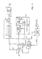
- Figure 2 is a block diagram of a preferred embodiment of the color burst regeneration system of the present invention.
- Referring to Figure 2, a preferred embodiment of the color burst regeneration system includes a digital phase-locked
loop 20, areconstruction unit 22, an analog-to-digital (A/D)converter 24, a random access memory (RAM) 26, anaccess control unit 28, asystem timing unit 30, a digital-to-analog (D/A)converter 32 and alow pass filter 34. The digital phase-lockedloop 20 includes adigital signal processor 36, a D/A converter 38 and a voltage-controlled oscillator (VCXO) 40. - A color
burst information signal 42, such as shown in Figure 1B, is converted to a digital colorburst information signal 44 by the A/D converter 24. The digital phase-lockedloop 20 processes the digital colorburst information signal 44 to provide asystem clock signal 46. Thedigital signal processor 36 compares the pase of thesystem clock signal 46 to the phase of the digital colorburst information signal 44 and generates anerror signal 48 that is converted into avoltage signal 50 by the D/A converter 38. TheVCXO 40 responds to thevoltage signal 50 by generating the system clock signal. THE VCXO 40 defines the frequency of thesystem clock signal 46 to be four times the frequency of the colorburst information signal 42. - The
system clock signal 46 is used to clock the operation of thereconstruction unit 22, the A/D converter 24, the RAMaccess control unit 28, thesystem timing unit 30, the D/A converter 32, and the D/A converter 38. - The RAM
access control unit 28 is clocked by thesystem clock signal 46 for controlling the storage of information in and the retrieval of information from theRAM 26. The RAMaccess control unit 28 causes the digital colorburst information signal 44 to be sampled for storing phase information derived from the colorburst information signal 42 in theRAM 26 four times over each cycle of the colorburst information signal 42. Exemplary sampling points S₁, S₂,... S₈ are shown in Figure 1B. These samples are clocked by thesystem clock signal 42. - The
system timing unit 30 responds to avertical reference signal 52 for determining when during each received scrambled video signal line (Figure 1B) the colorburst information signal 42 should be present and when during each reconstructed video signal line the regenerated color burst signal is to be inserted, and gates the RAMaccess control unit 28 accordingly for controlling when phase information is stored in and retrieved from theRAM 26. - Retrieval of the phase information from the
RAM 26 is gated in advance fo the time when the regenerated color burst signal is to be inserted in each reconstructed video line so as to allow adequate time for regeneration of a standard-length color burst signal. Thereconstruction unit 22 processes the retrieved samples of phase information taken during the less-than-standard-length color burst information signal and extrapolates the sampled phase information over the duration of a standard-length color burst signal. Thereconstruction unit 22 provides a full-length extrapolatedsamples signal 54 to the D/A converter 32 which provides a reconstructed analog colorburst sample signal 56, as shown by the sample points Sn (n=1 to 8) in Figure 1C, to thelow pass filter 34. It should be noted that the signal shown in Figure 1C is not coincident in time with the signal shown in Figure 1B. - The analog color
burst sample signal 56 is passed through thelow pass filter 34 to provide a regenerated sinusoidalcolor burst signal 58, as shown by the sinusoidal waveform in Figure 1C. Thelow pass filter 34 provides a sinusoidal signal from the sample points in thesample signal 56 in accordance with Nyquist's sample theorem, which states that at least two samples per cycle will completely characterize a band-limited signal. - The regenerated standard-length
color burst signal 58 is inserted in the reconstructed video signal at the appropriate time, as shown in Figure 1D.
Claims (5)
means (20, 24) for generating a system clock signal (46) from the color burst information signal (42), with said clock signal having a clock frequency related to and at least twice the given frequency of the color burst information signal;
means (26, 28) for sampling and storing phase information from the color burst information signal, wherein said sampling is clocked by the system clock signal;and
means (22, 32, 34) for regenerating a standard-length color burst signal (58) at the given frequency and in phase with the color burst information signal by retrieving and extrapolating the stored phase information, wherein said retrieval is clocked by the system clock signal.
the phase-locked loop is a digital phase-locked loop (20) :
the system further comprises means (24) for converting the color burst information signal (42) into a digital color burst information signal (44);
the sample and storage means sample the digital color burst information signal (44), and includes a RAM (26) for storing the sampled phase information; and
the color burst signal regeneration means include means (32) for converting the retrieved extrapolated phase information (54) into an analog signal (56).
a low pass filter (34) for generating the color burst signal (58) as a sine wave from the analog signal (56) containing the retrieved and extrapolated phase information.
a low pass filter (34) for generating the color burst signal (58) as a sine wave from the retrieved and extrapolated phase information (56).
Priority Applications (1)
| Application Number | Priority Date | Filing Date | Title |
|---|---|---|---|
| AT87308046T ATE91585T1 (en) | 1986-09-19 | 1987-09-11 | REGENERATION OF THE COLOR SYNCHRONOUS SIGNAL. |
Applications Claiming Priority (2)
| Application Number | Priority Date | Filing Date | Title |
|---|---|---|---|
| US06/909,511 US4719505A (en) | 1986-09-19 | 1986-09-19 | Color burst regeneration |
| US909511 | 1986-09-19 |
Publications (3)
| Publication Number | Publication Date |
|---|---|
| EP0260887A2 true EP0260887A2 (en) | 1988-03-23 |
| EP0260887A3 EP0260887A3 (en) | 1989-08-09 |
| EP0260887B1 EP0260887B1 (en) | 1993-07-14 |
Family
ID=25427350
Family Applications (1)
| Application Number | Title | Priority Date | Filing Date |
|---|---|---|---|
| EP87308046A Expired - Lifetime EP0260887B1 (en) | 1986-09-19 | 1987-09-11 | Colourburst regeneration |
Country Status (11)
| Country | Link |
|---|---|
| US (1) | US4719505A (en) |
| EP (1) | EP0260887B1 (en) |
| JP (1) | JPS63171089A (en) |
| AT (1) | ATE91585T1 (en) |
| AU (1) | AU595930B2 (en) |
| CA (1) | CA1279125C (en) |
| DE (1) | DE3786509T2 (en) |
| DK (1) | DK168977B1 (en) |
| IE (1) | IE61395B1 (en) |
| NO (1) | NO171660C (en) |
| NZ (1) | NZ221796A (en) |
Cited By (1)
| Publication number | Priority date | Publication date | Assignee | Title |
|---|---|---|---|---|
| GB2234123A (en) * | 1989-05-26 | 1991-01-23 | Rca Licensing Corp | Phase locked frequency signal generator |
Families Citing this family (10)
| Publication number | Priority date | Publication date | Assignee | Title |
|---|---|---|---|---|
| JP2655650B2 (en) * | 1987-08-18 | 1997-09-24 | 三菱電機株式会社 | Time axis correction device |
| FR2637757B1 (en) * | 1988-10-11 | 1990-11-16 | Cit Alcatel | METHOD AND DEVICE FOR RECALIBRATING CHROMINANCE SALVES OF A COLOR TELEVISION VIDEO SIGNAL |
| IL96808A (en) * | 1990-04-18 | 1996-03-31 | Rambus Inc | Integrated circuit i/o using a high performance bus interface |
| US6324120B2 (en) | 1990-04-18 | 2001-11-27 | Rambus Inc. | Memory device having a variable data output length |
| US5091936A (en) * | 1991-01-30 | 1992-02-25 | General Instrument Corporation | System for communicating television signals or a plurality of digital audio signals in a standard television line allocation |
| JP2734806B2 (en) * | 1991-06-04 | 1998-04-02 | 松下電器産業株式会社 | Color burst signal phase error detection circuit |
| MY108367A (en) * | 1991-09-30 | 1996-09-30 | Thomson Consumer Electronics S A | Method and apparatus for secure transmisson of video signals. |
| JPH0546190U (en) * | 1991-11-12 | 1993-06-18 | 三洋電機株式会社 | Burst signal continuation circuit |
| US8747472B2 (en) * | 2009-08-14 | 2014-06-10 | Baxano Surgical, Inc. | Spinal therapy device with fixated distraction distance |
| DE102016217683A1 (en) | 2016-09-15 | 2018-03-15 | Tridonic Gmbh & Co. Kg | Synchronization of transmission nodes |
Citations (3)
| Publication number | Priority date | Publication date | Assignee | Title |
|---|---|---|---|---|
| US4291332A (en) * | 1980-04-10 | 1981-09-22 | Tokyo Shibaura Denki Kabushiki Kaisha | Phase-locked circuit |
| US4373168A (en) * | 1979-03-30 | 1983-02-08 | Nippon Electric Co., Ltd. | Digital time-base corrector having a wide correction range |
| EP0127383A1 (en) * | 1983-05-27 | 1984-12-05 | M/A-Com Government Systems, Inc. | Video signal scrambling and descrambling systems |
Family Cites Families (5)
| Publication number | Priority date | Publication date | Assignee | Title |
|---|---|---|---|---|
| JPS57183195A (en) * | 1981-05-07 | 1982-11-11 | Nec Corp | Regenerating circuit for color synchronizing signal |
| JPS58111977A (en) * | 1981-12-25 | 1983-07-04 | ソニー株式会社 | Color display circuit |
| US4626913A (en) * | 1984-06-26 | 1986-12-02 | Rca Corporation | Chroma burst derived clock regenerator for teletext decoder |
| US4679005A (en) * | 1985-01-23 | 1987-07-07 | Sony Corporation | Phase locked loop with frequency offset |
| DE3686439T2 (en) * | 1985-04-12 | 1993-03-04 | Tektronix Inc | DIGITAL PHASE CONTROL LOOP. |
-
1986
- 1986-09-19 US US06/909,511 patent/US4719505A/en not_active Expired - Lifetime
-
1987
- 1987-09-11 DE DE87308046T patent/DE3786509T2/en not_active Expired - Lifetime
- 1987-09-11 AT AT87308046T patent/ATE91585T1/en active
- 1987-09-11 EP EP87308046A patent/EP0260887B1/en not_active Expired - Lifetime
- 1987-09-14 NZ NZ221796A patent/NZ221796A/en unknown
- 1987-09-16 AU AU78458/87A patent/AU595930B2/en not_active Expired
- 1987-09-17 JP JP62233614A patent/JPS63171089A/en active Granted
- 1987-09-17 NO NO873901A patent/NO171660C/en unknown
- 1987-09-17 CA CA000547171A patent/CA1279125C/en not_active Expired - Lifetime
- 1987-09-18 DK DK492487A patent/DK168977B1/en not_active IP Right Cessation
- 1987-09-18 IE IE252787A patent/IE61395B1/en not_active IP Right Cessation
Patent Citations (3)
| Publication number | Priority date | Publication date | Assignee | Title |
|---|---|---|---|---|
| US4373168A (en) * | 1979-03-30 | 1983-02-08 | Nippon Electric Co., Ltd. | Digital time-base corrector having a wide correction range |
| US4291332A (en) * | 1980-04-10 | 1981-09-22 | Tokyo Shibaura Denki Kabushiki Kaisha | Phase-locked circuit |
| EP0127383A1 (en) * | 1983-05-27 | 1984-12-05 | M/A-Com Government Systems, Inc. | Video signal scrambling and descrambling systems |
Cited By (2)
| Publication number | Priority date | Publication date | Assignee | Title |
|---|---|---|---|---|
| GB2234123A (en) * | 1989-05-26 | 1991-01-23 | Rca Licensing Corp | Phase locked frequency signal generator |
| GB2234123B (en) * | 1989-05-26 | 1993-05-05 | Rca Licensing Corp | Frequency locked subcarrier regenerator |
Also Published As
| Publication number | Publication date |
|---|---|
| JPH0355076B2 (en) | 1991-08-22 |
| AU595930B2 (en) | 1990-04-12 |
| DE3786509T2 (en) | 1993-11-18 |
| ATE91585T1 (en) | 1993-07-15 |
| DE3786509D1 (en) | 1993-08-19 |
| CA1279125C (en) | 1991-01-15 |
| JPS63171089A (en) | 1988-07-14 |
| NO873901L (en) | 1988-03-21 |
| DK168977B1 (en) | 1994-07-18 |
| US4719505A (en) | 1988-01-12 |
| NO171660B (en) | 1993-01-04 |
| AU7845887A (en) | 1988-03-24 |
| DK492487D0 (en) | 1987-09-18 |
| IE872527L (en) | 1988-03-19 |
| NO873901D0 (en) | 1987-09-17 |
| DK492487A (en) | 1988-03-20 |
| NO171660C (en) | 1993-04-14 |
| IE61395B1 (en) | 1994-11-02 |
| EP0260887B1 (en) | 1993-07-14 |
| EP0260887A3 (en) | 1989-08-09 |
| NZ221796A (en) | 1989-09-27 |
Similar Documents
| Publication | Publication Date | Title |
|---|---|---|
| EP0260887B1 (en) | Colourburst regeneration | |
| CA1089562A (en) | Television synchronizing apparatus | |
| JP2813106B2 (en) | Transmitter and its operation method | |
| US4231063A (en) | Frame synchronizer having a write-inhibit circuit | |
| CA2007535A1 (en) | Bit synchronizer for short duration burst communications | |
| US4751565A (en) | Microprocessor controlled digital genlock | |
| US6094461A (en) | Data transmission | |
| EP0109551A2 (en) | Apparatus for decoding video address code signals | |
| US5068717A (en) | Method and apparatus for synchronization in a digital composite video system | |
| US4713692A (en) | Method and apparatus for deriving frame interval signals | |
| JPH0548979B2 (en) | ||
| US4639792A (en) | Apparatus for decoding video address code signals | |
| US5006936A (en) | Method and system for high density analog data storage retrieval, and transmission | |
| US4725814A (en) | Method and circuit for analog to digital conversion of a noisy DC voltage signal | |
| US4665444A (en) | Circuit for reproducing video signals | |
| WO1991020124A2 (en) | Digital fm synthesizer for record circuitry | |
| CA2016463C (en) | Phase locked subcarrier regenerator | |
| GB1520311A (en) | Time base compensator | |
| JP3297931B2 (en) | Video signal input device | |
| JPH0681305B2 (en) | Character signal separation and extraction circuit | |
| JPS639395A (en) | Image transmission system | |
| JPH0511833B2 (en) | ||
| JPH08182018A (en) | Television signal transmitter and receiver |
Legal Events
| Date | Code | Title | Description |
|---|---|---|---|
| PUAI | Public reference made under article 153(3) epc to a published international application that has entered the european phase |
Free format text: ORIGINAL CODE: 0009012 |
|
| AK | Designated contracting states |
Kind code of ref document: A2 Designated state(s): AT BE CH DE ES FR GB GR IT LI LU NL SE |
|
| PUAL | Search report despatched |
Free format text: ORIGINAL CODE: 0009013 |
|
| AK | Designated contracting states |
Kind code of ref document: A3 Designated state(s): AT BE CH DE ES FR GB GR IT LI LU NL SE |
|
| 17P | Request for examination filed |
Effective date: 19891031 |
|
| RAP1 | Party data changed (applicant data changed or rights of an application transferred) |
Owner name: CABLE/HOME COMMUNICATION CORP. Owner name: TITAN LINKABIT CORPORATION |
|
| 17Q | First examination report despatched |
Effective date: 19910930 |
|
| RAP1 | Party data changed (applicant data changed or rights of an application transferred) |
Owner name: CABLE/HOME COMMUNICATION CORP. Owner name: THE TITAN CORPORATION |
|
| GRAA | (expected) grant |
Free format text: ORIGINAL CODE: 0009210 |
|
| AK | Designated contracting states |
Kind code of ref document: B1 Designated state(s): AT BE CH DE ES FR GB GR IT LI LU NL SE |
|
| PG25 | Lapsed in a contracting state [announced via postgrant information from national office to epo] |
Ref country code: IT Free format text: LAPSE BECAUSE OF FAILURE TO SUBMIT A TRANSLATION OF THE DESCRIPTION OR TO PAY THE FEE WITHIN THE PRE;WARNING: LAPSES OF ITALIAN PATENTS WITH EFFECTIVE DATE BEFORE 2007 MAY HAVE OCCURRED AT ANY TIME BEFORE 2007. THE CORRECT EFFECTIVE DATE MAY BE DIFFERENT FROM THE ONE RECORDED.SCRIBED TIME-LIMIT Effective date: 19930714 Ref country code: AT Effective date: 19930714 Ref country code: SE Effective date: 19930714 Ref country code: LI Effective date: 19930714 Ref country code: GR Free format text: LAPSE BECAUSE OF FAILURE TO SUBMIT A TRANSLATION OF THE DESCRIPTION OR TO PAY THE FEE WITHIN THE PRESCRIBED TIME-LIMIT Effective date: 19930714 Ref country code: CH Effective date: 19930714 Ref country code: BE Effective date: 19930714 Ref country code: NL Effective date: 19930714 |
|
| REF | Corresponds to: |
Ref document number: 91585 Country of ref document: AT Date of ref document: 19930715 Kind code of ref document: T |
|
| REF | Corresponds to: |
Ref document number: 3786509 Country of ref document: DE Date of ref document: 19930819 |
|
| PG25 | Lapsed in a contracting state [announced via postgrant information from national office to epo] |
Ref country code: ES Free format text: LAPSE BECAUSE OF FAILURE TO SUBMIT A TRANSLATION OF THE DESCRIPTION OR TO PAY THE FEE WITHIN THE PRESCRIBED TIME-LIMIT Effective date: 19931025 |
|
| REG | Reference to a national code |
Ref country code: CH Ref legal event code: PL |
|
| ET | Fr: translation filed | ||
| NLV1 | Nl: lapsed or annulled due to failure to fulfill the requirements of art. 29p and 29m of the patents act | ||
| PLBE | No opposition filed within time limit |
Free format text: ORIGINAL CODE: 0009261 |
|
| STAA | Information on the status of an ep patent application or granted ep patent |
Free format text: STATUS: NO OPPOSITION FILED WITHIN TIME LIMIT |
|
| 26N | No opposition filed | ||
| REG | Reference to a national code |
Ref country code: GB Ref legal event code: 732E |
|
| PGFP | Annual fee paid to national office [announced via postgrant information from national office to epo] |
Ref country code: LU Payment date: 19980908 Year of fee payment: 12 |
|
| PG25 | Lapsed in a contracting state [announced via postgrant information from national office to epo] |
Ref country code: LU Free format text: LAPSE BECAUSE OF NON-PAYMENT OF DUE FEES Effective date: 19990911 |
|
| REG | Reference to a national code |
Ref country code: GB Ref legal event code: IF02 |
|
| PGFP | Annual fee paid to national office [announced via postgrant information from national office to epo] |
Ref country code: GB Payment date: 20060829 Year of fee payment: 20 |
|
| PGFP | Annual fee paid to national office [announced via postgrant information from national office to epo] |
Ref country code: DE Payment date: 20060925 Year of fee payment: 20 |
|
| REG | Reference to a national code |
Ref country code: GB Ref legal event code: PE20 |
|
| PG25 | Lapsed in a contracting state [announced via postgrant information from national office to epo] |
Ref country code: GB Free format text: LAPSE BECAUSE OF EXPIRATION OF PROTECTION Effective date: 20070910 |
|
| PGFP | Annual fee paid to national office [announced via postgrant information from national office to epo] |
Ref country code: FR Payment date: 20060929 Year of fee payment: 20 |
|
| P01 | Opt-out of the competence of the unified patent court (upc) registered |
Effective date: 20230520 |