EP0258721A1 - Method and device for drop-out compensation at the reproduction of magnetically registered signals - Google Patents
Method and device for drop-out compensation at the reproduction of magnetically registered signals Download PDFInfo
- Publication number
- EP0258721A1 EP0258721A1 EP87111867A EP87111867A EP0258721A1 EP 0258721 A1 EP0258721 A1 EP 0258721A1 EP 87111867 A EP87111867 A EP 87111867A EP 87111867 A EP87111867 A EP 87111867A EP 0258721 A1 EP0258721 A1 EP 0258721A1
- Authority
- EP
- European Patent Office
- Prior art keywords
- signal
- time
- dropout
- identification signal
- channel
- Prior art date
- Legal status (The legal status is an assumption and is not a legal conclusion. Google has not performed a legal analysis and makes no representation as to the accuracy of the status listed.)
- Granted
Links
Images
Classifications
-
- H—ELECTRICITY
- H04—ELECTRIC COMMUNICATION TECHNIQUE
- H04N—PICTORIAL COMMUNICATION, e.g. TELEVISION
- H04N5/00—Details of television systems
- H04N5/76—Television signal recording
- H04N5/91—Television signal processing therefor
- H04N5/93—Regeneration of the television signal or of selected parts thereof
- H04N5/94—Signal drop-out compensation
- H04N5/945—Signal drop-out compensation for signals recorded by pulse code modulation
-
- G—PHYSICS
- G11—INFORMATION STORAGE
- G11B—INFORMATION STORAGE BASED ON RELATIVE MOVEMENT BETWEEN RECORD CARRIER AND TRANSDUCER
- G11B20/00—Signal processing not specific to the method of recording or reproducing; Circuits therefor
- G11B20/10—Digital recording or reproducing
- G11B20/18—Error detection or correction; Testing, e.g. of drop-outs
Definitions
- the invention relates to a method and a device for dropout compensation in the reproduction of magnetically recorded signals with the features specified in the preamble of claim 1 and claim 7, respectively.
- a circuit for dropout compensation is usually used when playing back magnetically recorded signals. Using this, signal failures in the reproduced signal are recognized and replaced by information from previous signal sections which have been buffered in a dropout memory.
- the dropout compensation can either take place in the signal with a time error or in the time error correction by making use of the memory arrangement which is present anyway.
- the invention is based on the object of specifying a method by means of which dropout compensation can also take place if, in the event of a dropout, information from another channel is to be used instead of the disturbed information.
- Claims 2 to 6 relate to advantageous refinements of the method specified in claim 1.
- Claims 7 to 12 describe a device for dropout compensation according to the present invention.
- the advantages of the invention consist, in particular, in that a correctly timed identification signal is made available at the output of the memory arrangement used for time error correction, without the need for transmission of the identification signal additional storage space is required.
- This identification signal is evaluated and used to control the dropout memory. Further advantageous properties result from an exemplary embodiment which is explained in more detail below with reference to the (single) figure.
- a broadband video signal is recorded in such a way that successive sections of information are assigned adjacent helical tracks of a magnetic tape.
- the successive lines of a broadband video signal for example, can be fed to different storage elements of a memory on the recording side and can be time-expanded there. These time-expanded signals are distributed over the two helical tracks mentioned.
- Such a recording method, from which the invention is based, is described, for example, in the aforementioned German patent application P 36 13 798, which has not been published previously.
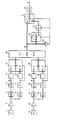
- Such signals are reproduced by the playback heads 1 and 2 (see figure).
- the reproduced signals which are subject to different time errors, are amplified in reproduction amplifiers 2 (or 12).
- the amplified signals arrive on the one hand Demodulators 3 (or 13) and on the other hand on dropout detectors 6 (or 16).
- the demodulated signals are digitized in analog-digital converters 4 (or 14) or converted into an 8-bit data stream.
- the 8-bit data stream is checked in a circuit 5 (or 15) to determine whether a certain predetermined bit combination occurs or not. For example, the bit stream can be checked to see whether all bits are set.
- the LSB Least Significant Bit
- bit stream arrives unchanged at the output of circuit 5 (or 15).
- the dropout detectors 6 check the reproduced signal - for example by evaluating the envelope in the case of a frequency-modulated reproduction signal - for dropouts and each generate an identification signal which provides information as to whether a dropout is present or not.
- This identification signal is passed through a delay element 7 (or 17) in order to compensate for the delay to which the reproduced signal is subjected by the demodulation and the A / D conversion.
- the delayed identification signal is used on the one hand to control the switch 9 (or 19).
- the switch 9 (or 19) When the signal is undisturbed, the switch 9 (or 19) is in the switching position a, so that the switch is transparent to the output signal of the circuit 5 (or 15).
- the switch In the case of a dropout, the switch is placed in its switching position b, so that the switch is transparent to the output signal of a circuit 8 (or 18).
- the circuit 8 (or 18) generates the reserved bit combination in the event of a dropout. This is passed on via switch 9 (or 19) and thus inserted into the digital video signal.
- the output signals of the switches 9 are fed to a circuit 20 in which the signals are time-transformed, time-corrected and combined to form a single-channel signal.
- a circuit 20 in which the signals are time-transformed, time-corrected and combined to form a single-channel signal.
- Such Circuitry is described, for example, in the above-mentioned German patent application P 36 13 798, which has not been published beforehand, and can consist of a memory with several memory elements (RAM's) and a multiplexer.
- a single-channel, time error-corrected 8-bit data stream is present at the output of the circuit 20. This is fed to the contact a of a switch 21, the contact c of a switch 23 and a circuit 25 for evaluating the time-corrected data stream.
- Circuit 25 can be an AND gate, for example, if the reserved bit combination consists exclusively of "ones".
- the output signal of the AND gate 25 is fed to the respective control inputs of a switch 23, a dropout memory 24 and a further switch 21.
- the switch 23 When the signal is undisturbed, the switch 23 is in its switching position b and the switch 21 is in the switching position a. Consequently, the undisturbed time error-corrected signal present at the output of the circuit 20 reaches the output A of the circuit via the switch 21 and the D / A converter 22.
- the undisturbed time error-corrected signal present at the output of the circuit 20 reaches the dropout memory 24 via the switch 23 and is stored there.
- the switch 23 In the case of a dropout, the switch 23 is in its switch position a and the switch 21 is in the switch position b. Consequently, the disturbed time error corrected signal present at the output of the circuit 20 is separated both from the output A of the overall circuit and from the dropout memory 24. Instead, a signal stored in the dropout memory 24 reaches the output A of the circuit via the switch 21 and the D / A converter 22.
- the reproduced time-error signal of each channel is therefore checked for dropouts prior to demodulation, and an identification signal is generated for each channel.
- a bit combination which corresponds to a specific resolution level or bit combination of the digital video signal, is assigned to this identification signal.
- a circuit is provided in the path of the digital video signal which precludes this particular bit combination from occurring in the video signal. If there is a dropout, the key signal is keyed into the video signal and subjected to the time error correction. After the time error correction there is a timely identification signal available, which can be used to control the dropout memory or dropout process.
- An advantageous development of the invention consists in reserving further bit combinations of the time-error signal for the transmission of any additional information. It is only necessary to ensure that bit combinations that occur rarely, preferably at the edge of the modulation range, are used.
Landscapes
- Engineering & Computer Science (AREA)
- Signal Processing (AREA)
- Multimedia (AREA)
- Television Signal Processing For Recording (AREA)
- Signal Processing For Digital Recording And Reproducing (AREA)
Abstract
Description
Die Erfindung betrifft ein Verfahren und eine Einrichtung zur Dropoutkompensation bei der Wiedergabe magnetisch aufgezeichneter Signale mit den im Oberbegriff des Anspruchs 1 bzw. Anspruchs 7 angegebenen Merkmalen.The invention relates to a method and a device for dropout compensation in the reproduction of magnetically recorded signals with the features specified in the preamble of claim 1 and
Bei der Wiedergabe magnetisch aufgezeichneter Signale wird üblicherweise eine Schaltung zur Dropoutkompensation verwendet. Mittels dieser werden Signalausfälle im wiedergegebenen Signal erkannt und durch Informationen vorheriger Signalabschnitte ersetzt, welche in einem Dropoutspeicher zwischengespeichert wurden. Die Dropoutkompensation kann entweder im zeitfehlerbehafteten Signal erfolgen oder aber bei der Zeitfehlerkorrektur durch Mitausnutzung der ohnehin vorhandenen Speicheranordnung.A circuit for dropout compensation is usually used when playing back magnetically recorded signals. Using this, signal failures in the reproduced signal are recognized and replaced by information from previous signal sections which have been buffered in a dropout memory. The dropout compensation can either take place in the signal with a time error or in the time error correction by making use of the memory arrangement which is present anyway.
Diese bekannten Verfahren sind allerdings nicht anwendbar, wenn eine mehrkanalige Aufzeichnung vorliegt (siehe beispielsweise nicht vorveröffentlichte Patentanmeldung P 36 13 798 vom 24.04.86) und im Dropoutfall eine Information aus einem anderen Kanal anstelle der gestörten Information eingesetzt werden soll, da die aus verschiedenen Spuren wiedergegebenen Signale unterschiedliche Zeitfehler aufweisen. Eine Dropoutkompensation kann in diesem Fall nur nach der Zeitfehlerkorrektur erfolgen.However, these known methods cannot be used if there is multichannel recording (see, for example, unpublished patent application P 36 13 798 from April 24, 1986) and in the event of a dropout, information from another channel is to be used instead of the disturbed information, since it consists of different tracks reproduced signals have different timing errors. In this case, dropout compensation can only take place after the time error correction.
Der Erfindung liegt die Aufgabe zugrunde, ein Verfahren anzugeben, mittels dessen eine Dropoutkompensation auch dann erfolgen kann, wenn im Dropoutfall eine Information aus einem anderen Kanal anstelle der gestörten Information eingesetzt werden soll.The invention is based on the object of specifying a method by means of which dropout compensation can also take place if, in the event of a dropout, information from another channel is to be used instead of the disturbed information.
Diese Aufgabe wird durch die im kennzeichnenden Teil des Anspruchs 1 angegebenen Merkmale gelöst. Die Ansprüche 2 bis 6 betreffen vorteilhafte Ausgestaltungen des im Anspruch 1 angegebenen Verfahrens. Die Ansprüche 7 bis 12 beschreiben eine Einrichtung zur Dropout-Kompensation nach der vorliegenden Erfindung.This object is achieved by the features specified in the characterizing part of claim 1.
Die Vorteile der Erfindung bestehen insbesondere darin, daß am Ausgang der zur Zeitfehlerkorrektur verwendeten Speicheranordnung ein zeitlich richtiges Kennsignal zur Verfügung gestellt wird, ohne daß zur Übertragung des Kennsignals zusätzlicher Speicherplatz benötigt wird. Dieses Kennsignal wird ausgewertet und zur Steuerung des Dropoutspeichers verwendet. Weitere vorteilhafte Eigenschaften ergeben sich aus einem Ausführungsbeispiel, welches im folgenden anhand der (einzigen) Figur näher erläutert wird.The advantages of the invention consist, in particular, in that a correctly timed identification signal is made available at the output of the memory arrangement used for time error correction, without the need for transmission of the identification signal additional storage space is required. This identification signal is evaluated and used to control the dropout memory. Further advantageous properties result from an exemplary embodiment which is explained in more detail below with reference to the (single) figure.
Ein breitbandiges Videosignal sei derart aufgezeichnet, daß aufeinanderfolgende Informationsabschnitte nebeneinanderliegenden Schrägspuren eines Magnetbandes zugeordnet sind. Um dies zu erreichen, können beispielsweise aufzeichnungsseitig die aufeinanderfolgenden Zeilen eines breitbandigen Videosignals unterschiedlichen Speicherelementen eines Speichers zugeführt und dort zeitexpandiert werden. Diese zeitexpandierten Signale werden auf die beiden genannten Schrägspuren verteilt. Ein solches Aufzeichnungsverfahren, von dem die Erfindung ausgeht, ist beispielsweise in der bereits oben genannten nicht vorveröffentlichten deutschen Patentanmeldung P 36 13 798 beschrieben.A broadband video signal is recorded in such a way that successive sections of information are assigned adjacent helical tracks of a magnetic tape. To achieve this, the successive lines of a broadband video signal, for example, can be fed to different storage elements of a memory on the recording side and can be time-expanded there. These time-expanded signals are distributed over the two helical tracks mentioned. Such a recording method, from which the invention is based, is described, for example, in the aforementioned German patent application P 36 13 798, which has not been published previously.
Bei der Wiedergabe werden derartige Signale von den Wiedergabeköpfen 1 und 2 wiedergegeben (siehe Figur). Die wiedergegebenen Signale, die unterschiedlich zeitfehlerbehaftet sind, werden in Wiedergabeverstärkern 2 (bzw. 12) verstärkt. Die verstärkten Signale gelangen einerseits an Demodulatoren 3 (bzw. 13) und andererseits an Dropoutdetektoren 6 (bzw. 16). Die demodulierten Signale werden in Analog-Digital-Wandlern 4 (bzw. 14) digitalisiert bzw. in einen 8-Bit-Datenstrom umgewandelt.During playback, such signals are reproduced by the playback heads 1 and 2 (see figure). The reproduced signals, which are subject to different time errors, are amplified in reproduction amplifiers 2 (or 12). The amplified signals arrive on the one hand Demodulators 3 (or 13) and on the other hand on dropout detectors 6 (or 16). The demodulated signals are digitized in analog-digital converters 4 (or 14) or converted into an 8-bit data stream.
Mittels dieses 8-Bit Datenstroms können insgesamt 2⁸ = 256 verschiedene Auflösungsstufen dargestellt werden. In einer Schaltung 5 (bzw. 15) wird der 8-Bit-Datenstrom daraufhin überprüft, ob eine bestimmte vorgegebene Bitkombination auftritt oder nicht Beispielsweise kann der Bitstrom daraufhin überprüft werden, ob alle Bits gesetzt sind.Using this 8-bit data stream, a total of 2⁸ = 256 different resolution levels can be displayed. The 8-bit data stream is checked in a circuit 5 (or 15) to determine whether a certain predetermined bit combination occurs or not. For example, the bit stream can be checked to see whether all bits are set.
Ist das der Fall, dan wird das LSB (Least Significant Bit) zu Null gesetzt. Damit ist sichergestellt, daß am Ausgang der Schaltung 5 (bzw. 15) niemals alle Bits gesetzt sind. Dies bewirkt letztendlich eine Verringerung der Signalauflösung von 256 Auflösungsstufen um eine auf 255 Auflösungsstufen. Diese geringfügige Verringerung der Auflösung kann vom menschlichen Auge nicht wahrgenommen werden, da die fehlende Auflösungsstufe am Rande des Aussteuerungsbereiches liegt.If this is the case, the LSB (Least Significant Bit) is set to zero. This ensures that all bits are never set at the output of circuit 5 (or 15). This ultimately causes the signal resolution to be reduced from 256 resolution levels by one to 255 resolution levels. This slight reduction in resolution cannot be perceived by the human eye, since the missing resolution level lies on the edge of the modulation range.
Sind nicht alle Bits gesetzt, dann gelangt der Bitstrom unverändert an den Ausgang der Schaltung 5 (bzw. 15).If not all bits are set, the bit stream arrives unchanged at the output of circuit 5 (or 15).
Die Dropoutdetektoren 6 (bzw. 16) überprüfen das wiedergegebene Signal - beispielsweise durch Auswertung der Hüllkurve im Falle eines frequenzmodulierten Wiedergabesignals - auf Dropouts und erzeugen je ein Kennsignal, welches Auskunft darüber gibt, ob ein Dropout vorliegt oder nicht. Dieses Kennsignal wird über ein Verzögerungsglied 7 (bzw. 17) geleitet, um diejenige Verzögerung zu kompensieren, welcher das wiedergegebene Signal durch die Demodulation und die A/D-Wandlung unterworfen ist.The dropout detectors 6 (or 16) check the reproduced signal - for example by evaluating the envelope in the case of a frequency-modulated reproduction signal - for dropouts and each generate an identification signal which provides information as to whether a dropout is present or not. This identification signal is passed through a delay element 7 (or 17) in order to compensate for the delay to which the reproduced signal is subjected by the demodulation and the A / D conversion.
Das verzögerte Kennsignal wird einerseits verwendet, um den Schalter 9 (bzw. 19) zu steuern. Bei ungestörte Signal befindet sich der Schalter 9 (bzw. 19) in der Schaltstellung a, so daß der Schalter für das Ausgangssignal der Schaltung 5 (bzw. 15) durchlässig ist. Im Falle eines Dropouts wird der Schalter in seine Schaltstellung b gelegt, so daß der Schalter für das Ausgangssignal einer Schaltung 8 (bzw. 18) durchlässig ist. Die Schaltung 8 (bzw. 18) erzeugt im Falle eines Dropouts die reservierte Bitkombination. Diese wird über den Schalter 9 (bzw. 19) weitergegeben und damit in das digitale Videosignal eingesetzt.The delayed identification signal is used on the one hand to control the switch 9 (or 19). When the signal is undisturbed, the switch 9 (or 19) is in the switching position a, so that the switch is transparent to the output signal of the circuit 5 (or 15). In the case of a dropout, the switch is placed in its switching position b, so that the switch is transparent to the output signal of a circuit 8 (or 18). The circuit 8 (or 18) generates the reserved bit combination in the event of a dropout. This is passed on via switch 9 (or 19) and thus inserted into the digital video signal.
Die Ausgangssignale der Schalter 9 (bzw. 19) werden einer Schaltung 20 zugeführt, in der die Signale zeittransformiert, zeitfehlerkorrigiert und zu einem einkanaligen Signal zusammengefäßt werden. Eine solche Schaltung ist beispielsweise in der oben genannten nicht vorveröffentlichten deutschen Patentanmeldung P 36 13 798 beschrieben und kann aus einem Speicher mit mehreren Speicherelementen (RAM's) und einem Multiplexer bestehen.The output signals of the switches 9 (or 19) are fed to a
Am Ausgang der Schaltung 20 liegt ein einkanaliger, zeitfehlerkorrigierter 8-Bit-Datenstrom an. Dieser wird dem Kontakt a eines Schalters 21, dem Kontakt c eines Schalters 23 und einer Schaltung 25 zur Auswertung des zeitfehler korrigierten Datenstroms zugeführt.A single-channel, time error-corrected 8-bit data stream is present at the output of the
Die Schaltung 25 kann beispielsweise dann - wenn die reservierte Bitkombination ausschließlich aus "Einsen" besteht - ein UND-Gatter sein.
Das Ausgangssignal des UND-Gatters 25 wird den jeweiligen Steuereingängen eines Schalters 23, eines Dropoutspeichers 24 und eines weiteren Schalters 21 zugeführt.The output signal of the
Bei ungestörtem Signal befindet sich der Schalter 23 in seiner Schaltstellung b und der Schalter 21 in der Schaltstellung a. Folglich gelangt das ungestörte, am Ausgang der Schaltung 20 anliegende zeitfehlerkorrigierte Signal über den Schalter 21 und den D/A-Wandler 22 an den Ausgang A der Schaltung.When the signal is undisturbed, the
Ferner gelangt das ungestörte, am Ausgang der Schaltung 20 anliegende zeitfehlerkorrigierte Signal über den Schalter 23 in den Dropoutspeicher 24 und wird dort abgespeichert.Furthermore, the undisturbed time error-corrected signal present at the output of the
Im Falle eines Dropouts befindet sich der Schalter 23 in seiner Schaltstellung a und der Schalter 21 in der Schaltstellung b. Folglich ist das gestörte, am Ausgang der Schaltung 20 anliegende zeitfehlerkorrigierte Signal sowohl vom Ausgang A der Gesamtschaltung als auch vom Dropoutspeicher 24 abgetrennt. Stattdessen gelangt ein im Dropoutspeicher 24 abgespeichertes Signal über den Schalter 21 und den D/A-Wandler 22 an den Ausgang A der Schaltung.In the case of a dropout, the
Mittels der beschriebenen Einrichtung wird demnach das wiedergegebene zeitfehlerbehaftete Signal eines jeden Kanals vor der Demodulation auf Dropouts hin überprüft und je Kanal ein Kennsignal erzeugt. Diesem Kennsignal wird eine Bitkombination zugeordnet, welche einer bestimmten Auflösungsstufe bzw. Bitkombination des digitalen Videosignals entspricht. Im Weg des digitalen Videosignals ist eine Schaltung vorgesehen, die ausschließt, daß diese bestimmte Bitkombination im Videosignal auftritt. Das Kenssignal wird bei Vorliegen eines Dropouts in das Videosignal eingetastet und mit diesem der Zeitfehlerkorrektur unterworfen. Nach der Zeitfehlerkorrektur steht ein zeitrichtiges Kennsignal zur Verfügung, welches zur Steuerung des Dropoutspeichers bzw. Dropoutvorgangs verwendet werden kann.Using the described device, the reproduced time-error signal of each channel is therefore checked for dropouts prior to demodulation, and an identification signal is generated for each channel. A bit combination, which corresponds to a specific resolution level or bit combination of the digital video signal, is assigned to this identification signal. A circuit is provided in the path of the digital video signal which precludes this particular bit combination from occurring in the video signal. If there is a dropout, the key signal is keyed into the video signal and subjected to the time error correction. After the time error correction there is a timely identification signal available, which can be used to control the dropout memory or dropout process.
Eine vorteilhafte Weiterbildung der Erfindung besteht darin, weitere Bitkombinationen des zeitfehlerbehafteten Signals zur Übertragung beliebiger Zusatzinformationen zu reservieren. Es muß lediglich darauf geachtet werden, daß selten auftretende Bitkombinationen, vorzugsweise am Rande des Aussteuerungsbereiches, verwendet werden.An advantageous development of the invention consists in reserving further bit combinations of the time-error signal for the transmission of any additional information. It is only necessary to ensure that bit combinations that occur rarely, preferably at the edge of the modulation range, are used.
Claims (12)
- die Signale in digitaler Form zeitfehlerkorrigiert und zu einem einkanaligen Signal zusammengefaßt werden, und
- im Dropoutfall das Ausgangssignal eines Dropout-Speichers als Ersatz für den gestörten Signalabschnitt in das einkanalige, zeitfehlerkorrigierte Signal eingesetzt wird,
dadurch gekennzeichnet, daß - in jedem Kanal mindestens eine Bitkombination des zeitfehlerbehafteten digitalen Signals zur Übertragung des Kennsignals reserviert,
- das Kennsignal zusammen mit dem zeitfehlerbehafteten Signal zeitfehlerkorrigiert und
- das zeitfehlerkorrigierte Kennsignal zur Steuerung des Dropoutspeichers verwendet wird.1. Method for dropout compensation in the reproduction of magnetically recorded signals which are reproduced from several tracks of a recording medium, in which an identification signal is generated in each channel by evaluating the reproduced signal, which indicates whether a dropout is present or not,
- The signals are time-corrected in digital form and combined to form a single-channel signal, and
in the event of a dropout, the output signal of a dropout memory is used as a replacement for the disturbed signal section in the single-channel, time error-corrected signal,
characterized in that - reserves in each channel at least one bit combination of the digital signal, which is subject to time errors, for the transmission of the identification signal,
- The identification signal together with the time error-corrected signal and time error corrected
- The time error corrected identification signal is used to control the dropout memory.
- einem Dropoutdetektor in jedem Kanal, welcher das wiedergegebene zeitfehlerbehaftete Signal auf Dropouts hin überprüft und ein Kennsignal erzeugt,
- einer Schaltung zur Zeitfehlerkorrektur, welcher die wiedergegebenen Signale in digitaler Form als Bitströme zugeführt werden,
- einer Schaltung zur Zusammenfassung des mehrkanaligen Signals in ein einkanaliges Signal, und
- einem Dropoutspeicher, dessen Ausgangssignal im Dropoutfall in das einkanalige Signal eingetastet wird,
gekennzeichnet durch
- in jedem kanal angeordnete Schaltungen (5, 15), welche mindestens eine Bitkombination des jeweiligen zeitfehlerbehafteten Bitstrom zur Übertragung des Kennsignals reservieren,
- in jedem Kanal angeordnete Schaltungen (9, 19) zur Eintastung des Kennsignals in den jeweiligen zeitfehlerbehafteten Bitstrom, und
- eine Schaltung (25) zur Auswertung des zeitfehlerkorrigierten Kennsignals, deren Ausgangssignal zur Steuerung des Dropoutspeichers verwendet wird.7. Device for dropout compensation when playing back magnetically recorded signals, which are reproduced from several tracks of a recording medium, with
a dropout detector in each channel, which checks the reproduced time-error signal for dropouts and generates an identification signal,
a circuit for time error correction, to which the reproduced signals are supplied in digital form as bit streams,
a circuit for combining the multi-channel signal into a single-channel signal, and
a dropout memory whose output signal is keyed into the single-channel signal in the event of a dropout,
marked by
- Circuits (5, 15) arranged in each channel, which reserve at least one bit combination of the respective time-error bit stream for the transmission of the identification signal,
- In each channel arranged circuits (9, 19) for keying the identification signal in the respective time-error bit stream, and
- A circuit (25) for evaluating the time error corrected identification signal, the output signal of which is used to control the dropout memory.
Priority Applications (1)
| Application Number | Priority Date | Filing Date | Title |
|---|---|---|---|
| AT87111867T ATE68286T1 (en) | 1986-09-04 | 1987-08-17 | METHOD AND DEVICE FOR DROPOUT COMPENSATION WHEN REPLAYING MAGNETICALLY RECORDED SIGNALS. |
Applications Claiming Priority (2)
| Application Number | Priority Date | Filing Date | Title |
|---|---|---|---|
| DE3630179 | 1986-09-04 | ||
| DE19863630179 DE3630179A1 (en) | 1986-09-04 | 1986-09-04 | METHOD AND DEVICE FOR DROPOUT COMPENSATION IN THE REPRODUCTION OF MAGNETICALLY RECORDED SIGNALS |
Publications (2)
| Publication Number | Publication Date |
|---|---|
| EP0258721A1 true EP0258721A1 (en) | 1988-03-09 |
| EP0258721B1 EP0258721B1 (en) | 1991-10-09 |
Family
ID=6308945
Family Applications (1)
| Application Number | Title | Priority Date | Filing Date |
|---|---|---|---|
| EP87111867A Expired - Lifetime EP0258721B1 (en) | 1986-09-04 | 1987-08-17 | Method and device for drop-out compensation at the reproduction of magnetically registered signals |
Country Status (5)
| Country | Link |
|---|---|
| US (1) | US4812925A (en) |
| EP (1) | EP0258721B1 (en) |
| JP (1) | JPS63133361A (en) |
| AT (1) | ATE68286T1 (en) |
| DE (2) | DE3630179A1 (en) |
Families Citing this family (5)
| Publication number | Priority date | Publication date | Assignee | Title |
|---|---|---|---|---|
| JPH0773363B2 (en) * | 1988-01-21 | 1995-08-02 | パイオニア株式会社 | Signal reproduction processor |
| NL8801206A (en) * | 1988-05-09 | 1989-12-01 | Philips Nv | DROP-OUT COMPENSATION CIRCUIT. |
| EP0398651B1 (en) * | 1989-05-16 | 1997-04-23 | Canon Kabushiki Kaisha | Device for processing transmitted digital video signal |
| DE4103974A1 (en) * | 1991-02-09 | 1992-08-13 | Thomson Brandt Gmbh | OPTICAL RECORDING AND / OR PLAYBACK DEVICE |
| JP2688725B2 (en) * | 1991-05-07 | 1997-12-10 | シャープ株式会社 | Video signal recording and playback device |
Citations (4)
| Publication number | Priority date | Publication date | Assignee | Title |
|---|---|---|---|---|
| EP0132086A2 (en) * | 1983-07-19 | 1985-01-23 | Sony Corporation | Methods of and apparatus for correcting errors in binary data |
| EP0149245A2 (en) * | 1983-12-26 | 1985-07-24 | Hitachi, Ltd. | PCM data recording system |
| EP0170328A1 (en) * | 1984-08-02 | 1986-02-05 | Koninklijke Philips Electronics N.V. | Device for correcting and concealing errors in a data stream, and video and/or audio reproduction apparatus comprising such a device |
| EP0198702A2 (en) * | 1985-04-13 | 1986-10-22 | Sony Corporation | Methods of correcting errors in digital data |
Family Cites Families (2)
| Publication number | Priority date | Publication date | Assignee | Title |
|---|---|---|---|---|
| US4541018A (en) * | 1981-11-06 | 1985-09-10 | Victor Company Of Japan, Ltd. | Dropout compensation and chrominance subcarrier frequency conversion circuit in a video signal reproducing apparatus |
| DE3613798A1 (en) * | 1986-04-24 | 1987-10-29 | Grundig Emv | METHOD FOR PROCESSING TELEVISION SIGNALS |
-
1986
- 1986-09-04 DE DE19863630179 patent/DE3630179A1/en not_active Withdrawn
-
1987
- 1987-08-17 AT AT87111867T patent/ATE68286T1/en active
- 1987-08-17 DE DE8787111867T patent/DE3773594D1/en not_active Expired - Lifetime
- 1987-08-17 EP EP87111867A patent/EP0258721B1/en not_active Expired - Lifetime
- 1987-09-01 JP JP62216556A patent/JPS63133361A/en active Pending
- 1987-09-02 US US07/092,338 patent/US4812925A/en not_active Expired - Fee Related
Patent Citations (4)
| Publication number | Priority date | Publication date | Assignee | Title |
|---|---|---|---|---|
| EP0132086A2 (en) * | 1983-07-19 | 1985-01-23 | Sony Corporation | Methods of and apparatus for correcting errors in binary data |
| EP0149245A2 (en) * | 1983-12-26 | 1985-07-24 | Hitachi, Ltd. | PCM data recording system |
| EP0170328A1 (en) * | 1984-08-02 | 1986-02-05 | Koninklijke Philips Electronics N.V. | Device for correcting and concealing errors in a data stream, and video and/or audio reproduction apparatus comprising such a device |
| EP0198702A2 (en) * | 1985-04-13 | 1986-10-22 | Sony Corporation | Methods of correcting errors in digital data |
Also Published As
| Publication number | Publication date |
|---|---|
| US4812925A (en) | 1989-03-14 |
| EP0258721B1 (en) | 1991-10-09 |
| JPS63133361A (en) | 1988-06-06 |
| DE3630179A1 (en) | 1988-03-10 |
| DE3773594D1 (en) | 1991-11-14 |
| ATE68286T1 (en) | 1991-10-15 |
Similar Documents
| Publication | Publication Date | Title |
|---|---|---|
| DE3102967C2 (en) | ||
| DE2147512C3 (en) | Method for recording and retrieving individual images with associated sound information | |
| EP0276753B1 (en) | Method and apparatus for transmitting digital information and/or for recording and reproducing | |
| DE2938503A1 (en) | METHOD AND DEVICE FOR RECORDING AND PLAYING BACK AUDIO SIGNALS WITH DIGITAL RECORDING | |
| DE3142355C2 (en) | Method and circuit arrangement for determining a control signal assigned to a digital data signal | |
| DE3115902A1 (en) | DIGITAL VIDEO DATA RECORDING AND / OR PLAYBACK DEVICE | |
| DE2513922C3 (en) | Arrangement for reducing information loss as a result of recording medium defects in a PCM storage device | |
| DE2944403C2 (en) | ||
| DE3916592A1 (en) | PCM SIGNAL GENERATION / PLAYBACK DEVICE | |
| DE2901034B2 (en) | Method and circuit arrangement for the compression and decompression of analog signals in digital form | |
| DE3048692C2 (en) | ||
| EP0262362B1 (en) | Method for recording and reproducing data packets transmitted with a television signal | |
| EP0258721B1 (en) | Method and device for drop-out compensation at the reproduction of magnetically registered signals | |
| DE3150365A1 (en) | METHOD AND DEVICE FOR CORRECTING ERRORS IN DIGITAL DATA | |
| DE3108941A1 (en) | ARRANGEMENT FOR PREVENTING ERROR CORRECTIONS | |
| DE2758230B2 (en) | Signal transmission system for differential pulse code modulated (DPCM) signals | |
| DE1202315B (en) | Circuit arrangement for reproducing video signals stored on magnetic tape | |
| DE3238119A1 (en) | ARRANGEMENTS FOR DIGITAL CODING AND DECODING OF RECORDING SIGNALS | |
| DE3737056C2 (en) | ||
| DE2130946B2 (en) | Magnetic tape recorder for selective recording and playback of information signals | |
| DE3114451A1 (en) | "RECORDING SCHEME FOR EASIER ERROR COVERAGE AND CORRESPONDING RECORDING AND / OR REPRODUCTION DEVICE" | |
| EP0226796B1 (en) | Video recording apparatus for a high resolution television system | |
| DE3044623A1 (en) | Magnetic tape recording of digital signals - has multiplexing of signals to number of pick=ups to optimise data recording | |
| DE3744077A1 (en) | ARRANGEMENT FOR PLAYING AUDIO SIGNALS | |
| DE3222604A1 (en) | METHOD FOR TRANSMITTING SEVERAL TYPES OF INFORMATION ABOUT A TELEVISION CHANNEL AND DEVICE FOR IMPLEMENTING THE SAME |
Legal Events
| Date | Code | Title | Description |
|---|---|---|---|
| PUAI | Public reference made under article 153(3) epc to a published international application that has entered the european phase |
Free format text: ORIGINAL CODE: 0009012 |
|
| AK | Designated contracting states |
Kind code of ref document: A1 Designated state(s): AT DE FR GB |
|
| 17P | Request for examination filed |
Effective date: 19880907 |
|
| 17Q | First examination report despatched |
Effective date: 19900102 |
|
| GRAA | (expected) grant |
Free format text: ORIGINAL CODE: 0009210 |
|
| AK | Designated contracting states |
Kind code of ref document: B1 Designated state(s): AT DE FR GB |
|
| REF | Corresponds to: |
Ref document number: 68286 Country of ref document: AT Date of ref document: 19911015 Kind code of ref document: T |
|
| GBT | Gb: translation of ep patent filed (gb section 77(6)(a)/1977) | ||
| REF | Corresponds to: |
Ref document number: 3773594 Country of ref document: DE Date of ref document: 19911114 |
|
| ET | Fr: translation filed | ||
| PLBE | No opposition filed within time limit |
Free format text: ORIGINAL CODE: 0009261 |
|
| STAA | Information on the status of an ep patent application or granted ep patent |
Free format text: STATUS: NO OPPOSITION FILED WITHIN TIME LIMIT |
|
| 26N | No opposition filed | ||
| REG | Reference to a national code |
Ref country code: GB Ref legal event code: 746 |
|
| REG | Reference to a national code |
Ref country code: FR Ref legal event code: DL |
|
| REG | Reference to a national code |
Ref country code: FR Ref legal event code: CD |
|
| PGFP | Annual fee paid to national office [announced via postgrant information from national office to epo] |
Ref country code: GB Payment date: 19960808 Year of fee payment: 10 |
|
| PGFP | Annual fee paid to national office [announced via postgrant information from national office to epo] |
Ref country code: FR Payment date: 19960829 Year of fee payment: 10 |
|
| PGFP | Annual fee paid to national office [announced via postgrant information from national office to epo] |
Ref country code: AT Payment date: 19960831 Year of fee payment: 10 |
|
| PG25 | Lapsed in a contracting state [announced via postgrant information from national office to epo] |
Ref country code: GB Free format text: LAPSE BECAUSE OF NON-PAYMENT OF DUE FEES Effective date: 19970817 Ref country code: AT Free format text: LAPSE BECAUSE OF NON-PAYMENT OF DUE FEES Effective date: 19970817 |
|
| GBPC | Gb: european patent ceased through non-payment of renewal fee |
Effective date: 19970817 |
|
| PG25 | Lapsed in a contracting state [announced via postgrant information from national office to epo] |
Ref country code: FR Free format text: LAPSE BECAUSE OF NON-PAYMENT OF DUE FEES Effective date: 19980430 |
|
| REG | Reference to a national code |
Ref country code: FR Ref legal event code: ST |
|
| PGFP | Annual fee paid to national office [announced via postgrant information from national office to epo] |
Ref country code: DE Payment date: 20060818 Year of fee payment: 20 |