EP0246696B1 - A method of manufacturing a cathode ray tube and a cathode ray tube made by the method - Google Patents
A method of manufacturing a cathode ray tube and a cathode ray tube made by the method Download PDFInfo
- Publication number
- EP0246696B1 EP0246696B1 EP87200874A EP87200874A EP0246696B1 EP 0246696 B1 EP0246696 B1 EP 0246696B1 EP 87200874 A EP87200874 A EP 87200874A EP 87200874 A EP87200874 A EP 87200874A EP 0246696 B1 EP0246696 B1 EP 0246696B1
- Authority
- EP
- European Patent Office
- Prior art keywords
- refractive index
- tube
- faceplate
- layers
- cathode ray
- Prior art date
- Legal status (The legal status is an assumption and is not a legal conclusion. Google has not performed a legal analysis and makes no representation as to the accuracy of the status listed.)
- Expired - Lifetime
Links
Images

Classifications
-
- H—ELECTRICITY
- H01—ELECTRIC ELEMENTS
- H01J—ELECTRIC DISCHARGE TUBES OR DISCHARGE LAMPS
- H01J29/00—Details of cathode-ray tubes or of electron-beam tubes of the types covered by group H01J31/00
- H01J29/02—Electrodes; Screens; Mounting, supporting, spacing or insulating thereof
- H01J29/10—Screens on or from which an image or pattern is formed, picked up, converted or stored
- H01J29/18—Luminescent screens
- H01J29/20—Luminescent screens characterised by the luminescent material
-
- H—ELECTRICITY
- H01—ELECTRIC ELEMENTS
- H01J—ELECTRIC DISCHARGE TUBES OR DISCHARGE LAMPS
- H01J29/00—Details of cathode-ray tubes or of electron-beam tubes of the types covered by group H01J31/00
- H01J29/02—Electrodes; Screens; Mounting, supporting, spacing or insulating thereof
- H01J29/10—Screens on or from which an image or pattern is formed, picked up, converted or stored
- H01J29/18—Luminescent screens
- H01J29/185—Luminescent screens measures against halo-phenomena
-
- H—ELECTRICITY
- H01—ELECTRIC ELEMENTS
- H01J—ELECTRIC DISCHARGE TUBES OR DISCHARGE LAMPS
- H01J29/00—Details of cathode-ray tubes or of electron-beam tubes of the types covered by group H01J31/00
- H01J29/02—Electrodes; Screens; Mounting, supporting, spacing or insulating thereof
- H01J29/10—Screens on or from which an image or pattern is formed, picked up, converted or stored
- H01J29/18—Luminescent screens
- H01J29/24—Supports for luminescent material
-
- H—ELECTRICITY
- H01—ELECTRIC ELEMENTS
- H01J—ELECTRIC DISCHARGE TUBES OR DISCHARGE LAMPS
- H01J29/00—Details of cathode-ray tubes or of electron-beam tubes of the types covered by group H01J31/00
- H01J29/02—Electrodes; Screens; Mounting, supporting, spacing or insulating thereof
- H01J29/10—Screens on or from which an image or pattern is formed, picked up, converted or stored
- H01J29/18—Luminescent screens
- H01J29/28—Luminescent screens with protective, conductive or reflective layers
Definitions
- the present invention relates to a method of manufacturing cathode ray tubes and to cathode ray tubes made by the method, the cathode ray tubes having a multilayer interference filter disposed between the cathodoluminescent display screen and the interior side of the faceplate.
- Such cathode ray tubes may compromise projection television tubes.
- a multilayer interference filter comprises a number of layers manufactured alternately from a material having a high refractive index and a material having a low refractive index.
- Projection display tubes including such multilayer interference filters are disclosed in EP-A-0170320, EP-A-0212715 and EP-A-0206381.
- These known multilayer filters comprise at least six but more typically at least fourteen layers alternately made from the respective high and low refractive index materials.
- the layers have an optical thickness nd , where n is the refractive index of the material of the layer and d is the thickness, the optical thickness nd of the individual layers being between 0.2 ⁇ f and 0.3 ⁇ f , where ⁇ f is equal to p x ⁇ and ⁇ is the desired central wavelength selected from the spectrum emitted by the luminescent material of the relevant display screen and p is a number between 1.18 and 1.32 for curved faceplates and between 1.18 and 1.36 for flat faceplates.
- the average optical thickness throughout the stack excluding possible outer terminating 0.125 ⁇ f layers, is 0.25 ⁇ f and ⁇ f is the central wavelength of the filter.
- An object of the present invention is to reduce and preferably avoid crazing in multilayer interference filters used in cathode ray tubes.
- Another object of the present invention is to reduce the cycle time for filter evaporation.
- a method of making a cathode ray tube having a cathodo luminescent screen and having a multilayer interference filter provided on an internally facing surface of a faceplate including the step of depositing alternate layers of a material having a relatively high refractive index and a material having a relatively low refractive index on the faceplate, the material having a relatively high refractive index comprising niobium pentoxide.
- a cathode ray tube having a faceplate, a cathodoluminescent screen and a multilayer interference filter disposed between the faceplate and the screen, the filter comprising alternate layers of a material having a relatively high refractive index and a material having a relatively low refractive index deposited on the faceplate, wherein the material having a relatively high refractive index comprises niobium pentoxide.
- niobium pentoxide compared with titanium dioxide
- 80°C for niobium pentoxide as compared to 300°C for titanium dioxide, which reduces the cycle time by about a factor of two
- the resulting filters with niobium pentoxide are more resistant to crazing when subjected to a heating cycle including temperatures up to 400 to 460°C, which heating cycle is necessary in processing the completed faceplate.
- Niobium pentoxide can be evaporated with a high rate at 80°C already, yielding layers with a high refractive index. Such a high rate of evaporation of niobium pentoxide reduces at 80°C the cycle time for filter evaporation.
- niobium pentoxide has a substantially higher refractive index yielding filters with a much broader reflection band and secondly that the interference filters with niobium pentoxide are more resistant to crazing when subjected to the heating cycle including temperatures of up to 400 to 460°C.
- a filter comprised niobium pentoxide as the high refractive index material and silicon dioxide as the low refractive index material.
- 20-layer Nb2O5/SiO2 filters evaporated with substrate temperatures of 80, 200 and 300°C, had little or no crazing after being heated to temperatures of 460°C which in itself was an unexpected result.
- the filter comprised niobium pentoxide as the high refractive index material and magnesium fluoride as the low refractive index material.
- the cathode ray tube made in accordance with the present invention may comprise at least 9 layers, typically between 14 and 30 layers, each layer having an optical thickness nd , where n is the refractive index of the material, d is the thickness.
- the optical thickness nd is chosen to lie between 0.2 ⁇ f and 0.3 ⁇ f , more particularly between 0.23 ⁇ f and 0.27 ⁇ f , with an average optical thickness 0.25 ⁇ f , where ⁇ f is equal to p ⁇ ⁇ , where ⁇ is the desired central wavelength selected from the spectrum emitted by the cathodoluminescent screen material and p is a number between 1.20 and 1.33.
- the faceplate may comprise a mixed-alkali glass substantially free of lead oxide having a coefficient of expansion in the range from 85 x 10 ⁇ 7 to 105 x 10 ⁇ 7 per degree C for temperatures between 0 and 400°C.
- the main components in weight percent of such a glass may be with the restrictions that (1) BaO and SrO together lie between 16 and 24, and (2) the combination formed by Li2O, Na2O and K2O lie between 14 and 17.
- the present invention also relates to a projection television system comprising three cathode ray tubes having cathodoluminescent screens luminescing in different colours, wherein at least one of said cathode ray tubes comprises a tube made in accordance with the present invention.
- the projection cathode ray tube 10 shown in Figure 1 comprises a glass envelope formed by a faceplate 12, a cone 13 and a neck 14.
- An electron gun 15 is provided in the neck 14 and generates an electron beam 16 which produces a spot 18 on a cathodoluminescent screen structure 17 provided on the faceplate 12.
- the spot 18 is deflected in mutually perpendicular directions X and Y by deflection coils 19 mounted at the neck-cone transition of the envelope. Electrical connections to the interior of the envelope are via pins 21 in a cap 20.
- the tube 10 shown in Figure 1 has a flat faceplate 12 and a portion of the faceplate 12 and screen structure 17 are shown in Figure 2.
- the screen structure 17 comprises a multilayer short wave pass interference filter 22 applied to the interior surface of the faceplate, a cathodoluminescent screen material 23 applied to the filter 22 and an aluminium film 24 covering the screen material 23.
- the detailed construction of the filter 22 will be described later with reference to Figure 4.
- Figure 3 shows another embodiment of a faceplate of a projection television cathode ray tube in which at least the inside surface, but more conveniently both surfaces of the faceplate 12, are convex as viewed from the interior of the envelope.
- the convex surfaces may be part-spherical having a radius of curvature between 150 mm and 730 mm.
- the angle of curvature ⁇ defined as the angle between the optical axis and a normal to the interior convex surface at a point furthest from the centre of the screen, has a maximum angle of 18°.
- the structure 17 of the screen, shown inset, is as described with reference to Figure 2.
- the multilayer interference filter 22 comprises at least 9, but typically between 14 and 30, layers with alternate layers having (H) and low (L) refractive indices (n).
- the optical thickness of each of the layers is n . d , where n is the refractive index of the material and d the actual layer thickness, the optical thickness for the individual layers lies between 0.2 ⁇ f and 0.3 ⁇ f , more particularly between 0.23 ⁇ f and 0.27 ⁇ f with an average optical thickness throughout the stack of 0.25 ⁇ f , where ⁇ f is equal to p x ⁇ , p being a number between 1.20 and 1.33 and ⁇ being the desired central wavelength selected from the spectrum emitted by the cathodoluminescent screen 23.
- the high refractive index layer 25 furthest from the faceplate has an optical thickness in the range specified but this layer 25 may be covered by a thinner, typically 0.125 ⁇ f , terminating layer 26 having a lower (L ⁇ ) refractive index.
- the value of the optical thickness is dependent on the value assigned p and ⁇ .
- p has a value between 1.20 and 1.26.
- the multilayer filter 22 is manufactured by depositing, for example by evaporation or sputtering, the high and low refractive index materials on a suitably prepared faceplate 12 which acts as a substrate.
- the high refractive index material is niobium pentoxide (Nb2O5) and the low refractive index material is silicon dioxide (SiO2).
- niobium pentoxide is used with magnesium fluoride (MgF2) as the low refractive index material.
- MgF2 magnesium fluoride
- Previously interference filters have been made using titanium pentoxide as the high refractive index material and silicon dioxide as the low refractive index material which have been evaporated onto a substrate at temperatures of the order of 300 to 400°C.
- Such filters although having good optical characteristics and bonding between adjacent layers were found to suffer from crazing after the subsequent tube processing steps including sedimentation of the phosphor material, lacquering, evaporation of the aluminium film over the phosphor/lacquer combination and heating to over 400°C to evaporate the lacquer and to get a good vacuum in the tube.
- the cycle time required for the deposition is quite large due to the high substrate temperature needed for the evaporation of TiO2.
- Niobium pentoxide evaporated preferably onto a cool substrate at typically 80°C, although higher temperature substrates can also be used.
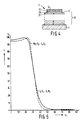
- Niobium pentoxide deposited in the whole temperature range from 80°C to 300°C has been found to have a high refractive index and when used with silicon dioxide the difference in refractive indices between them is large enough to get a sufficiently wide reflection band, that is a difference almost as large as that using titanium dioxide as shown in Figure 5.
- Figure 5 light incident on the filter at X L angles up to 32° is transmitted whereas light incident at greater angles is reflected, that is, its transmittance decreases to substantially zero.
- Factors which are considered to have contributed to the crazing include: (1) the fact that the substrates, that is the faceplates, have a large coefficient of expansion, that is one lying in the range 85 x 10 ⁇ 7 to 105 x 10 ⁇ 7 per degree C for temperatures between 0°C and 400°C in contrast to, in particular silicon dioxide which has a small coefficient of expansion. It is believed that niobium pentoxide enhances the overall elasticity of the multilayer filters to some extent thus reducing the crazing. (2) the fact that a large number of layers, typically of the order of 20 layers, have been used. Crazing is enhanced when the number of layers is increased and it is reduced when the number of layers is decreased.
- Nb2O5-SiO2 filters evaporated at substrate temperatures from 80°C to 300°C and Nb2O5-MgF2 filters evaporated at temperatures from 200°C and 300°C were annealed at 460°C substantially immediately after evaporation without any cooling-off of the substrate. This completely eliminated the occurrence of crazing for these filters.
- a suitable glass for a substrate for a cathode ray tube, in particular for projection television is a mixed-alkali glass free or almost free of lead oxide (PbO) and containing barium oxide (BaO) and strontium oxide (SrO) as the main X-ray absorbers.
- PbO lead oxide
- BaO barium oxide
- SrO strontium oxide
Landscapes
- Cathode-Ray Tubes And Fluorescent Screens For Display (AREA)
- Optical Filters (AREA)
- Manufacture Of Electron Tubes, Discharge Lamp Vessels, Lead-In Wires, And The Like (AREA)
- Formation Of Various Coating Films On Cathode Ray Tubes And Lamps (AREA)
- Vessels, Lead-In Wires, Accessory Apparatuses For Cathode-Ray Tubes (AREA)
- Video Image Reproduction Devices For Color Tv Systems (AREA)
Description
- The present invention relates to a method of manufacturing cathode ray tubes and to cathode ray tubes made by the method, the cathode ray tubes having a multilayer interference filter disposed between the cathodoluminescent display screen and the interior side of the faceplate. Such cathode ray tubes may compromise projection television tubes.
- A multilayer interference filter comprises a number of layers manufactured alternately from a material having a high refractive index and a material having a low refractive index. Projection display tubes including such multilayer interference filters are disclosed in EP-A-0170320, EP-A-0212715 and EP-A-0206381. Typically the alternate layers may comprise in the case of a low refractive index material SiO₂ (refractive index n = 1.47) or MgF₂ (n = 1.38) and in the case of a high refractive index material TiO₂ (n = 2.35) or Ta₂O₅ (n = 2.00) the precise value of n being dependent on the substrate temperature during evaporation and also on the annealing cycle after evaporation. These known multilayer filters comprise at least six but more typically at least fourteen layers alternately made from the respective high and low refractive index materials. The layers have an optical thickness nd , where n is the refractive index of the material of the layer and d is the thickness, the optical thickness nd of the individual layers being between 0.2λf and 0.3λf, where λf is equal to p x λ and λ is the desired central wavelength selected from the spectrum emitted by the luminescent material of the relevant display screen and p is a number between 1.18 and 1.32 for curved faceplates and between 1.18 and 1.36 for flat faceplates. The average optical thickness throughout the stack, excluding possible outer terminating 0.125 λf layers, is 0.25λf and λf is the central wavelength of the filter. Although these known shortwave pass multilayer interference filters perform reasonably satisfactorily further investigation has shown that the filters can suffer from crazing (formation of cracks) after the tube processing is completed. The crazing manifests itself, subsequent to the evaporation of the filter layers, after the tube processing which includes temperature cycles up to 400 to 460°C. Such crazing reduces the quality of the optical performance of the multilayer interference filter.
- An object of the present invention is to reduce and preferably avoid crazing in multilayer interference filters used in cathode ray tubes.
- Another object of the present invention is to reduce the cycle time for filter evaporation.
- According to a first aspect of the present invention there is provided a method of making a cathode ray tube having a cathodo luminescent screen and having a multilayer interference filter provided on an internally facing surface of a faceplate, the method including the step of depositing alternate layers of a material having a relatively high refractive index and a material having a relatively low refractive index on the faceplate, the material having a relatively high refractive index comprising niobium pentoxide.
- According to a second aspect of the present invention there is provided a cathode ray tube having a faceplate, a cathodoluminescent screen and a multilayer interference filter disposed between the faceplate and the screen, the filter comprising alternate layers of a material having a relatively high refractive index and a material having a relatively low refractive index deposited on the faceplate, wherein the material having a relatively high refractive index comprises niobium pentoxide.
- The advantages of using niobium pentoxide compared with titanium dioxide are firstly that it can be evaporated at a much lower temperature, 80°C for niobium pentoxide as compared to 300°C for titanium dioxide, which reduces the cycle time by about a factor of two, and secondly that the resulting filters with niobium pentoxide are more resistant to crazing when subjected to a heating cycle including temperatures up to 400 to 460°C, which heating cycle is necessary in processing the completed faceplate.
- When titanium dioxide is evaporated at lower temperatures the oxidation is slowed down appreciably, resulting in either not fully oxidized and therefore light absorbing layers or unacceptably long evaporation times and lower refractive indices of the layers. Niobium pentoxide can be evaporated with a high rate at 80°C already, yielding layers with a high refractive index. Such a high rate of evaporation of niobium pentoxide reduces at 80°C the cycle time for filter evaporation.
- The advantages of using niobium pentoxide compared with tantalum pentoxide are firstly that niobium pentoxide has a substantially higher refractive index yielding filters with a much broader reflection band and secondly that the interference filters with niobium pentoxide are more resistant to crazing when subjected to the heating cycle including temperatures of up to 400 to 460°C.
- One embodiment of a filter comprised niobium pentoxide as the high refractive index material and silicon dioxide as the low refractive index material. 20-layer Nb₂O₅/SiO₂ filters evaporated with substrate temperatures of 80, 200 and 300°C, had little or no crazing after being heated to temperatures of 460°C which in itself was an unexpected result. The reason for this surprise is that tests with: (1) 20 layer TiO₂/SiO₂ filters evaporated with substrate temperatures of 300 and 400°C, (2) 20 layer Ta₂O₅/SiO₂ filters evaporated with substrate temperatures of 80 and 200°C, and (3) (10/4)λf SiO₂ layers, that is layers having an equivalent thickness of SiO₂ as in the filters in (1) and (2) above, evaporated also with different substrate temperatures, all showed more and a mutually very similar amount of crazing when subjected to the same temperature cycling with temperatures of up to 460°C. Interleaving silicon dioxide with niobium pentoxide reduces the occurrence of crazing, in some cases even to such an extent that it no longer occurs. These comparative tests were performed using as substrate material, projection television faceplate glass having an expansion coefficient of 95 x 10⁻⁷.
- In another embodiment the filter comprised niobium pentoxide as the high refractive index material and magnesium fluoride as the low refractive index material. These 20-layer filters evaporated with substrate temperatures of 200 and 300°C did not shown any crazing.
- The cathode ray tube made in accordance with the present invention may comprise at least 9 layers, typically between 14 and 30 layers, each layer having an optical thickness nd, where n is the refractive index of the material, d is the thickness. The optical thickness nd is chosen to lie between 0.2λf and 0.3λf, more particularly between 0.23λf and 0.27λf, with an average optical thickness 0.25λf, where λf is equal to p × λ, where λ is the desired central wavelength selected from the spectrum emitted by the cathodoluminescent screen material and p is a number between 1.20 and 1.33.
- The faceplate may comprise a mixed-alkali glass substantially free of lead oxide having a coefficient of expansion in the range from 85 x 10⁻⁷ to 105 x 10⁻⁷ per degree C for temperatures between 0 and 400°C. The main components in weight percent of such a glass may be

with the restrictions that (1) BaO and SrO together lie between 16 and 24, and (2) the combination formed by Li₂O, Na₂O and K₂O lie between 14 and 17. - A letter entitled "Observation of exceptional temperature humidity stability in multilayer filter coatings" by Peter Martin, Walter Pawlewicz, David Coult and Joseph Jones published in Applied Optics
Vol 23 No. 9 1st May 1984 pages 1307 and 1308 discloses multilayer filter coatings made by refractive sputtering techniques using Si₃N₄/SiO₂ and Nb₂O₅/SiO₂ as the high and low refractive-index layers. The design of the Si₃N₄/SiO₂ filter was LL(HL)¹⁴HLL where L and H represent a quarterwave optical thickness of low- and high-refractive index material, respectively, whereas the design of the Nb₂O₅/SiO₂ filter was LL(HL)¹⁰LL. This letter reports that temperature and relative humidity testing with temperatures in the range 75°C to 140°C and relative humidities between 0 and 85% indicated that as far as transmittance in the sidebands is concerned, a Si₃N₄/SiO₂ coating was remarkably more stable than a Nb₂O₅/SiO₂ coating. This letter does not provide details of how each multilayer filter is made, especially the nature of the substrates, the deposition temperatures and subsequent processing of the filter all of which have some bearing on the crazing, the quality of bonding between, and the hardness of, the layers and the actual refractive indices of the material. Furthermore the authors of this letter have not addressed themselves to the provision of interference filters in cathode ray tubes where the problems are different because amongst other things: - 1. the much higher temperatures, above 400°C, used in tube processing. Crazing has been found to be initiated above about 330°C,
- 2. the electron bombardment during tube operation.
- The present invention also relates to a projection television system comprising three cathode ray tubes having cathodoluminescent screens luminescing in different colours, wherein at least one of said cathode ray tubes comprises a tube made in accordance with the present invention.
- The present invention will now be described, by way of example, with reference to the accompanying drawings, wherein:
- Figure 1 is a diagrammatic perspective view of a projection cathode ray tube with a portion of its envelope broken away,
- Figure 2 is a diagrammatic cross-section through a portion of a flat faceplate,
- Figure 3 is a diagrammatic cross-section through a curved faceplate of a display tube and inset is the portion of the faceplate shown enlarged,
- Figure 4 is a diagrammatic cross-section through a short wave pass multilayer interference filter, and
- Figure 5 shows the short wave pass characteristics of a known 20 layer TiO₂-SiO₂ filter (continuous line) including an 0.125λf terminating layer and of a 19 layer Nb₂O₅-SiO₂ filter (broken line) without a terminating layer; the ordinate representing transmittance and the abscissa the angle XL in degrees.
- In the drawings the same reference numerals have been used to indicate corresponding features.
- The projection
cathode ray tube 10 shown in Figure 1 comprises a glass envelope formed by afaceplate 12, acone 13 and aneck 14. Anelectron gun 15 is provided in theneck 14 and generates anelectron beam 16 which produces aspot 18 on acathodoluminescent screen structure 17 provided on thefaceplate 12. Thespot 18 is deflected in mutually perpendicular directions X and Y bydeflection coils 19 mounted at the neck-cone transition of the envelope. Electrical connections to the interior of the envelope are viapins 21 in acap 20. - The
tube 10 shown in Figure 1 has aflat faceplate 12 and a portion of thefaceplate 12 andscreen structure 17 are shown in Figure 2. Thescreen structure 17 comprises a multilayer short wavepass interference filter 22 applied to the interior surface of the faceplate, acathodoluminescent screen material 23 applied to thefilter 22 and analuminium film 24 covering thescreen material 23. The detailed construction of thefilter 22 will be described later with reference to Figure 4. - Figure 3 shows another embodiment of a faceplate of a projection television cathode ray tube in which at least the inside surface, but more conveniently both surfaces of the
faceplate 12, are convex as viewed from the interior of the envelope. The convex surfaces may be part-spherical having a radius of curvature between 150 mm and 730 mm. The angle of curvature φ, defined as the angle between the optical axis and a normal to the interior convex surface at a point furthest from the centre of the screen, has a maximum angle of 18°. Thestructure 17 of the screen, shown inset, is as described with reference to Figure 2. - Referring now to Figure 4, the
multilayer interference filter 22 comprises at least 9, but typically between 14 and 30, layers with alternate layers having (H) and low (L) refractive indices (n). The optical thickness of each of the layers is n.d, where n is the refractive index of the material and d the actual layer thickness, the optical thickness for the individual layers lies between 0.2λf and 0.3λf, more particularly between 0.23λf and 0.27λf with an average optical thickness throughout the stack of 0.25λf, where λf is equal to p x λ, p being a number between 1.20 and 1.33 and λ being the desired central wavelength selected from the spectrum emitted by thecathodoluminescent screen 23. In fabricating thefilter 22 the high refractive index layer 25 furthest from the faceplate has an optical thickness in the range specified but this layer 25 may be covered by a thinner, typically 0.125λf, terminatinglayer 26 having a lower (Lʹ) refractive index. - As is apparent from the foregoing description the value of the optical thickness is dependent on the value assigned p and λ. By way of example, when the screen material comprises a terbium activated substantially green luminescing phosphor having λ = 545 nm, p has a value between 1.20 and 1.26. A red phosphor material such as europium-activated yttrium oxide (Y₂O₃:Eu) has λ = 612 nm and p has a value between 1.20 and 1.26. Finally a blue phosphor material such as zinc sulphide-silver (ZnS:Ag) has λ = 460 nm and p has a value between 1.24 and 1.33.
- The optical thicknesses of a typical multilayer (HL)⁹H filter with an optional terminating layer is a shown in the following tabular summary:

- The
multilayer filter 22 is manufactured by depositing, for example by evaporation or sputtering, the high and low refractive index materials on a suitablyprepared faceplate 12 which acts as a substrate. In one example the high refractive index material is niobium pentoxide (Nb₂O₅) and the low refractive index material is silicon dioxide (SiO₂). In another example niobium pentoxide is used with magnesium fluoride (MgF₂) as the low refractive index material. Previously interference filters have been made using titanium pentoxide as the high refractive index material and silicon dioxide as the low refractive index material which have been evaporated onto a substrate at temperatures of the order of 300 to 400°C. Such filters although having good optical characteristics and bonding between adjacent layers were found to suffer from crazing after the subsequent tube processing steps including sedimentation of the phosphor material, lacquering, evaporation of the aluminium film over the phosphor/lacquer combination and heating to over 400°C to evaporate the lacquer and to get a good vacuum in the tube. Moreover, the cycle time required for the deposition is quite large due to the high substrate temperature needed for the evaporation of TiO₂. - The problem of crazing has been almost completely overcome by using niobium pentoxide evaporated preferably onto a cool substrate at typically 80°C, although higher temperature substrates can also be used. Niobium pentoxide deposited in the whole temperature range from 80°C to 300°C has been found to have a high refractive index and when used with silicon dioxide the difference in refractive indices between them is large enough to get a sufficiently wide reflection band, that is a difference almost as large as that using titanium dioxide as shown in Figure 5. In Figure 5 light incident on the filter at XL angles up to 32° is transmitted whereas light incident at greater angles is reflected, that is, its transmittance decreases to substantially zero. In consequence a bright substantially haze-free image is obtained, with an improved luminosity (by typically a factor of 1.5 to 1.9), a more saturated colour (particularly cathode ray tubes provided with green terbium activated phosphors and with a blue zinc sulphide-silver phosphor) leading to substantially less chromatic aberration when used in a projection television system, and improved contrast.
- In the case of using magnesium fluoride as the low refractive index material it is necessary to do the evaporation of niobium pentoxide and magnesium fluoride at temperatures of the order of 200°C to 300°C to ensure that the layers have the required degree of hardness and bond well to each other and to the substrate. When using 300°C, the hardness of the layers is greater than when using 200°C.
- Factors which are considered to have contributed to the crazing include: (1) the fact that the substrates, that is the faceplates, have a large coefficient of expansion, that is one lying in the range 85 x 10⁻⁷ to 105 x 10⁻⁷ per degree C for temperatures between 0°C and 400°C in contrast to, in particular silicon dioxide which has a small coefficient of expansion. It is believed that niobium pentoxide enhances the overall elasticity of the multilayer filters to some extent thus reducing the crazing. (2) the fact that a large number of layers, typically of the order of 20 layers, have been used. Crazing is enhanced when the number of layers is increased and it is reduced when the number of layers is decreased. (3) the fact that the filters have usually been annealed some time (one or more days) after evaporation. Allowing the substrate to cool to ambient temperature before annealing and thus allowing the water vapour to penetrate into the pores of the filter has been found to encourage crazing. In recent experiments Nb₂O₅-SiO₂ filters evaporated at substrate temperatures from 80°C to 300°C and Nb₂O₅-MgF₂ filters evaporated at temperatures from 200°C and 300°C were annealed at 460°C substantially immediately after evaporation without any cooling-off of the substrate. This completely eliminated the occurrence of crazing for these filters.
- A suitable glass for a substrate for a cathode ray tube, in particular for projection television is a mixed-alkali glass free or almost free of lead oxide (PbO) and containing barium oxide (BaO) and strontium oxide (SrO) as the main X-ray absorbers.
The compositions in weight per cent of suitable existing glasses to use as substrates are as follows:
Claims (30)
- A method of making a cathode ray tube having a cathodo luminescent screen and having a multilayer interference filter provided on an internally facing surface of a faceplate, the method including the step of depositing alternate layers of a material having a relatively high refractive index and a material having a relatively low refractive index on the faceplate, the material having a relatively high refractive index comprising niobium pentoxide.
- A method as claimed in claim 1, characterised in that at least 9 alternate layers are deposited, the layers having an optical thickness nd, where n is the refractive index of the materials and d is the thickness, the optical thickness nd of the individual layers being between 0.2λf and 0.3λf, with an average optical thickness of the layers being 0.25λf, where λf is equal to p x λ, where λ is the desired central wavelength selected from the spectrum emitted by the cathodoluminescent screen material and p is a number between 1.20 and 1.33.
- A method as claimed in claim 1 or 2, characterised in that the low refractive index material comprises silicon dioxide, and the alternate layers are deposited at a temperature in the range of substantially 80°C to substantially 300°C.
- A method as claimed in claim 1 or 2, characterised in that the low refractive index material comprises magnesium fluoride, and the alternate layers are deposited at a temperature in the range of substantially 200°C to substantially 300°C.
- A method as claimed in any one of claims 1 to 4, characterised in that the multilayer interference filter is annealed whilst the faceplate is still at above ambient temperature.
- A method as claimed in any one of claims 1 to 5, characterised in that the faceplate comprises a mixed-alkali glass substantially free of lead oxide (PbO).
- A method as claimed in claim 6, characterised in that the faceplate has a coefficient of expansion in the range 85 x 10⁻⁷ to 105 x 10⁻⁷ per degree centigrade for temperatures between 0 and 400°C.
- A method as claimed in claim 6 or 7, characterised in that the glass composition in weight per cent comprises as main components:with the restrictions that (1) BaO and SrO together lie between 16 to 24, and (2) the combination formed by Li₂O, Na₂O and K₂O lie between 14 and 17.

- A method as claimed in any one of claims 1 to 8, characterised in that a cathodoluminescent screen is provided on the interference filter.
- A method as claimed in claim 2 or any one of claims 3 to 8 when appended to claim 2, characterised in that the last layer of average optical thickness of 0.25λf of the filter comprises a material having a high refractive index, a terminating layer is provided on the last layer, the terminating layer having a lower refractive index than the last layer and a thickness of substantially less than an average optical thickness of 0.25λf and in which a cathodoluminescent screen is provided on the terminating layer.
- A cathode ray tube having a faceplate, a cathodoluminescent screen and a multilayer interference filter disposed between the faceplate and the screen, the filter comprising alternate layers of a material having a relatively high refractive index and a material having a relatively low refractive index deposited on the faceplate, wherein the material having a relatively high refractive index comprises niobium pentoxide.
- A tube as claimed in claim 11, characterised in that the filter comprises at least 9 layers, the layers having an optical thickness nd, where n is the refractive index of the materials and d is the thickness, the optical thickness nd of the individual layers being between 0.2λf and 0.3λf, with an average optical thickness of the layers being 0.25λf, where λf is equal to p x λ, where λ is the desired central wavelength selected from the spectrum emitted by the cathodoluminescent screen material and p is a number between 1.20 and 1.33.
- A tube as claimed in claim 12, characterised in that the filter has between 14 to 30 layers.
- A tube as claimed in claim 12 or 13, characterised in that nd is between 0.23λf and 0.27λf.
- A tube as claimed in any one of claims 11 to 14, characterised in that the low refractive index material comprises silicon dioxide.
- A tube as claimed in any one of claims 11 to 14, characterised in that the low refractive index material comprises magnesium fluoride.
- A tube as claimed in any one of claims 11 to 16, characterised in that the filter has been annealed substantially immediately after the layers have been deposited.
- A tube as claimed in any one of claims 11 to 17, characterised in that the faceplate comprises a mixed-alkali glass substantially free of lead oxide (PbO).
- A tube as claimed in claim 18, characterised in that the faceplate has a coefficient of expansion in the range 85 x 10⁻⁷ to 105 x 10⁻⁷ per degree centigrade for temperatures between 0 and 400°C.
- A tube as claimed in claim 18 or 19, characterised in that the glass composition in weight per cent comprises as main components:with the restrictions that (1) BaO and SrO together lie between 16 to 24, and (2) the combination formed by Li₂O, Na₂O and K₂O lie between 14 and 17.

- A tube as claimed in any one of claims 11 to 20, characterised in that the inside of the faceplate is convex with a maximum angle of curvature φ = 18°, where φ is the angle between the optical axis and a normal to the convex surface at a point furthest from the centre of the screen.
- A tube as claimed in claim 21, characterised in that the convex faceplate is substantially spherical and has a radius of curvature between 150 mm and 730 mm.
- A tube as claimed in claim 15 or 16, characterised in that the cathodoluminescent screen comprises a terbium activated substantially green luminescing phosphor having λ = 545 nm and p is a number between 1.20 and 1.26.
- A tube as claimed in claim 15 or 16, characterised in that the cathodoluminescent screen comprises a europium-activated yttrium oxide phosphor (Y₂O₃:Eu) having λ = 612 nm and p is a number between 1.20 and 1.26.
- A tube as claimed in claim 15 or 16, characterised in that the cathodoluminescent screen comprises a zinc sulphide-silver (ZnS:Ag) having λ = 460 nm and p is a number between 1.24 and 1.33.
- A tube as claimed in claim 12 or any one of claims 13 to 25, when appended to claim 12, characterised in that the average optical thickness of the layers is 0.25λf, the layer furthest from the faceplate having a thickness of substantially 0.25λf comprises a material having a high refractive index, and in that the layer furthest from the faceplate is covered by the cathodoluminescent material.
- A tube as claimed in claim 26, characterised in that a terminating layer is disposed between the layer of high refractive index material furthest from the faceplate and the layer of cathodoluminescent screen material, the terminating layer having an optical thickness of substantially 0.125λf and being of a material having a lower refractive index than that of the adjacent filter layer.
- A projection television system comprising three cathode ray tubes having cathodoluminescent screens luminescing in different colours, characterised in that at least one of said cathode ray tubes is a cathode ray tube as claimed in claim 23.
- A projection television system comprising three cathode ray tubes having cathodoluminescent screens luminescing in different colours, characterised in that at least one of said cathode ray tubes is a cathode ray tube as claimed in claim 24.
- A projection television system comprising three cathode ray tubes having cathodoluminescent screens luminescing in different colours, characterised in that at least one of said cathode ray tubes is a cathode ray tube as claimed in claim 25.
Applications Claiming Priority (2)
| Application Number | Priority Date | Filing Date | Title |
|---|---|---|---|
| GB8612358 | 1986-05-21 | ||
| GB868612358A GB8612358D0 (en) | 1986-05-21 | 1986-05-21 | Cathode ray tube |
Publications (3)
| Publication Number | Publication Date |
|---|---|
| EP0246696A2 EP0246696A2 (en) | 1987-11-25 |
| EP0246696A3 EP0246696A3 (en) | 1990-04-18 |
| EP0246696B1 true EP0246696B1 (en) | 1994-03-30 |
Family
ID=10598202
Family Applications (1)
| Application Number | Title | Priority Date | Filing Date |
|---|---|---|---|
| EP87200874A Expired - Lifetime EP0246696B1 (en) | 1986-05-21 | 1987-05-12 | A method of manufacturing a cathode ray tube and a cathode ray tube made by the method |
Country Status (5)
| Country | Link |
|---|---|
| US (1) | US5068568A (en) |
| EP (1) | EP0246696B1 (en) |
| JP (1) | JPH07101600B2 (en) |
| DE (1) | DE3789468T2 (en) |
| GB (1) | GB8612358D0 (en) |
Families Citing this family (21)
| Publication number | Priority date | Publication date | Assignee | Title |
|---|---|---|---|---|
| GB8707975D0 (en) * | 1987-04-03 | 1987-05-07 | Philips Nv | Colour cathode ray tube |
| JPH0218841A (en) * | 1988-07-06 | 1990-01-23 | Mitsubishi Electric Corp | Cathode-ray tube |
| US4937661A (en) * | 1988-07-11 | 1990-06-26 | North American Philips Corporation | Projection television display tube and device having band pass interference filter |
| US5209690A (en) * | 1988-09-08 | 1993-05-11 | U.S. Philips Corporation | Method of vapor depositing an interference filter layer on the inside of a display window, a display window, a projection cathode ray tube and a projection television apparatus |
| NL8802210A (en) * | 1988-09-08 | 1990-04-02 | Koninkl Philips Electronics Nv | METHOD FOR VAPORATING AN INTERFERENCE FILTER COATING ON THE INSIDE OF AN IMAGE WINDOW, AN IMAGE WINDOW, A PROJECTION CATHODIC TUBE AND A PROJECTION TELEVISION DEVICE. |
| FR2640425A1 (en) * | 1988-12-09 | 1990-06-15 | Malifaud Pierre | Process for the spectral selection of radiation and device for implementation, especially video image television projector |
| FR2642897A1 (en) * | 1989-02-03 | 1990-08-10 | Thomson Csf | Fluorescent screen for cathode-ray tube |
| US5179318A (en) * | 1989-07-05 | 1993-01-12 | Nippon Sheet Glass Co., Ltd. | Cathode-ray tube with interference filter |
| JP2512204B2 (en) * | 1990-05-09 | 1996-07-03 | 三菱電機株式会社 | Projection type cathode ray tube |
| US5243255A (en) * | 1990-10-24 | 1993-09-07 | Mitsubishi Denki Kabushiki Kaisha | Cathode-ray tube with low reflectivity film |
| KR950014541B1 (en) * | 1991-05-24 | 1995-12-05 | 미쯔비시덴끼 가부시끼가이샤 | Cpt having intermediate layer |
| US5828493A (en) * | 1992-07-24 | 1998-10-27 | Dielectric Coating Industries | Reflectors |
| JP2981528B2 (en) * | 1992-12-25 | 1999-11-22 | 三菱電機株式会社 | Cathode ray tube and method of manufacturing the same |
| US6074789A (en) * | 1994-03-08 | 2000-06-13 | Philips Electronics N.A. Corp. | Method for producing phosphor screens, and color cathode ray tubes incorporating same |
| JP3368110B2 (en) | 1995-08-01 | 2003-01-20 | キヤノン株式会社 | Light source device and optical equipment |
| KR100453188B1 (en) | 1999-05-31 | 2004-10-15 | 삼성에스디아이 주식회사 | Cathode layer tube improved in contrast and method for producing the same |
| KR100615154B1 (en) | 1999-08-19 | 2006-08-25 | 삼성에스디아이 주식회사 | Cathode layer tube improved in contrast |
| JP4345158B2 (en) * | 1999-10-15 | 2009-10-14 | ソニー株式会社 | Optical component manufacturing apparatus and manufacturing method |
| JP2002075227A (en) * | 2000-06-14 | 2002-03-15 | Sharp Corp | Gas discharge display device, plasma address liquid crystal display device and manufacturing method for the same |
| KR100786854B1 (en) * | 2001-02-06 | 2007-12-20 | 삼성에스디아이 주식회사 | A filter for a display, a method for preparing the same and a display comprising the same |
| US7019452B2 (en) * | 2003-05-29 | 2006-03-28 | General Electric Company | Boron-containing red light-emitting phosphors and light sources incorporating the same |
Family Cites Families (7)
| Publication number | Priority date | Publication date | Assignee | Title |
|---|---|---|---|---|
| US4065697A (en) * | 1969-02-17 | 1977-12-27 | Owens-Illinois, Inc. | Cathode-ray tube |
| NL6907310A (en) * | 1969-05-13 | 1970-11-17 | ||
| US3805107A (en) * | 1972-02-17 | 1974-04-16 | Corning Glass Works | Faceplate for television picture tube |
| US4310783A (en) * | 1979-05-07 | 1982-01-12 | Temple Michael D | Cathode ray tube face plate construction for suppressing the halo having a low reflection and method |
| NL8301824A (en) * | 1983-05-24 | 1984-12-17 | Philips Nv | OPTICAL ELEMENT COMPRISING A TRANSPARENT SUBSTRATE AND ANTI-REFLECTIVE CLOTHING FOR THE WAVE LENGTH AREA IN THE NEAR INFRARED. |
| NL8402304A (en) * | 1984-07-20 | 1986-02-17 | Philips Nv | PICTURE TUBE. |
| GB2176048B (en) * | 1985-05-29 | 1989-07-05 | Philips Nv | Projection television display tube and projection television device comprising at least one such tube |
-
1986
- 1986-05-21 GB GB868612358A patent/GB8612358D0/en active Pending
-
1987
- 1987-05-12 DE DE3789468T patent/DE3789468T2/en not_active Expired - Fee Related
- 1987-05-12 EP EP87200874A patent/EP0246696B1/en not_active Expired - Lifetime
- 1987-05-21 JP JP62122674A patent/JPH07101600B2/en not_active Expired - Lifetime
-
1990
- 1990-05-15 US US07/524,718 patent/US5068568A/en not_active Expired - Fee Related
Also Published As
| Publication number | Publication date |
|---|---|
| GB8612358D0 (en) | 1986-06-25 |
| DE3789468D1 (en) | 1994-05-05 |
| JPH07101600B2 (en) | 1995-11-01 |
| JPS62283535A (en) | 1987-12-09 |
| EP0246696A2 (en) | 1987-11-25 |
| US5068568A (en) | 1991-11-26 |
| DE3789468T2 (en) | 1994-10-20 |
| EP0246696A3 (en) | 1990-04-18 |
Similar Documents
| Publication | Publication Date | Title |
|---|---|---|
| EP0246696B1 (en) | A method of manufacturing a cathode ray tube and a cathode ray tube made by the method | |
| EP0170320B1 (en) | Display tube | |
| EP0206381B1 (en) | Projection television display tube and projection television device comprising at least one such tube | |
| US4798994A (en) | Low reflectance display device | |
| US5599579A (en) | Cathode-ray tube with anti-reflective coating | |
| EP0335680A2 (en) | A cathode ray tube | |
| US20050242725A1 (en) | Glass composition and paste composition suitable for a plasma display panel, and plasma display panel | |
| US4707635A (en) | Cathode ray tube having a fluorescent layer with varying amounts of silica | |
| US4977347A (en) | Color filter and cathode-ray tube using the color filter | |
| US6479928B1 (en) | Cathode ray tube | |
| US4684846A (en) | Luminescent screen having restored cavities and display tube having such a screen | |
| JP2000206307A (en) | Functional film and cathode-ray tube adopting it | |
| EP0925598B1 (en) | Color display device having color filter layers | |
| JP2001226147A (en) | Electrically conductive antireflection film and glass panel for cathode ray tube on which the film is deposited | |
| CN1307354A (en) | Colour picture tube | |
| JPH11283529A (en) | Cathode-ray tube and its manufacture | |
| JPH10302683A (en) | Light emitting display device | |
| JP2001126646A (en) | Cathode-ray tube | |
| JPH02160342A (en) | Image tube | |
| JPH03159034A (en) | Cathode-ray tube faceplate | |
| JPS587749A (en) | Color crt | |
| JPH03241642A (en) | Cathode-ray tube faceplate | |
| JP2002100309A (en) | Cathode-ray tube | |
| JP2001110342A (en) | Cathode ray tube |
Legal Events
| Date | Code | Title | Description |
|---|---|---|---|
| PUAI | Public reference made under article 153(3) epc to a published international application that has entered the european phase |
Free format text: ORIGINAL CODE: 0009012 |
|
| AK | Designated contracting states |
Kind code of ref document: A2 Designated state(s): DE FR GB NL |
|
| PUAL | Search report despatched |
Free format text: ORIGINAL CODE: 0009013 |
|
| AK | Designated contracting states |
Kind code of ref document: A3 Designated state(s): DE FR GB NL |
|
| 17P | Request for examination filed |
Effective date: 19901016 |
|
| 17Q | First examination report despatched |
Effective date: 19921124 |
|
| GRAA | (expected) grant |
Free format text: ORIGINAL CODE: 0009210 |
|
| AK | Designated contracting states |
Kind code of ref document: B1 Designated state(s): DE FR GB NL |
|
| PG25 | Lapsed in a contracting state [announced via postgrant information from national office to epo] |
Ref country code: NL Effective date: 19940330 |
|
| REF | Corresponds to: |
Ref document number: 3789468 Country of ref document: DE Date of ref document: 19940505 |
|
| ET | Fr: translation filed | ||
| NLV1 | Nl: lapsed or annulled due to failure to fulfill the requirements of art. 29p and 29m of the patents act | ||
| PLBE | No opposition filed within time limit |
Free format text: ORIGINAL CODE: 0009261 |
|
| STAA | Information on the status of an ep patent application or granted ep patent |
Free format text: STATUS: NO OPPOSITION FILED WITHIN TIME LIMIT |
|
| 26N | No opposition filed | ||
| REG | Reference to a national code |
Ref country code: FR Ref legal event code: CD |
|
| PGFP | Annual fee paid to national office [announced via postgrant information from national office to epo] |
Ref country code: GB Payment date: 19960430 Year of fee payment: 10 |
|
| PGFP | Annual fee paid to national office [announced via postgrant information from national office to epo] |
Ref country code: FR Payment date: 19960530 Year of fee payment: 10 |
|
| PGFP | Annual fee paid to national office [announced via postgrant information from national office to epo] |
Ref country code: DE Payment date: 19960724 Year of fee payment: 10 |
|
| PG25 | Lapsed in a contracting state [announced via postgrant information from national office to epo] |
Ref country code: GB Effective date: 19970512 |
|
| GBPC | Gb: european patent ceased through non-payment of renewal fee |
Effective date: 19970512 |
|
| PG25 | Lapsed in a contracting state [announced via postgrant information from national office to epo] |
Ref country code: FR Free format text: LAPSE BECAUSE OF NON-PAYMENT OF DUE FEES Effective date: 19980130 |
|
| PG25 | Lapsed in a contracting state [announced via postgrant information from national office to epo] |
Ref country code: DE Free format text: LAPSE BECAUSE OF NON-PAYMENT OF DUE FEES Effective date: 19980203 |
|
| REG | Reference to a national code |
Ref country code: FR Ref legal event code: ST |