EP0245903A1 - Discrete cosine transform arrangement - Google Patents
Discrete cosine transform arrangement Download PDFInfo
- Publication number
- EP0245903A1 EP0245903A1 EP87200830A EP87200830A EP0245903A1 EP 0245903 A1 EP0245903 A1 EP 0245903A1 EP 87200830 A EP87200830 A EP 87200830A EP 87200830 A EP87200830 A EP 87200830A EP 0245903 A1 EP0245903 A1 EP 0245903A1
- Authority
- EP
- European Patent Office
- Prior art keywords
- samples
- sum
- arrangement
- auxiliary
- difference
- Prior art date
- Legal status (The legal status is an assumption and is not a legal conclusion. Google has not performed a legal analysis and makes no representation as to the accuracy of the status listed.)
- Withdrawn
Links
- 238000004364 calculation method Methods 0.000 claims abstract description 6
- 230000015654 memory Effects 0.000 claims description 34
- 238000012546 transfer Methods 0.000 claims description 18
- 230000009466 transformation Effects 0.000 claims description 15
- 238000009825 accumulation Methods 0.000 claims description 5
- 239000011159 matrix material Substances 0.000 description 30
- 230000004044 response Effects 0.000 description 15
- 238000000034 method Methods 0.000 description 8
- 238000007792 addition Methods 0.000 description 6
- 238000004422 calculation algorithm Methods 0.000 description 6
- 238000005070 sampling Methods 0.000 description 6
- 238000010586 diagram Methods 0.000 description 4
- 238000012545 processing Methods 0.000 description 3
- 230000009467 reduction Effects 0.000 description 2
- 230000002596 correlated effect Effects 0.000 description 1
- 230000000875 corresponding effect Effects 0.000 description 1
- 230000002349 favourable effect Effects 0.000 description 1
- 230000006870 function Effects 0.000 description 1
- 238000005192 partition Methods 0.000 description 1
- 230000008569 process Effects 0.000 description 1
- 238000012552 review Methods 0.000 description 1
Images


Classifications
-
- H—ELECTRICITY
- H04—ELECTRIC COMMUNICATION TECHNIQUE
- H04N—PICTORIAL COMMUNICATION, e.g. TELEVISION
- H04N11/00—Colour television systems
- H04N11/04—Colour television systems using pulse code modulation
-
- G—PHYSICS
- G06—COMPUTING; CALCULATING OR COUNTING
- G06F—ELECTRIC DIGITAL DATA PROCESSING
- G06F17/00—Digital computing or data processing equipment or methods, specially adapted for specific functions
- G06F17/10—Complex mathematical operations
- G06F17/14—Fourier, Walsh or analogous domain transformations, e.g. Laplace, Hilbert, Karhunen-Loeve, transforms
- G06F17/147—Discrete orthonormal transforms, e.g. discrete cosine transform, discrete sine transform, and variations therefrom, e.g. modified discrete cosine transform, integer transforms approximating the discrete cosine transform
Definitions
- the invention relates to an arrangement for real-time calculation of the discrete cosine transformation coefficients of a group of N input samples of a digital input signal. It is particularly intended for performing a transform coding of a digitalised video signal to reduce its bit rate. Such an arrangement will hereinafter be referred to as a DCT arrangement.
- the invention also relates to an arrangement for calculating the original N input samples from the coefficients thus obtained.
- Such an arrangement will be referred to as an IDCT arrangement.
- NxN mutually orthogonal basic pictures
- the block of NxN picture elements will be represented by an NxN matrix X
- the weighting factors will be arranged in an NxN matrix Y
- an NxN transform matrix A will be defined which is related to the set of basic pictures B(i, k). More particularly there applies that :
- A represents a matrix in which each column is equal to the i-th column of the transform matrix A and A T k represents a matrix each row of which is equal to the k-th row of the matrix A.
- AT represents the transposed matrix of A.
- the number of non-negligible weighting factors appearing from such a transformation is found to be closely related to the structure of the basic pictures chosen and hence to the transform matrix chosen.
- the most optimum transform matrix which is nowadays frequently used is the discrete cosine transform matrix whose elements a(i,k) are defined as follows.
- Q is a scaling constant which is equal to 2/N if this matrix is used to calculate the weighting factors for the direct transformation and which is equalto 1 if it is used for the inverse transformation.
- N multiplications must be performed for each N product element of the product matrix and N(N-1) additions are required.
- a DCT arrangement whose implementation is based on this direct method is described, for example, in Reference 3.
- the drawback of these known methods is that the intermediate results occurring during the calculation process must be very accurate due to subsequent further processing steps to be performed (this means that the word length of these intermediate results must be large). These further processing steps are notably multiplications.
- the invention has for its object to provide an alternative embodiment of a DCT arrangement in which considerably less stringent requirements need to be imposed on the accuracy of the intermediate results, possibly in exchange for an acceptable increase of the number of mathematical operations to be performed as compared with the DCT arrangement which is described in Reference 5.
- a DCT arrangement comprises:
- each incoming picture element is multiplied only once by some number, in this case the multiplication factor of the transform matrix, so that the accuracy of the intermediate results need to be no greater than the accuracy with which the coefficients are desired.
- this is accompanied by an increase of the number of mathematical operations to be performed (at least compared with the DCT arrangement described in Reference 5).
- a transform arrangement 5 which receives the video signal samples x(q) and converts them into transform weighting factors y(m). These are subsequently applied to a variable word length encoder 6 which converts each transform weighting factor into a code word z(m) of suitable word length. It comprises an auxiliary encoder 61 which receives the transform weighting factors and ensures the actual encoding. The word length of the code word z(m) is determined by a quantity b(j) which is supplied by a bit assignment memory 62. This auxiliary encoder thus supplies code words z(m) varying in length and also ensures that given transform weighting factors y(m) are ignored in that no bit is made available for their encoding.
- Reference 6 A particularly favourable embodiment of the encoder 6 is described in Reference 6. It is to be noted that the samples taken from a video signal and hence from a video picture are shown diagrammatically by means of dots in Figure 2.
- R is the number of video signal samples of a television line.
- the input 70 of this block-forming circuit 7 and the outputs of each delay line 71 (.) are connected via AND-gate circuits 72(.) to inputs of an OR-gate circuit 73.
- Each AND-gate circuit also receives 8 control pulses in such a manner that first 8 video signal samples are applied from the delay line 71(7) to the transform circuit, then 8 video signal samples from the delay line 71(6), then 8 video signal samples from the delay line 71 (5), and so forth.
- These control pulses are generated by a modulo 64 counter 74 to which the sampling pulses are applied.
- a decoding network 75 having eight outputs 75 (.) which are connected to inputs of the AND-gate circuits is connected to this counter 74.
- This decoding network supplies a logic !'1" at the output 75(7) each time the counter has one of the counting positions 1,2,3,...8.
- a logic "1" occurs at the output 75(6) each time the counter has one of the counting positions 9, 10, 11, ... 16 and so forth. In this manner the video signals of a block occur successively and row by row at the output of the OR-gate circuit 73.
- the transform circuit 8 is constituted by a first transformer 9, a memory 10 and a second transformer 11. These transformers have the same structure and are each constituted by a DCT arrangement.
- this DCT matrix has a very specific structure due to the periodical character of the goniometric function.
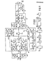
- FIG. 7 An embodiment of the DCT arrangement whose implementation is based on the new DCT algorithm shown in Figure 6 is shown in Figure 7. It comprises a shuffle circuit 903 to which the video signal samples are applied in the sequence x i,0 , x i,2' ... x i,7 . It supplies the same video signal samples but in a different sequence, more specifically as follows x i,0 , x i,7 x i,3 , x i,4 , x i,1 , x i,6 , x i,2 , x i,5 . In this sequence they are applied via an input 901 to a combination circuit 90. Auxiliary samples are also applied thereto via an input 902.
- Addition and subtraction operations are performed on these video signal samples and auxiliary samples so that the sum and difference samples denoted by u 0 to u 7 inclusive in Figure 6 and bracketed in Figure 5 are obtained.
- These samples are applied to a selection circuit 91 which applies the sum samples u 0 , u 1 , u 2 , u 3 , v 0 , v 1 shown in Figure 6 as auxiliary samples to the input 902 of the combination circuit 90.
- the difference samples u 4 , u 5 , u 6 , u 7 , v 2 , v 3 , w 1 as well as the sum sample w 0 are applied as transfer samples to a multiplier circuit.92 in which these transfer samples are multiplied by the associated transform elements shown in Figure 6.
- the product samples z 0 to z 21 inclusive shown in Figure 6 are thereby obtained. These are applied to an accumulator circuit 93 which, as is shown in Figure 6, adds given product samples together to obtain the desired coefficients p i,m . These coefficients may be stored temporarily in a buffer memory 94.
- a memory circuit 95 as a buffer circuit is incorporated for practical reasons between the selection circuit 91 and the multiplier circuit 92. This has been done because the rate at which mathematical operations must be performed inthe combination circuit 90 can be lower than the rate at which mathematical operations must be performed in the multiplier circuit 92.
- Figure 8 shows a more detailed embodiment of the DCT arrangement.
- the operation of this arrangement is diagrammatically shown in Figure 10. More particularly the first column in Figure 10 indicates the reference numbers of a number of memories present in Figure 8 and the other columns represent the contents of these memories after a clock pulse has occurred. These clock pulses are enumerated 1 to 53, inclusive in the first row.
- the indices i as used in the foregoing as well as in figure 6 have been omitted for the video signal samples and for the coefficients. It is to be noted that in this Figure 10 a dash "-" means that the content of the relevant memory is unchanged.
- the shuffle circuit 903 is constituted by two memories 903 (.) with addressable memory locations ; for example, RAMs. Each of them receives the video signal samples x i,k ⁇
- These memories are controlled by write and read address commands WR j and R j in such a manner that the presented video signal samples are written into one of them, while simultaneously the video signal samples present in the other memory are read therefrom.
- the video signal samples x i,0' x i,3' x i,1 , x i,2 read from this memory in response to one of the clock pulses 1, 7, 13, 19 shown in Figure 10 are temporarily stored in the combination circuit 90 in a buffer memory 904(1) which may be formed as a latch and is controlled by a latch enable command LE 1 ,
- the video signal samples x i,7 , x i,4 , x i,6 , x i,5 read from this memory 903(.) in response to one of the clock pulses 4, 10, 16, 22 are applied in the combination circuit 90 to latch 904(2) which is controlled by latch enable command LE 2 .
- the actual contents of the two latches 904(.) are applied in response to each further clock pulse 6, 12, 18, 24, 30, 36, 45 via selection circuits 905(.) to latches 906(.) which take over these actual contents in response to the occurrence of the latch enable command LE 3 .
- the selection circuits 905(.) are built up in the same manner and each have two inputs 9051(.) and 9052(.)
- the inputs 9052(.) receive the video signal sample which is stored in latch 904(.) and the inputs 9051(.) receive auxiliary samples which are applied via inputs 902(.) to the combination circuit.
- These selection circuits 905(.) also receive two control commands SEL 1 and SEL 2 which ensure that either the video signal sample from latch 904(.) or the auxiliary sample at input 9051(.) is stored in latch 906(.).
- this selection circuit may be simply formed by two AND-gate circuits 9O53(.) and 9054(.) and an OR-gate circuit 9055 (.).
- latches 906(.) comprise the video signal samples x i,0 and x i 7 , whilst these latches comprise the auxiliary samples u 1 and u 2 after the occurrence of, for example, clock pulse 36.
- the samples present in the latches 906(.) are applied to an adder-subtractor circuit 907 which is controlled by an adding command AC and a subtraction command SC.
- This circuit subtracts each time the two samples present in the latches 906(1) and 906(2) so that the difference samples u 7 , u 4 , u 6 , u 5' v 3' v 2' w 1 are obtained. They are also added together so that the sum samples u 0' u 3' u 1 , u 2 , v 0 , v 1' w 0 are obtained.
- Each sample is applied to the selection circuit 91 where such a sample, in response to the occurrence of a latch enable command LE4 (coinciding with the clock pulses 3, 9, 12, 15, 18, 21, 24, 27, 30, 33, 36, 39, 42, 28, 51) is taken up in a latch 910.
- Each difference sample and the sum sample w 0 is subsequently applied directly as a transfer sample to the buffer circuit 95.
- the other sum samples are temporarily stored in one of the three latches 911(.) which are controlled by the latch enable commands LES 5 , LE 6 and LE 7 , respectively.
- Figure 10 shows in detail which sum sample is stored in which latch.
- the sum sample u 0 supplied in response to the two sum samples u 0 and u 3 by the adder-subtractar circuit is stored in latch 910 in response to clock pulse 36 and is subsequently stored in latch 911(1) in response to clock pulse 37, and so forth, As is apparent from Figure 10, all eight video signal samples x i,0 to x i,7 inclusive are converted after 52 clock pulses into the eight transfer samples u 4 , u 5 , u 6 , u 7 , v 2 , v 3 , v 0' w 1 which are all present in the store 951(1) at that instant.
- the buffer circuit 95 is built up in the same manner as the shuffle circuit 903. It also comprises two RAM's 951(.) which are controlled by the read and write address commands R and WR j , respectively. Also in this case the control is such that all transfer samples which are calculated, starting from a given group of video signal samples x i,k which are present in one of the memories 9031(.), are written into one of the memories 951 (.).
- the actually calculated transfer samples are written into memory 951(1) and that the memory 951(2) comprises all transfer samples which are calculated in the previous cycle of 52 clock pulses. As is shown in Figure 10 this means that after the fourth clock pulse the memory 951(2) comprises a completely new set of transfer samples.
- these transfer samples are also applied to the multiplier circuit 92.
- This circuit comprises two further latches 921 and 922 which are controlled by latch enable commands LE 8 and LE 9 , respectively.
- a multiplier 923 which receives the transform elements C m from a memory 924, for example, a ROM is incorporated between the two latches. This ROM is controlled by an address command R 5 .
- the content of latch 922 is applied to the accumulator circuit 93 which is built up in known manner and comprises an adder circuit 931 and a memory 932.
- This memory which can only comprise one word supplied by the adder 931, is reset by means of a reset command RES.
- the sum number supplied by the adder 931 is written into this memory in response to a write command WR 5 . This sum number may also be written into the buffer memory 94 by means of a further write command BE.
- the transfer samples u7, u 4 , u 6 , u 5 are written into the latch 921 in response to the clock pulses 6, 8, 10 and 12, respectively, multiplied by the transform elements C 1 16 , C 7 16 , C 3 16' C 5 16' respectively, so that the product samples Z 18, z 6 ,z 14 and z 10 are successively obtained which are accumulated in the accumulator circuit 93 so that the transform coefficient P i,1 can be written into the buffer memory 94 in response to clock pulse 16.
- the other transform coefficients are obtained so that this buffer memory 94, in response to clock pulse 52, comprises a completely new set of eight transform coefficients.
- the same situation occurred at the instant after the occurrence of the fourth clock pulse.
- the above-mentioned clock pulses occur at a rate which is, for example, six times as high as the sampling frequency f s at which the video signal samples occur.
- a frequency multiplier circuit 96 they are derived from the sampling pulses S(qT) which are supplied by a pulse source 97.
- These clock pulses are also used to generate the various commands. They are therefore applied to a modulo-48 counter 98 whose counting position is applied as an address to a memory 99 with addressable memory locations; for example, a ROM. Each memory location comprises the values "0" and "1" of all commands. These commands are applied to the different elements by means of a bus 100 consisting of many lines.
- an inverse transformation is to be performed on the ultimately obtained weighting factors in order to recover the original picture elements.
- This inverse transformation requires an inverse discrete cosine transformation. It can be realized by means of the IDCT arrangement shown in Figure 11. It differs from the DCT arrangement of Figure 7 exclusively in the location of the circuit combinations 90, 91 and 92, 93.
Abstract
In a DCT arrangement with an equivalent distribution between accuracy of intermediate results and the number of calculation operations to be performed, the group of N input samples is first subjected to a shuffle operation (903). Consequently, these input samples are applied to a combination circuit 90 in a sequence which is different from the sequence in which they are received. The combination circuit 90 supplies the sum and the difference of each two successive input samples. A selection circuit 91 continuously returns all sum samples except the last one to the input of the combination circuit. Each difference sample and the last sum sample is multiplied once in a multiplier 92 by one weighting factor from a group of weighting factors and the product samples obtained thereby are group-wise accumulated in an accumulator circuit 93, with each group supplying a transform coefficient.
Description
- The invention relates to an arrangement for real-time calculation of the discrete cosine transformation coefficients of a group of N input samples of a digital input signal. It is particularly intended for performing a transform coding of a digitalised video signal to reduce its bit rate. Such an arrangement will hereinafter be referred to as a DCT arrangement.
- The invention also relates to an arrangement for calculating the original N input samples from the coefficients thus obtained. Such an arrangement will be referred to as an IDCT arrangement.
- As is generally known, transform coding is a data reduction method in which a television picture is divided into blocks of NxN picture elements and in which each block is considered to be a sum of a series of (NxN) mutually orthogonal basic pictures B(i,k) where i,k = 0, ..., N-1, each with its own weighting factor y(i,k). Data reduction is possible because the information is concentrated only in a limited number of non-correlated basic pictures due to the correlation of the picture elements in a block, so that only the associated weight factors are important and the others can be ignored.
- To indicate mathematically how the weighting factors are calculated, the block of NxN picture elements will be represented by an NxN matrix X, the weighting factors will be arranged in an NxN matrix Y and an NxN transform matrix A will be defined which is related to the set of basic pictures B(i, k). More particularly there applies that :

- In this expression A represents a matrix in which each column is equal to the i-th column of the transform matrix A and AT k represents a matrix each row of which is equal to the k-th row of the matrix A. The said weighting factors now follow from the matrix multiplication

- For the calculation of the weighting factors in accordance with expression (2) both the original transform matrix A and its transposed version AT must be available. However, expression (2) is equivalent to

- Only the transform matrix A needs to be available for this matrix multiplication. More particularly, the product matrix P = XA can be calculated first. Subsequently P can be transposed and finally Y = PTA can be calculated. An arrangement for performing the matrix multiplication indicated in expression (3) is described, for example in
reference 2. For transposing P use is made of an intermediate memory in which P is written in row by row and is read out column by column. Because both X and PT are multiplied by the same matrix A, one and the same circuit can be used for both multiplications. - In order to recover the original block of picture elements X from the weighting factors thus obtained, these weighting factors are subjected to an inverse transformation which is defined as follows:

- In conformity with the foregoing this expression is equivalent to :

- It is to be noted that a product matrix such as P = XA and YT= PA in expression (3) or P' = AYT and X = AP'T in expression (5) is obtained from a series of vector matrix multiplications. In fact, each row of, for example, X is multiplied by A in order to find the corresponding row of P.
- The number of non-negligible weighting factors appearing from such a transformation is found to be closely related to the structure of the basic pictures chosen and hence to the transform matrix chosen. The most optimum transform matrix which is nowadays frequently used is the discrete cosine transform matrix whose elements a(i,k) are defined as follows.

- for i, k = 0,1,2, ... N-1
- with e(k) = 1/ √2 if k = 0
- = 1 if k > 0
- Q is a scaling constant which is equal to 2/N if this matrix is used to calculate the weighting factors for the direct transformation and which is equalto 1 if it is used for the inverse transformation.
- When two NxN matrices are multiplied by each other in a conventional way, which in that case is referred to as the direct method, N multiplications must be performed for each N product element of the product matrix and N(N-1) additions are required. A DCT arrangement whose implementation is based on this direct method is described, for example, in
Reference 3. So-called fast methods are known fromReferences Reference 5 is used if N=8. The drawback of these known methods is that the intermediate results occurring during the calculation process must be very accurate due to subsequent further processing steps to be performed (this means that the word length of these intermediate results must be large). These further processing steps are notably multiplications. - The invention has for its object to provide an alternative embodiment of a DCT arrangement in which considerably less stringent requirements need to be imposed on the accuracy of the intermediate results, possibly in exchange for an acceptable increase of the number of mathematical operations to be performed as compared with the DCT arrangement which is described in
Reference 5. - According to the invention a DCT arrangement comprises:
- - combining means to which the N-picture elements of a row of a block of NxN picture elements are applied and a number of auxiliary samples, and which is adapted to add and subtract predetermined combinations of picture elements, and to add and subtract predetermined combinations of auxiliary samples, for the purpose of generating sum and difference samples;
- - selection means receiving the sum and difference samples supplying said auxiliary samples as well as transfer samples, the auxiliary samples being constituted by selected ones of said sum- and difference samples and the transfer samples being constituted by the remaining sum and difference samples:
- - multiplication means receiving the transfer samples and multiplying each by only one weighting factor selected from a plurality of predetermindd weighting factors for generating product samples; and
- - accumulator means receiving the product samples and being adapted to accumulate given samples for generating the coefficients.
- By using the invention each incoming picture element is multiplied only once by some number, in this case the multiplication factor of the transform matrix, so that the accuracy of the intermediate results need to be no greater than the accuracy with which the coefficients are desired. However, this is accompanied by an increase of the number of mathematical operations to be performed (at least compared with the DCT arrangement described in Reference 5). In fact, in this DCT arrangement according to the invention approximately 22 multiplications and 34 additions (comprising 20 accumulation operations) are found to be necessary in the case of N=8, which numbers are, nevertheless, found to be very acceptable for practical uses.
-
- 1. Real-time orthogonal transformation of colour-television pictures; H. Bacchi, A. Moreau; Philips Technical Review, Vol. 38, No. 4/5, 1978/1979, pages 119 - 130.
- 2. Method of and arrangement for digitizing a colour video signal; J.H. Peters; United StatesPatent 4,405,936.
- 3. Multiple Point, Discrete Cosine Processor; L.W. Randy, A. Mesa; United States Patent 4,449,194.
- 4. A Fast Computational Algorithm For The Discrete Cosine Transform; W.H. Chen, C.H. Smith, S.C. Fralick; IEEE Transactions on Communications, Vol. COM-25, No. 9, September 1977, pages 1004 - 1009.
- 5. A New Algorithm To Compute The Discrete Cosine Transform, B.G. Lee; IEEE Transactions on Acoustics, Speech and Signal Processing, Vol. ASSP-32, No. 6, December 1984, pages 1243-1245.
- 6. Metnod of and arrangement for digitizing a time-discrete video signal using a picture transform coding; J.H. Peters; United States Patent 4,398,217.
-
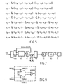
- Fig. 1 diagrammatically shows a transform and encoding arrangement for video signals;
- Fig. 2 shows at which instants these signals are sampled. The Figure also shows the signal samples which together form a block;
- Figure 4 shows an 8x8 DCT transform matrix;
- Figure 5 shows the relationship between a group of 8 input samples xi,k and 8 transformation coefficients Pi k;
- Figure 6 shows a diagram representing a new DCT-algorithm;
- Figure 7 shows the DCT arrangement according to the invention based on the algorithm of Figure 6;
- Figure 8 shows a further embodiment of the DCT arrangement of Figure 7;
- Figure 9 shows a selection circuit for use in the arrangement of Figure 8;
- Figure 10 shows a diagram to explain the operation of the DCT arrangement of Figure 8; and
- Figure 11 shows an IDC arrangement according to the invention.
- Figure 1 shows diagrammatically a transform and encoding arrangement for vide. signals. It comprises a
video signal source 1 supplying.a video signal x̂(t). This signal is applied to asampling circuit 2 which takes samples x(qT) from this video signal under the control of sampling pulses S(qT). In this case there applies that q = ..., -1, 0, 1, 2, ... and that the sampling pulses occur at a frequency fs = 1/T. These video signal samples are then supplied to an analog-to-digital converter 3 which supplies the digital video signal samples x(q). These samples are applied in their turn to a transform andencoding arrangement 4 for generating the desired transformation weighting factors. It comprises more specifically atransform arrangement 5 which receives the video signal samples x(q) and converts them into transform weighting factors y(m). These are subsequently applied to a variableword length encoder 6 which converts each transform weighting factor into a code word z(m) of suitable word length. It comprises anauxiliary encoder 61 which receives the transform weighting factors and ensures the actual encoding. The word length of the code word z(m) is determined by a quantity b(j) which is supplied by abit assignment memory 62. This auxiliary encoder thus supplies code words z(m) varying in length and also ensures that given transform weighting factors y(m) are ignored in that no bit is made available for their encoding. A particularly favourable embodiment of theencoder 6 is described inReference 6. It is to be noted that the samples taken from a video signal and hence from a video picture are shown diagrammatically by means of dots in Figure 2. - An embodiment of the
transform arrangement 5 is shown for the sake of completeness in Figure 3. It is provided with a block-formingcircuit 7 and atransform circuit 8. The block-formingcircuit 7 partitions a picture into blocks of NxN picture elements (video signal samples), for example, in the manner as shown for N=8 in Figure 2. To this end it has aninput 70 which receives the successively occurring video signal samples x(q). A cascade arrangement of N-1 (=7) delay lines 71(.) each having a capacity of R-8 video signal samples is connected to this input. R is the number of video signal samples of a television line. Theinput 70 of this block-formingcircuit 7 and the outputs of each delay line 71 (.) are connected via AND-gate circuits 72(.) to inputs of anOR-gate circuit 73. Each AND-gate circuit also receives 8 control pulses in such a manner that first 8 video signal samples are applied from the delay line 71(7) to the transform circuit, then 8 video signal samples from the delay line 71(6), then 8 video signal samples from the delay line 71 (5), and so forth. These control pulses are generated by a modulo 64 counter 74 to which the sampling pulses are applied. Adecoding network 75 having eight outputs 75 (.) which are connected to inputs of the AND-gate circuits is connected to this counter 74. This decoding network supplies a logic !'1" at the output 75(7) each time the counter has one of the counting positions 1,2,3,...8. A logic "1" occurs at the output 75(6) each time the counter has one of the counting positions 9, 10, 11, ... 16 and so forth. In this manner the video signals of a block occur successively and row by row at the output of theOR-gate circuit 73. - The
transform circuit 8 is constituted by afirst transformer 9, amemory 10 and asecond transformer 11. These transformers have the same structure and are each constituted by a DCT arrangement. In this case thetransformer 9 supplies the product matrix P = XA (see expression (3)) which consists of the coefficients pi,k. These coefficients are written row by row into thememory 10 under the control of acontrol circuit 12 and read from this memory column by column. In this manner the transposed product matrix PT is obtained which is applied to thetransformer 11. - In the
transfnrmer 
- In the above case N=8 so that q=16. Now it holds, for instance that ai,k=2/(N √2) which for N=8 is equal to 2/N cos(4 π/16) which is equal to C4 16.
- A diagram representing the algorithm worked out for N=8 in Figure 5 is shown in Figure 6. It appears from this Figure that for calculating the coefficients pi,k it is possible to first add or subtract those video signal samples which have to be multiplied by equal transform elements Cm q. Only after that the multiplication is really performed. It is also apparent from Figure 6 that if N=8, not more than 22 multiplications, 14 additions and 20 accumulation operations are required per group of eight coefficients. In this respect it is to be noted that two or more multiplications do not occur in any branch of the diagram, which property is important for determining the word length of the intermediate results. In Figure 6 these intermediate results are denoted by the characters u, v, w, z.
- An embodiment of the DCT arrangement whose implementation is based on the new DCT algorithm shown in Figure 6 is shown in Figure 7. It comprises a
shuffle circuit 903 to which the video signal samples are applied in the sequence xi,0, xi,2' ... xi,7. It supplies the same video signal samples but in a different sequence, more specifically as follows xi,0, xi,7 xi,3, xi,4, xi,1, xi,6, xi,2, xi,5. In this sequence they are applied via aninput 901 to acombination circuit 90. Auxiliary samples are also applied thereto via aninput 902. Addition and subtraction operations are performed on these video signal samples and auxiliary samples so that the sum and difference samples denoted by u0 to u7 inclusive in Figure 6 and bracketed in Figure 5 are obtained. These samples are applied to aselection circuit 91 which applies the sum samples u0, u1, u 2, u3, v0, v1 shown in Figure 6 as auxiliary samples to theinput 902 of thecombination circuit 90. The difference samples u4, u 5, u 6, u7, v 2, v 3, w1 as well as the sum sample w0 are applied as transfer samples to a multiplier circuit.92 in which these transfer samples are multiplied by the associated transform elements shown in Figure 6. The product samples z0 to z21 inclusive shown in Figure 6 are thereby obtained. These are applied to anaccumulator circuit 93 which, as is shown in Figure 6, adds given product samples together to obtain the desired coefficients pi,m. These coefficients may be stored temporarily in abuffer memory 94. - In the embodiment shown a
memory circuit 95 as a buffer circuit is incorporated for practical reasons between theselection circuit 91 and themultiplier circuit 92. This has been done because the rate at which mathematical operations must be performed inthecombination circuit 90 can be lower than the rate at which mathematical operations must be performed in themultiplier circuit 92. - Figure 8 shows a more detailed embodiment of the DCT arrangement. The operation of this arrangement is diagrammatically shown in Figure 10. More particularly the first column in Figure 10 indicates the reference numbers of a number of memories present in Figure 8 and the other columns represent the contents of these memories after a clock pulse has occurred. These clock pulses are enumerated 1 to 53, inclusive in the first row. In this Figure the indices i as used in the foregoing as well as in figure 6 have been omitted for the video signal samples and for the coefficients. It is to be noted that in this Figure 10 a dash "-" means that the content of the relevant memory is unchanged.
- In the DCT arrangement which is shown in Figure 8 the
shuffle circuit 903 is constituted by two memories 903 (.) with addressable memory locations ; for example, RAMs. Each of them receives the video signal samples xi,k· These memories are controlled by write and read address commands WRj and Rj in such a manner that the presented video signal samples are written into one of them, while simultaneously the video signal samples present in the other memory are read therefrom. The video signal samples xi,0' xi,3' xi,1, xi,2 read from this memory in response to one of theclock pulses combination circuit 90 in a buffer memory 904(1) which may be formed as a latch and is controlled by a latch enable command LE1, The video signal samples xi,7, xi,4, xi,6, xi,5 read from this memory 903(.) in response to one of theclock pulses combination circuit 90 to latch 904(2) which is controlled by latch enable command LE2. The actual contents of the two latches 904(.) are applied in response to eachfurther clock pulse - The selection circuits 905(.) are built up in the same manner and each have two inputs 9051(.) and 9052(.) The inputs 9052(.) receive the video signal sample which is stored in latch 904(.) and the inputs 9051(.) receive auxiliary samples which are applied via inputs 902(.) to the combination circuit. These selection circuits 905(.) also receive two control commands SEL1 and SEL2 which ensure that either the video signal sample from latch 904(.) or the auxiliary sample at input 9051(.) is stored in latch 906(.). As is shown in Figure 9, this selection circuit may be simply formed by two AND-gate circuits 9O53(.) and 9054(.) and an OR-gate circuit 9055 (.). In this way it is achieved that, for example, after the occurrence of
clock pulse 6 latches 906(.) comprise the video signal samples xi,0 and xi 7, whilst these latches comprise the auxiliary samples u1 and u2 after the occurrence of, for example,clock pulse 36. - The samples present in the latches 906(.) are applied to an adder-
subtractor circuit 907 which is controlled by an adding command AC and a subtraction command SC. This circuit subtracts each time the two samples present in the latches 906(1) and 906(2) so that the difference samples u7, u4, u6, u5' v3' v2' w 1 are obtained. They are also added together so that the sum samples u0' u3' u1, u2, v0, v1' w0 are obtained. Each sample is applied to theselection circuit 91 where such a sample, in response to the occurrence of a latch enable command LE4 (coinciding with theclock pulses latch 910. Each difference sample and the sum sample w0 is subsequently applied directly as a transfer sample to thebuffer circuit 95. The other sum samples are temporarily stored in one of the three latches 911(.) which are controlled by the latch enable commands LES5, LE6 and LE7, respectively. Figure 10 shows in detail which sum sample is stored in which latch. It is also apparent from this Figure when this happens and when such sum samples are applied as auxiliary samples to the latches 906(.) For example, the sum samples u0 and u3 are stored in response toclock pulse 30 in the latches 906(1) and 906(2), respectively, so as to subsequently supply the difference sample v3 which in response toclock pulse 33 is stored inlatch 910 to be transferred in its turn to thebuffer circuit 95 in response toclock pulse 34. The sum sample u0 supplied in response to the two sum samples u0 and u3 by the adder-subtractar circuit is stored inlatch 910 in response toclock pulse 36 and is subsequently stored in latch 911(1) in response toclock pulse 37, and so forth, As is apparent from Figure 10, all eight video signal samples xi,0 to xi,7 inclusive are converted after 52 clock pulses into the eight transfer samples u4, u5, u6, u7, v2, v3, v0' w1 which are all present in the store 951(1) at that instant. - The
buffer circuit 95 is built up in the same manner as theshuffle circuit 903. It also comprises two RAM's 951(.) which are controlled by the read and write address commands R and WRj, respectively. Also in this case the control is such that all transfer samples which are calculated, starting from a given group of video signal samples xi,k which are present in one of the memories 9031(.), are written into one of the memories 951 (.). In Figure 10 it is assumed that the actually calculated transfer samples are written into memory 951(1) and that the memory 951(2) comprises all transfer samples which are calculated in the previous cycle of 52 clock pulses. As is shown in Figure 10 this means that after the fourth clock pulse the memory 951(2) comprises a completely new set of transfer samples. - To calculate the desired transformation coefficients, these transfer samples are also applied to the
multiplier circuit 92. This circuit comprises twofurther latches multiplier 923 which receives the transform elements Cm from amemory 924, for example, a ROM is incorporated between the two latches. This ROM is controlled by an address command R5. The content oflatch 922 is applied to theaccumulator circuit 93 which is built up in known manner and comprises anadder circuit 931 and amemory 932. This memory, which can only comprise one word supplied by theadder 931, is reset by means of a reset command RES. The sum number supplied by theadder 931 is written into this memory in response to a write command WR5. This sum number may also be written into thebuffer memory 94 by means of a further write command BE. - As is shown in Figure 10, the transfer samples u7, u4, u6, u5 are written into the
latch 921 in response to theclock pulses accumulator circuit 93 so that the transform coefficient Pi,1 can be written into thebuffer memory 94 in response toclock pulse 16. Correspondingly, the other transform coefficients are obtained so that thisbuffer memory 94, in response toclock pulse 52, comprises a completely new set of eight transform coefficients. As is shown in Figure 10 the same situation occurred at the instant after the occurrence of the fourth clock pulse. - The above-mentioned clock pulses occur at a rate which is, for example, six times as high as the sampling frequency f s at which the video signal samples occur. With the aid of a
frequency multiplier circuit 96 they are derived from the sampling pulses S(qT) which are supplied by apulse source 97. These clock pulses are also used to generate the various commands. They are therefore applied to a modulo-48counter 98 whose counting position is applied as an address to amemory 99 with addressable memory locations; for example, a ROM. Each memory location comprises the values "0" and "1" of all commands. These commands are applied to the different elements by means of abus 100 consisting of many lines. - As already expressed in the opening paragraph, an inverse transformation is to be performed on the ultimately obtained weighting factors in order to recover the original picture elements. This inverse transformation requires an inverse discrete cosine transformation. It can be realized by means of the IDCT arrangement shown in Figure 11. It differs from the DCT arrangement of Figure 7 exclusively in the location of the
circuit combinations
Claims (5)
1. An arrangement for real-time calculation of the discrete cosine transformation coefficients of a group of N signal samples of a time-discrete input signal, comprising:
- combination means receiving the signal samples as well as a number of auxiliary samples and adapted to add and subtract predetermined combinations of said samples for generating sum and difference samples;
- selection means receiving the sum and difference samples and supplying said auxiliary samples as well as transfer samples, the auxiliary samples being constituted by selected ones of the sum and difference samples and the transfer samples being constituted by the remaining sum and difference samples;
- multiplication means receiving the transfer samples and multiplying each by only one weighting factor selected from a plurality of predetermined weighting factors for generating product samples; and
- accumulator means receiving the product samples and adapted to accumulate given samples of these product samples for generating the coefficients.
2. An arrangement for real-time calculation of the N inverse discrete cosine transformation signal samples of a time-discrete signal from a group of N discrete cosine transformation coefficients, comprising
- multiplication means receiving the coefficients and multiplying each by only one weighting factor selected from a plurality of predetermined weighting factors for generating product samples;
- accumulator means receiving the product samples and adapted to add each time given samples of these product samples together for generating accumulation samples;
- combination means receiving the accumulation samples as well as a number of auxiliary samples and adapted to add and subtract predetermined combinations of the said samples for generating sum and difference samples; and
- selection means receiving the sum and difference samples and supplying said auxiliary samples as well as transfer samples, the auxiliary samples being constituted selected ones of the sum and difference samples and the transfer samples being constituted by the remaining sum and difference samples.
3. An arrangement as claimed in Claim 1, wherein the auxiliary samples are constituted by sum samples.
4. An arrangement as claimed in Claim 1 or 2 further comprising shuffle means to which the N-signal samples or the N-coefficients are applied in a first sequence and which supplies these signal samples or coefficients in a second sequence which corresponds to the combinations of samples to be added or to be subtracted.
5. An arrangement as claimed in Claim 1 or 2 wherein the combination means comprises two memories for storing a first and a subsequent second sample, which samples are applied to an adder-subtractor circuit and are supplied by a selection circuit which receives signal samples or the accumulation samples and the auxiliary samples and which applies them selectively to the two memories.
Applications Claiming Priority (2)
| Application Number | Priority Date | Filing Date | Title |
|---|---|---|---|
| NL8601183 | 1986-05-12 | ||
| NL8601183A NL8601183A (en) | 1986-05-12 | 1986-05-12 | DISCRETE COSINUS TRANSFORMATION DEVICE. |
Publications (1)
| Publication Number | Publication Date |
|---|---|
| EP0245903A1 true EP0245903A1 (en) | 1987-11-19 |
Family
ID=19847993
Family Applications (1)
| Application Number | Title | Priority Date | Filing Date |
|---|---|---|---|
| EP87200830A Withdrawn EP0245903A1 (en) | 1986-05-12 | 1987-05-06 | Discrete cosine transform arrangement |
Country Status (6)
| Country | Link |
|---|---|
| US (1) | US4837724A (en) |
| EP (1) | EP0245903A1 (en) |
| JP (1) | JPS62269519A (en) |
| KR (1) | KR870011803A (en) |
| CN (1) | CN1009034B (en) |
| NL (1) | NL8601183A (en) |
Cited By (3)
| Publication number | Priority date | Publication date | Assignee | Title |
|---|---|---|---|---|
| US5008848A (en) * | 1989-05-30 | 1991-04-16 | North American Philips Corporation | Circuit for performing S-transform |
| DE4038240A1 (en) * | 1989-12-01 | 1991-06-06 | Ricoh Kk | PROCESSOR FOR CARRYING OUT AN ORTHOGONAL TRANSFORMATION |
| US5359549A (en) * | 1989-12-01 | 1994-10-25 | Ricoh Company, Ltd. | Orthogonal transformation processor for compressing information |
Families Citing this family (21)
| Publication number | Priority date | Publication date | Assignee | Title |
|---|---|---|---|---|
| FR2626693B1 (en) * | 1987-12-03 | 1990-08-10 | France Etat | BUFFER MEMORY DEVICE AND METHOD, PARTICULARLY FOR LINE-COLUMN MATRIX TRANSPOSITION OF DATA SEQUENCES |
| US4941043A (en) * | 1988-06-14 | 1990-07-10 | Siemens Aktiengesellschaft | Method for reducing blocking artifacts in video scene coding with discrete cosine transformation (DCT) at a low data rate |
| DE69010366T2 (en) * | 1989-03-30 | 1994-12-01 | Canon Kk | Still video camera. |
| US4974078A (en) * | 1989-11-13 | 1990-11-27 | Eastman Kodak Company | Digital compression method and system with improved coding efficiency |
| TW223690B (en) * | 1991-02-13 | 1994-05-11 | Ampex | |
| FR2681962B1 (en) * | 1991-09-30 | 1993-12-24 | Sgs Thomson Microelectronics Sa | METHOD AND CIRCUIT FOR PROCESSING DATA BY COSINUS TRANSFORM. |
| US5539836A (en) * | 1991-12-20 | 1996-07-23 | Alaris Inc. | Method and apparatus for the realization of two-dimensional discrete cosine transform for an 8*8 image fragment |
| US5394349A (en) * | 1992-07-10 | 1995-02-28 | Xing Technology Corporation | Fast inverse discrete transform using subwords for decompression of information |
| CA2094524A1 (en) * | 1992-07-30 | 1994-01-31 | Ephraim Feig | Digital image processor for color image compression |
| US5345408A (en) * | 1993-04-19 | 1994-09-06 | Gi Corporation | Inverse discrete cosine transform processor |
| US5467131A (en) * | 1993-12-30 | 1995-11-14 | Hewlett-Packard Company | Method and apparatus for fast digital signal decoding |
| CN1076838C (en) * | 1994-08-19 | 2001-12-26 | 财团法人工业技术研究院 | Transposed memory for discrete cosine transform/converse discrete cosine transform circuit |
| KR100235064B1 (en) * | 1996-05-23 | 1999-12-15 | 전주범 | Apparatus for coding objects using block based coding technique |
| US5818535A (en) * | 1996-09-30 | 1998-10-06 | Alaris, Inc. | Method and apparatus for adaptive hybrid motion video compression and decompression |
| US7007054B1 (en) | 2000-10-23 | 2006-02-28 | International Business Machines Corporation | Faster discrete cosine transforms using scaled terms |
| US6766341B1 (en) | 2000-10-23 | 2004-07-20 | International Business Machines Corporation | Faster transforms using scaled terms |
| US6961473B1 (en) * | 2000-10-23 | 2005-11-01 | International Business Machines Corporation | Faster transforms using early aborts and precision refinements |
| EP1445706A1 (en) * | 2003-01-18 | 2004-08-11 | Deutsche Thomson-Brandt Gmbh | Method, apparatus, and computer program for performing a modified discrete cosine transform |
| US7725516B2 (en) * | 2005-10-05 | 2010-05-25 | Qualcomm Incorporated | Fast DCT algorithm for DSP with VLIW architecture |
| CN101989253B (en) * | 2009-07-31 | 2012-08-29 | 鸿富锦精密工业(深圳)有限公司 | Discrete cosine conversion circuit and image processing device using same |
| JPWO2013042249A1 (en) * | 2011-09-22 | 2015-03-26 | 富士通株式会社 | Fast Fourier transform circuit |
Citations (4)
| Publication number | Priority date | Publication date | Assignee | Title |
|---|---|---|---|---|
| US4385363A (en) * | 1978-12-15 | 1983-05-24 | Compression Labs, Inc. | Discrete cosine transformer |
| EP0154340A1 (en) * | 1984-03-09 | 1985-09-11 | Alcatel Cit | Inverse discrete cosine transform processor |
| EP0154341A1 (en) * | 1984-03-09 | 1985-09-11 | Alcatel Cit | Discrete cosine transform processor |
| EP0206847A1 (en) * | 1985-05-03 | 1986-12-30 | Thomson Grand Public | Cosine transform calculating devices, picture coding and decoding device comprising such calculating devices |
Family Cites Families (6)
| Publication number | Priority date | Publication date | Assignee | Title |
|---|---|---|---|---|
| US4196448A (en) * | 1978-05-15 | 1980-04-01 | The United States Of America As Represented By The Secretary Of The Navy | TV bandwidth reduction system using a hybrid discrete cosine DPCM |
| US4225850A (en) * | 1978-11-15 | 1980-09-30 | Rockwell International Corporation | Non-fingerprint region indicator |
| NL8003873A (en) * | 1980-07-04 | 1982-02-01 | Philips Nv | METHOD FOR DIGITIZING A TIME-DISCREET VIDEO SIGNAL USING AN IMAGE TRANSFORMATION |
| NL8004521A (en) * | 1980-08-08 | 1982-03-01 | Philips Nv | METHOD FOR DIGITIZING A COLOR VIDEO SIGNAL |
| US4449194A (en) * | 1981-09-25 | 1984-05-15 | Motorola Inc. | Multiple point, discrete cosine processor |
| US4445248A (en) * | 1982-06-04 | 1984-05-01 | International Hardware, Inc. | Rotary stripper |
-
1986
- 1986-05-12 NL NL8601183A patent/NL8601183A/en not_active Application Discontinuation
-
1987
- 1987-05-06 US US07/047,795 patent/US4837724A/en not_active Expired - Fee Related
- 1987-05-06 EP EP87200830A patent/EP0245903A1/en not_active Withdrawn
- 1987-05-09 JP JP62111718A patent/JPS62269519A/en active Pending
- 1987-05-09 CN CN87103462A patent/CN1009034B/en not_active Expired
- 1987-05-11 KR KR870004588A patent/KR870011803A/en not_active Application Discontinuation
Patent Citations (4)
| Publication number | Priority date | Publication date | Assignee | Title |
|---|---|---|---|---|
| US4385363A (en) * | 1978-12-15 | 1983-05-24 | Compression Labs, Inc. | Discrete cosine transformer |
| EP0154340A1 (en) * | 1984-03-09 | 1985-09-11 | Alcatel Cit | Inverse discrete cosine transform processor |
| EP0154341A1 (en) * | 1984-03-09 | 1985-09-11 | Alcatel Cit | Discrete cosine transform processor |
| EP0206847A1 (en) * | 1985-05-03 | 1986-12-30 | Thomson Grand Public | Cosine transform calculating devices, picture coding and decoding device comprising such calculating devices |
Non-Patent Citations (1)
| Title |
|---|
| IEEE TRANSACTIONS ON ELECTROMAGNETIC COMPATIBILITY, vol. EMC-24, no. 2, May 1982, pages 278-286, IEEE, New York, US; A. JALALI et al.: "A high-speed FDCT processor for real-time processing of NTSC color TV signal" * |
Cited By (5)
| Publication number | Priority date | Publication date | Assignee | Title |
|---|---|---|---|---|
| US5008848A (en) * | 1989-05-30 | 1991-04-16 | North American Philips Corporation | Circuit for performing S-transform |
| DE4038240A1 (en) * | 1989-12-01 | 1991-06-06 | Ricoh Kk | PROCESSOR FOR CARRYING OUT AN ORTHOGONAL TRANSFORMATION |
| US5268853A (en) * | 1989-12-01 | 1993-12-07 | Ricoh Company, Ltd. | Orthogonal transformation processor for compressing information |
| US5331585A (en) * | 1989-12-01 | 1994-07-19 | Ricoh Company, Ltd. | Orthogonal transformation processor for compressing information |
| US5359549A (en) * | 1989-12-01 | 1994-10-25 | Ricoh Company, Ltd. | Orthogonal transformation processor for compressing information |
Also Published As
| Publication number | Publication date |
|---|---|
| JPS62269519A (en) | 1987-11-24 |
| KR870011803A (en) | 1987-12-26 |
| US4837724A (en) | 1989-06-06 |
| CN87103462A (en) | 1987-11-25 |
| CN1009034B (en) | 1990-08-01 |
| NL8601183A (en) | 1987-12-01 |
Similar Documents
| Publication | Publication Date | Title |
|---|---|---|
| EP0245903A1 (en) | Discrete cosine transform arrangement | |
| US4831440A (en) | Television transmission system using transform coding | |
| EP0353223B1 (en) | Two-dimensional discrete cosine transform processor | |
| US4912668A (en) | Mono-dimensional reverse cosine transform computing device | |
| JP2646778B2 (en) | Digital signal processor | |
| Madisetti et al. | A 100 MHz 2-D 8/spl times/8 DCT/IDCT processor for HDTV applications | |
| JP2628493B2 (en) | Image coding device and image decoding device provided with cosine transform calculation device, calculation device and the like | |
| EP0275979B1 (en) | Circuit for computing the quantized coefficient discrete cosine transform of digital signal samples | |
| US5325215A (en) | Matrix multiplier and picture transforming coder using the same | |
| US5331585A (en) | Orthogonal transformation processor for compressing information | |
| US5471412A (en) | Recycling and parallel processing method and apparatus for performing discrete cosine transform and its inverse | |
| JP2630801B2 (en) | One-dimensional linear image converter | |
| US4736440A (en) | Process for the processing of digitized signals representing an original image | |
| US6003058A (en) | Apparatus and methods for performing arithimetic operations on vectors and/or matrices | |
| US5847980A (en) | Product-summing arithmetic circuit | |
| EP0511606A2 (en) | Parallel interpolator for high speed digital image enlargement | |
| US5999958A (en) | Device for computing discrete cosine transform and inverse discrete cosine transform | |
| KR100212268B1 (en) | Idct system using lee's algorithm | |
| JPH07200539A (en) | Two-dimensional dct arithmetic unit | |
| JP3970442B2 (en) | Discrete cosine transform device and inverse discrete cosine transform device | |
| JP2802158B2 (en) | Inverse orthogonal transform method and inverse orthogonal transform circuit | |
| US5864494A (en) | Discrete cosine transformer and inverse discrete cosine transformer | |
| KR100202567B1 (en) | An arithmetic apparatus for high speed idct | |
| JP3697716B2 (en) | Matrix data multiplier | |
| JP2960595B2 (en) | Digital signal processor |
Legal Events
| Date | Code | Title | Description |
|---|---|---|---|
| PUAI | Public reference made under article 153(3) epc to a published international application that has entered the european phase |
Free format text: ORIGINAL CODE: 0009012 |
|
| AK | Designated contracting states |
Kind code of ref document: A1 Designated state(s): AT DE FR GB IT |
|
| 17P | Request for examination filed |
Effective date: 19880505 |
|
| 17Q | First examination report despatched |
Effective date: 19891026 |
|
| STAA | Information on the status of an ep patent application or granted ep patent |
Free format text: STATUS: THE APPLICATION IS DEEMED TO BE WITHDRAWN |
|
| 18D | Application deemed to be withdrawn |
Effective date: 19910423 |
|
| RIN1 | Information on inventor provided before grant (corrected) |
Inventor name: VISSER, CORNELIS P. Inventor name: BORGERS, STEPHANUS M. C. |