EP0244629B1 - Radio transmission system having simplified error coding circuitry and fast channel switching - Google Patents
Radio transmission system having simplified error coding circuitry and fast channel switching Download PDFInfo
- Publication number
- EP0244629B1 EP0244629B1 EP87104681A EP87104681A EP0244629B1 EP 0244629 B1 EP0244629 B1 EP 0244629B1 EP 87104681 A EP87104681 A EP 87104681A EP 87104681 A EP87104681 A EP 87104681A EP 0244629 B1 EP0244629 B1 EP 0244629B1
- Authority
- EP
- European Patent Office
- Prior art keywords
- channel
- error correcting
- time
- bits
- error
- Prior art date
- Legal status (The legal status is an assumption and is not a legal conclusion. Google has not performed a legal analysis and makes no representation as to the accuracy of the status listed.)
- Expired - Lifetime
Links
- 230000005540 biological transmission Effects 0.000 title claims description 24
- 239000002131 composite material Substances 0.000 claims description 22
- 238000012545 processing Methods 0.000 claims description 19
- 238000009432 framing Methods 0.000 claims description 16
- 238000007906 compression Methods 0.000 claims description 14
- 230000006835 compression Effects 0.000 claims description 12
- 230000004044 response Effects 0.000 claims description 5
- 238000001514 detection method Methods 0.000 claims description 4
- 238000000034 method Methods 0.000 description 7
- 238000003780 insertion Methods 0.000 description 6
- 230000037431 insertion Effects 0.000 description 6
- 230000008569 process Effects 0.000 description 5
- 238000010586 diagram Methods 0.000 description 4
- 238000005562 fading Methods 0.000 description 4
- 230000001360 synchronised effect Effects 0.000 description 3
- 238000012360 testing method Methods 0.000 description 3
- 238000012937 correction Methods 0.000 description 2
- 230000008878 coupling Effects 0.000 description 2
- 238000010168 coupling process Methods 0.000 description 2
- 238000005859 coupling reaction Methods 0.000 description 2
- 230000000694 effects Effects 0.000 description 2
- 230000006870 function Effects 0.000 description 2
- 108091026890 Coding region Proteins 0.000 description 1
- 230000009471 action Effects 0.000 description 1
- 238000006243 chemical reaction Methods 0.000 description 1
- 230000003111 delayed effect Effects 0.000 description 1
- 238000009795 derivation Methods 0.000 description 1
- 238000005516 engineering process Methods 0.000 description 1
- 238000000605 extraction Methods 0.000 description 1
- 238000012986 modification Methods 0.000 description 1
- 230000004048 modification Effects 0.000 description 1
- 230000010355 oscillation Effects 0.000 description 1
Images

Classifications
-
- H—ELECTRICITY
- H04—ELECTRIC COMMUNICATION TECHNIQUE
- H04L—TRANSMISSION OF DIGITAL INFORMATION, e.g. TELEGRAPHIC COMMUNICATION
- H04L1/00—Arrangements for detecting or preventing errors in the information received
- H04L1/22—Arrangements for detecting or preventing errors in the information received using redundant apparatus to increase reliability
-
- H—ELECTRICITY
- H04—ELECTRIC COMMUNICATION TECHNIQUE
- H04L—TRANSMISSION OF DIGITAL INFORMATION, e.g. TELEGRAPHIC COMMUNICATION
- H04L1/00—Arrangements for detecting or preventing errors in the information received
Definitions
- the present invention relates to radio transmission systems, and more particularly to a digital radio transmission system that simplifies circuitry for forward error correcting encoders and reduces the period of switching between regular and standby channels in the event of a fault due to fading.
- the conventional digital microwave radio transmission system comprises a bipolar-to-unipolar converter for converting the bipolar time-division digital signals transmitted over coaxial cables from a switching node to unipolar TDM digital signals and a transmit digital processing unit which performs time compression on a block of a prescribed number of the incoming data bits and inserts additional bits for channel supervision and switching to form a series of composite bits for transmission to a receiving station where the signal is processed in a manner inverse to that of the transmitting station.
- the composite bits are fed to a forward error correcting encoder where the composite bits are again time-compressed to leave a time slot and error computations are performed on the time-compressed composite bits according to an error encoding theorem to generate an error correcting code which is inserted to the time slot to form a block code.
- the error decoding process at the receiving station is a process inverse to that of the error encoding process and two stages of time expansion are required for expanding the time scale of the composite bits following the execution of an error decoding process and for expanding the time scale of the compressed data bits after extraction of the additional bits.
- time compression process requires a memory, a phase-locked loop and a counter for matching different data rates, they must be duplicated for insertion of control bits and insertion of error correcting codes.
- time expansion process requires a similar arrangement, and therefore phase-locked loops and counters must be duplicated for the error correcting decoder and receive digital processing unit, although such duplications serve to minimize the timing disruption in the sequence of computations of the forward error correcting encoder if channel switching is effected at a point between the output of a regular-channel transmit digital processing unit and the input of a standby-channel forward error correcting encoder in the event of a fault in the regular channel.
- GB-A-1,536,337 describes a digital transmission system using an m-bit serial store for speed conversion to insert parity bits.
- US-A-3,471,830 describes a transmission system where an n-digit data sequence is converted to a format in which the k-digit parity check sequence is combined with the n-digit sequence.
- a standby channel is usually provided for a plurality of regular channels. If a bit error rate of a regular channel exceeds a predetermined level due to fading, the regular channel is treated as faulty and the output of the transmit digital processing unit is switched into circuit with the forward error correcting encoder of the standby channel and this switching occurs at the output of a regular-channel transmit digital processing unit to the input of a standby-channel forward error correcting encoder.
- the single time compression operation simplifies error encoding circuitry, it is highly likely that a brief disruption occurs in the sequence of computations in the standby-channel forward error correcting encoder, causing what is known as "word-sync misalignment".
- the present invention eliminates this problem by causing a frame synchronizer at a receiving station to derive a timing signal and causing a forward error correcting decoding sequence to be synchronized with the derived timing signal. Since frame acquisition time is much shorter than the self-derived word acquisition time for error encoding and decoding operations, frame-derived word synchronization can be reestablished in a short period of time at the receiving station.
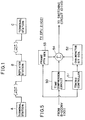
- the digital radio transmission system of the present invention extends between microwave terminal stations A and C by way of a repeater station B.
- Remote subscriber terminals may be directly connected to terminal stations A and C, but usually telecommunication switching systems are interfaced to these radio stations through time-division multiplexers for transmission of TDM digital signals and through time-division demultiplexers for reception of such TDM signals.
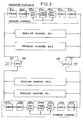
- each radio station includes a set of N regular channels and a standby channel for each direction of transmission.
- the terminal station A comprises Nos. 1 and 2 transmit regular channels and a transmit standby channel and Nos. 1 and 2 receive regular channels and a receive standby channel. All control functions are centralized in a controller 20.
- Each of the transmit channels is identically composed of a bipolar-to-unipolar converter 1 which converts the signal received through an associated time-division multiplexer, not shown, in bipolar form over a coaxial cable to unipolar form for radio transmission.
- a transmit digital processing unit (DPU) 2 is connected to the output of bipolar-to-unipolar converter 1 for providing digital processing of the unipolar signal in a manner as will be described later.
- the transmit DPU 2 provides time compression on a prescribed number of bits of the incoming unipolar data stream to allow for insertion of additional bits including a parity bit and a framing bit to provide the first level of framing and for insertion of a time slot with a string of all binary zero's. The time-compressed data bits and the additional bits from composite bits.
- a forward error correcting (FEC) encoder 3 is connected to the output of transmit DPU 2 of the same channel to insert an error-correcting code to the time slot so that signals detected as being in error are automatically corrected at the receiving stations before delivery to remote terminals.
- a digital modulator 4 such as 16-QAM modulator and a transmitter 5 are cascaded to the output FEC encoder 3 for transmitting a modulated digital signal on a particular carrier frequency.
- the outputs of transmitters 5 are connected together to an input terminal of a duplexer 6 and thence to a microwave antenna 7.
- the Nos. 1 and 2 regular transmit channels include electromechanical switches 8. Under normal conditions, bipolar digital signals from the multiplexers are coupled to the bipolar-to-unipolar converters 1 of the associated regular channels and a test signal from a pilot generator 9 is coupled to the bipolar-to-unipolar converter 1a of the standby transmit channel.
- the electromechanical switches 8 are operated when a fault condition occurs in the B-U converters 1 and transmit DPUs 2 by coupling the output of the associated multiplexer to the standby transmit channel and decoupling the test signal from the standby channel. Switches 8 are also operated when a fault condition occurs in unipolar-to-bipolar (U-B) converters and receive DPUs of the receiving station C.
- Switching control signals for operating the electromechanical switches 8 are supplied from the controller 20 as it receives an alarm signal from a receive DPU of the channel associated with the transmit channel in a manner as will be described. Further included are solid-state channel switching circuits 10 which are respectively connected between the transmit digital processing units 2 and FEC encoders 3a of the standby channel and the Nos. 1 and 2 regular channels. Under normal conditions, the outputs of transmit DPUs 2a, 2b and 2c are connected respectively to the FEC encoders 3a, 3b and 3c.
- the controller 20 is notified of this fact by a control signal inserted in a predetermined time slot of the TDM superframe through a receive channel which forms a pair of "go" and "return” paths with the faulty transmit channel to cause the switching circuit 10a of the standby transmit channel to connect the output of transmit DPU 2 of the faulty channel into circuit with the input of FEC encoder 3a of the standby channel.
- the output signal of the transmit DPU 2 of the faulty channel is transmitted simultaneously over the standby and faulty channels until bit synchronization is reestablished in the activated standby channel at the receiving station C.
- Each of the receive channels comprises a receiver 11 tuned to a particular frequency band, a demodulator 12 and a forward error correcting decoder 13 which are cascaded to the output of duplexer 6.
- the FEC decoder 13 performs error correcting computations on the composite bits of each block code recovered by demodulator 12 using the error correcting code contained therein according to a known error decoding theorem and supplies an error-corrected signal without expanding the error corrected composite bits to a frame synchronizer 14 which detects framing bits from the output of FEC decoder 13 to allow frame timing of the channel to be synchronized with the data stream and to supply a signal indicative of this frame timing to the controller 20.
- the synchronized data stream is normally coupled to the receive DPU 15 of the same channel.
- Each receive DPU 15 removes the overhead bits from the input signal so that it contains only data bits and provides expansion of the time scale of data bits to recover the original signal.
- Each receive DPU 15 includes a fault detection circuit that monitors the bit error rate of the associated channel and an alarm signal transmitted in a superframe time slot from terminal station C and communicates this fact to the controller 20, which determines which one of the transmit and receive channels is faulty.
- the unipolar output of each receive DPU 15 is converted to bipolar format by an associated unipolar-to-bipolar converter 16.
- the receive channels include electromechanical switches 17 connected respectively to the outputs of Nos. 1 and 2 regular receive channels. Under normal conditions, the outputs of the regular receive channels are coupled to the associated time-division demultiplexers, not shown, while the output of the standby receive channel is coupled to a pilot detector 18 which monitors the test signal transmitted from the pilot generator of terminal station C. If a fault condition occurs in the standby receive channel, pilot detector 18 communicates this fact to the controller 20 to prevent channel switching operation.
- These electromechanical switches 17 are operated when a fault is detected in the receive DPUs and U-B converters of the regular receive channels by coupling the output of U-B converter 16a of the standby channel to the demultiplexer that has been associated with the faulty receive channel.
- the outputs of frame synchronizers 14 are normally connected through solid-state channel switching circuits 19 to the receive DPU's 15 of the same channels.
- Receive DPUs 15 monitor the bit error rate of the associated receive channels. If a faulty condition occurs in a regular receive channel, the receive DPU 15 of this channel communicates this fact to the controller 20 which in turn sends a switching control signal through the transmit DPU 2 associated with the faulty receive channel to the terminal station C. This switching control signal is applied to the controller of the terminal station C to cause channel switching to occur at the transmit end of this faulty receive channel.
- the frame synchronizer 14a of the standby channel attempts to detect a framing bit to establish synchronization.
- the standby frame synchronizer 14a Upon detection of a framing bit, the standby frame synchronizer 14a notifies this fact to the controller 20 to direct the switching circuit 19a of the standby channel to establish bit synchronization. Upon establishment of bit synchronism, the standby channel switching circuit 19a communicates this fact to the controller 20 to operate the faulty channel switching circuit 19 to disconnect the output of the faulty channel frame synchronizer 14 out of circuit with the input of receive DPU 15 which has been associated with it.
- Transmit DPU comprises a time-compression circuit 50 which includes a memory and a phase comparator that detects a phase difference between an input clock signal from a timing controller 51 and a clock input supplied through a gate from a voltage controlled oscillator whose frequency is controlled by the phase difference.
- Input data stream from the associated B-U converter 1 is written into the memory at the clock timing of the timing controller 51 and read out of it at the gated clock timing of the VCO.
- a counter circuit is included in the time compression circuit to count the oscillations of the VCO to disable the gate to compress the time scale of the input data stream.
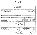
- the input data stream is represented by a series of consecutive (K - 1) data bits designated D1 through D k-1 as illustrated in Fig. 6.
- K - 1 data bits
- D1 through D k-1 data bits designated D1 through D k-1 as illustrated in Fig. 6.
- These data bits are input to the time compression circuit 50 at the transmission rate and delivered therefrom at a compression rate (K-1)/(N-K+1) to allow for insertion of a control field F immediately following the data bit D k-1 to form a composite word of K bits and a time slot of (N-K) bits.
- the control field F is occupied with a parity bit generated by a channel monitor bit generator 52 and with a framing bit generated by a frame pattern generator 53.
- a multiplexer 54 under control of timing controller 51 to generate a series of N unipolar bits comprising (K-1) data bits, one control bit and a time slot which is a string of (N-K) binary zero's.
- the output of multiplexer 54 is supplied through the switching circuit 10 to the associated FEC encoder 3.
- FEC encoder 3 treats the K-bit of combined data and control bits as information bits by performing computations according to the well known error coding theorem, generates error correcting bits P1 through P n-k and inserts them into the (N-K)-bit time slot of the incoming data stream.
- the output of FEC encoder 3 is therefore a series of N-bit block codes with a code-rate efficiency of K/N. Because of the single time compressing operation by the transmit data processing units 10, the FEC encoders 3 are not required to effect time compression which is provided in the prior art using phase locked loops and counters. Thus, FEC encoders 3 can be simplified and rendered economical.
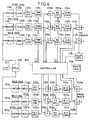
- the repeater station B comprises antennas 30 and 31 respectively pointed towards the antennas of terminal stations A and C, three A-to-C channels for relaying signals from station A to station C and three C-to-A channels for relaying signals from station C to station A.
- A-to-C channels comprise regular channels Nos. 1 and 2 and a standby channel.
- Each of these A-to-C channels are identically composed of a receiver 21a, a demodulator 22a, a forward error correcting decoder 23a, a frame synchronizer 24a, a forward error correcting encoder 25a, a modulator 26a and a transmitter 27a, all of which are cascaded from the output terminal of a duplexer 28 coupled to antenna 30 to the input terminal of a duplexer 29 coupled to antenna 31.
- the FEC decoder 23a performs error correcting computations on the time-compressed codeword according to a well known error decoding theorem to correct bits in error and supplies the error-corrected data stream to frame synchronizer 24a.
- Frame synchronizer 24a detects a frame sync, establish frame alignment with the data bit stream and supplies a frame timing pulse to FEC decoder 23a and FEC encoder 25a to permit them to quickly reestablish word synchronization with the data stream when channel switching takes place in the terminal station A.
- each of the C-to-A channels are identically composed of a receiver 121a, a demodulator 122a, a forward error correcting decoder 123a, a frame synchronizer 124a, a forward error correcting encoder 125a, a modulator 126a and a transmitter 127a, all of which are cascaded from the output terminal of duplexer 29 to the input terminal of duplexer 28.
- Frame synchronizer 124a detects a framing bit and supplies a frame timing pulse to FEC decoder 123a and FEC encoder 125a to permit them to quickly reestablish word synchronization when channel switching takes place in the terminal station C.
- Terminal station C is identically constructed to terminal station A as shown in Fig. 4. Receive channels are tuned respectively to the carrier frequencies of the transmit channels of terminal station A and transmit channels are associated respectively to the receive channels of terminal station A. Parts corresponding to those of Fig. 2 are marked with numerals "1" in the hundredth unit plus corresponding numerals to those in Fig. 2.
- TDM digital signals are transmitted in opposite directions over regular channels between terminal stations A and C. Assume that a bit error rate of the No. 1 transmit channel between terminal station A and repeater station B exceeds a predetermined value due to fading. Recognizing this as a faulty condition, the receive DPU 115b at terminal station C communicates this fact to the station C controller 120. Controller 120 proceeds to check the output of the pilot detector 118 to see if there is no faulty condition in the standby channel from station A to station C. If there is no faulty condition in this A-to-C standby channel, controller 120 supplies a switching control signal to the transmit DPU 102b.
- the transmit DPU 102b inserts a switching control word to a particular superframe control field of the TDM signal transmitted over the No. 1 C-to-A regular channel that forms a pair with the faulty No. 1 A-to-C channel.
- the receive DPU 15b at terminal station A monitors this superframe control field and notifies the controller 20 of the occurrence of a faulty condition in the No. 1 transmit channel of terminal station A and applies switching signals to the channel switching circuits 10a and 10b to simultaneously bring the output of transmit DPU 2b into circuit with the inputs of FEC encoders 3a and 3b, and so the same TDM signal is transmitted simultaneously over the standby channel and the faulty No. 1 channel to terminal station C.
- the present invention avoids this problem by the derivation of a timing signal from the repeater station frame synchronizer 24a for application to the FEC decoder 23a and FEC encoder 25a. Since the bit error rate of the data stream transmitted over the standby channel can be considered negligibly small, frame synchronizer 24a is likely to detect a framing bit in the received data stream in a short period time following the channel switching operation even though its frame synchronization is lost due to the loss of word synchronization in the decoder 23a and reestablishes frame synchronization in a much shorter period of time than would otherwise be required for the standby channel to reestablish word synchronization.
- the frame synchronizer 24a With frame synchronization being reestablished, the frame synchronizer 24a now generates a correct timing pulse and supplies it to FEC decoder 23a and FEC encoder 25a to allow them to realign their word timing with the data stream to resume their error correcting functions in a short period of time.
- FEC decoder 23a and FEC encoder 25a In the receiving terminal station C, a similar action takes place in the FEC decoder 113a to that of FEC decoder 23a to reestablish word-sync alignment in a much shorter period of time that would otherwise be required.
- frame synchronization can be instantly reestablished by the frame synchronizer 114a, which communicates this fact to the controller 120. Controller 120 then sends a control signal to switching circuit 119a to allow it to reestablish bit synchronism with the data stream. When this occurs, switching circuit 119a signals the controller 120 to cause switching circuit 119b to disconnect the output of frame synchronizer 114b from the input of the receive DPU 115b.
Landscapes
- Engineering & Computer Science (AREA)
- Computer Networks & Wireless Communication (AREA)
- Signal Processing (AREA)
- Detection And Prevention Of Errors In Transmission (AREA)
Description
- The present invention relates to radio transmission systems, and more particularly to a digital radio transmission system that simplifies circuitry for forward error correcting encoders and reduces the period of switching between regular and standby channels in the event of a fault due to fading.
- With advancing technologies in digital radio transmission, multilevel quadrature amplitude modulation techniques such as 16 QAM and 64 QAM are increasingly incorporated into microwave digital radio transmission links which interconnect digital switching nodes. To improve the bit error rate of the radio transmission facilities forward error correction techniques are employed. Specifically, the conventional digital microwave radio transmission system comprises a bipolar-to-unipolar converter for converting the bipolar time-division digital signals transmitted over coaxial cables from a switching node to unipolar TDM digital signals and a transmit digital processing unit which performs time compression on a block of a prescribed number of the incoming data bits and inserts additional bits for channel supervision and switching to form a series of composite bits for transmission to a receiving station where the signal is processed in a manner inverse to that of the transmitting station. To effect forward error correction in the transmitting station, the composite bits are fed to a forward error correcting encoder where the composite bits are again time-compressed to leave a time slot and error computations are performed on the time-compressed composite bits according to an error encoding theorem to generate an error correcting code which is inserted to the time slot to form a block code. The error decoding process at the receiving station is a process inverse to that of the error encoding process and two stages of time expansion are required for expanding the time scale of the composite bits following the execution of an error decoding process and for expanding the time scale of the compressed data bits after extraction of the additional bits.
- Since the time compression process requires a memory, a phase-locked loop and a counter for matching different data rates, they must be duplicated for insertion of control bits and insertion of error correcting codes. Likewise, the time expansion process requires a similar arrangement, and therefore phase-locked loops and counters must be duplicated for the error correcting decoder and receive digital processing unit, although such duplications serve to minimize the timing disruption in the sequence of computations of the forward error correcting encoder if channel switching is effected at a point between the output of a regular-channel transmit digital processing unit and the input of a standby-channel forward error correcting encoder in the event of a fault in the regular channel.
- GB-A-1,536,337 describes a digital transmission system using an m-bit serial store for speed conversion to insert parity bits.
- US-A-3,471,830 describes a transmission system where an n-digit data sequence is converted to a format in which the k-digit parity check sequence is combined with the n-digit sequence.
- It is therefore an object of the present invention to provide a digital radio transmission system having simplified error correcting circuitry.
- This object is solved with the features of
claims - Because of the single operation of time compression and expansion of the time scale of a digital signal on each radio channel of the system, error encoding and decoding circuitry can be significantly simplified.
- In the radio transmission system, a standby channel is usually provided for a plurality of regular channels. If a bit error rate of a regular channel exceeds a predetermined level due to fading, the regular channel is treated as faulty and the output of the transmit digital processing unit is switched into circuit with the forward error correcting encoder of the standby channel and this switching occurs at the output of a regular-channel transmit digital processing unit to the input of a standby-channel forward error correcting encoder. Although the single time compression operation simplifies error encoding circuitry, it is highly likely that a brief disruption occurs in the sequence of computations in the standby-channel forward error correcting encoder, causing what is known as "word-sync misalignment". If this word-sync misalignment is treated at the receiving station in the same manner as in prior art standby-channel error correcting decoders of the type which derives its timing from the incoming data bit stream, the decoder will take a very long time to recover proper timing (word synchronization) for error decoding computations. As a result, a decoding sequence disruption will persist for a substantial period of time even though proper timing has been reestablished at the transmitting end and channel switching at a receiving station must be delayed following the occurrence of a fault in a regular channel.
- The present invention eliminates this problem by causing a frame synchronizer at a receiving station to derive a timing signal and causing a forward error correcting decoding sequence to be synchronized with the derived timing signal. Since frame acquisition time is much shorter than the self-derived word acquisition time for error encoding and decoding operations, frame-derived word synchronization can be reestablished in a short period of time at the receiving station.
- The present invention will be described in further detail with reference to the accompanying drawings, in which:
- Fig. 1 is a schematic illustration of a digital radio transmission system;
- Fig. 2 is a block diagram of the terminal station A of Fig. 1;
- Fig. 3 is a block diagram of the repeater station B of Fig. 1;
- Fig. 4 is a block diagram of the terminal station C of Fig. 1;
- Fig. 5 is a block diagram of the transmit digital processing units of Figs. 2 and 4; and
- Fig. 6 is an illustration of data formats employed in the forward error correcting encoders of Figs. 2 and 4.
- As schematically illustrated in Fig. 1, the digital radio transmission system of the present invention extends between microwave terminal stations A and C by way of a repeater station B. Remote subscriber terminals may be directly connected to terminal stations A and C, but usually telecommunication switching systems are interfaced to these radio stations through time-division multiplexers for transmission of TDM digital signals and through time-division demultiplexers for reception of such TDM signals.
- As shown in Figs. 2 to 4, each radio station includes a set of N regular channels and a standby channel for each direction of transmission. For purposes of disclosure, only two regular channels No. 1 and No. 2 are illustrated for each direction. In Fig. 2, the terminal station A comprises Nos. 1 and 2 transmit regular channels and a transmit standby channel and Nos. 1 and 2 receive regular channels and a receive standby channel. All control functions are centralized in a
controller 20. - Each of the transmit channels is identically composed of a bipolar-to-
unipolar converter 1 which converts the signal received through an associated time-division multiplexer, not shown, in bipolar form over a coaxial cable to unipolar form for radio transmission. In each transmit channel, a transmit digital processing unit (DPU) 2 is connected to the output of bipolar-to-unipolar converter 1 for providing digital processing of the unipolar signal in a manner as will be described later. Briefly described, thetransmit DPU 2 provides time compression on a prescribed number of bits of the incoming unipolar data stream to allow for insertion of additional bits including a parity bit and a framing bit to provide the first level of framing and for insertion of a time slot with a string of all binary zero's. The time-compressed data bits and the additional bits from composite bits. - In each transmit channel, a forward error correcting (FEC)
encoder 3 is connected to the output of transmitDPU 2 of the same channel to insert an error-correcting code to the time slot so that signals detected as being in error are automatically corrected at the receiving stations before delivery to remote terminals. A digital modulator 4 such as 16-QAM modulator and a transmitter 5 are cascaded to theoutput FEC encoder 3 for transmitting a modulated digital signal on a particular carrier frequency. The outputs of transmitters 5 are connected together to an input terminal of aduplexer 6 and thence to amicrowave antenna 7. - The Nos. 1 and 2 regular transmit channels include electromechanical switches 8. Under normal conditions, bipolar digital signals from the multiplexers are coupled to the bipolar-to-
unipolar converters 1 of the associated regular channels and a test signal from apilot generator 9 is coupled to the bipolar-to-unipolar converter 1a of the standby transmit channel. The electromechanical switches 8 are operated when a fault condition occurs in theB-U converters 1 and transmitDPUs 2 by coupling the output of the associated multiplexer to the standby transmit channel and decoupling the test signal from the standby channel. Switches 8 are also operated when a fault condition occurs in unipolar-to-bipolar (U-B) converters and receive DPUs of the receiving station C. Switching control signals for operating the electromechanical switches 8 are supplied from thecontroller 20 as it receives an alarm signal from a receive DPU of the channel associated with the transmit channel in a manner as will be described. Further included are solid-statechannel switching circuits 10 which are respectively connected between the transmitdigital processing units 2 andFEC encoders 3a of the standby channel and the Nos. 1 and 2 regular channels. Under normal conditions, the outputs of transmitDPUs FEC encoders controller 20 is notified of this fact by a control signal inserted in a predetermined time slot of the TDM superframe through a receive channel which forms a pair of "go" and "return" paths with the faulty transmit channel to cause theswitching circuit 10a of the standby transmit channel to connect the output of transmitDPU 2 of the faulty channel into circuit with the input ofFEC encoder 3a of the standby channel. As a result, the output signal of the transmitDPU 2 of the faulty channel is transmitted simultaneously over the standby and faulty channels until bit synchronization is reestablished in the activated standby channel at the receiving station C. - Each of the receive channels comprises a receiver 11 tuned to a particular frequency band, a
demodulator 12 and a forward error correcting decoder 13 which are cascaded to the output ofduplexer 6. The FEC decoder 13 performs error correcting computations on the composite bits of each block code recovered bydemodulator 12 using the error correcting code contained therein according to a known error decoding theorem and supplies an error-corrected signal without expanding the error corrected composite bits to a frame synchronizer 14 which detects framing bits from the output of FEC decoder 13 to allow frame timing of the channel to be synchronized with the data stream and to supply a signal indicative of this frame timing to thecontroller 20. The synchronized data stream is normally coupled to the receive DPU 15 of the same channel. Each receive DPU 15 removes the overhead bits from the input signal so that it contains only data bits and provides expansion of the time scale of data bits to recover the original signal. Each receive DPU 15 includes a fault detection circuit that monitors the bit error rate of the associated channel and an alarm signal transmitted in a superframe time slot from terminal station C and communicates this fact to thecontroller 20, which determines which one of the transmit and receive channels is faulty. The unipolar output of each receive DPU 15 is converted to bipolar format by an associated unipolar-to-bipolar converter 16. - The receive channels include electromechanical switches 17 connected respectively to the outputs of Nos. 1 and 2 regular receive channels. Under normal conditions, the outputs of the regular receive channels are coupled to the associated time-division demultiplexers, not shown, while the output of the standby receive channel is coupled to a
pilot detector 18 which monitors the test signal transmitted from the pilot generator of terminal station C. If a fault condition occurs in the standby receive channel,pilot detector 18 communicates this fact to thecontroller 20 to prevent channel switching operation. These electromechanical switches 17 are operated when a fault is detected in the receive DPUs and U-B converters of the regular receive channels by coupling the output ofU-B converter 16a of the standby channel to the demultiplexer that has been associated with the faulty receive channel. - The outputs of frame synchronizers 14 are normally connected through solid-state channel switching circuits 19 to the receive DPU's 15 of the same channels. Receive DPUs 15 monitor the bit error rate of the associated receive channels. If a faulty condition occurs in a regular receive channel, the receive DPU 15 of this channel communicates this fact to the
controller 20 which in turn sends a switching control signal through the transmitDPU 2 associated with the faulty receive channel to the terminal station C. This switching control signal is applied to the controller of the terminal station C to cause channel switching to occur at the transmit end of this faulty receive channel. When this occurs, theframe synchronizer 14a of the standby channel attempts to detect a framing bit to establish synchronization. Upon detection of a framing bit, thestandby frame synchronizer 14a notifies this fact to thecontroller 20 to direct theswitching circuit 19a of the standby channel to establish bit synchronization. Upon establishment of bit synchronism, the standbychannel switching circuit 19a communicates this fact to thecontroller 20 to operate the faulty channel switching circuit 19 to disconnect the output of the faulty channel frame synchronizer 14 out of circuit with the input of receive DPU 15 which has been associated with it. - Before proceeding with the description of repeater station B, it is appropriate to describe the detail of each of the transmit digital processing units of terminal station A with reference to Fig. 5. Transmit DPU comprises a time-
compression circuit 50 which includes a memory and a phase comparator that detects a phase difference between an input clock signal from atiming controller 51 and a clock input supplied through a gate from a voltage controlled oscillator whose frequency is controlled by the phase difference. Input data stream from the associatedB-U converter 1 is written into the memory at the clock timing of thetiming controller 51 and read out of it at the gated clock timing of the VCO. A counter circuit is included in the time compression circuit to count the oscillations of the VCO to disable the gate to compress the time scale of the input data stream. Assume that the input data stream is represented by a series of consecutive (K - 1) data bits designated D₁ through Dk-1 as illustrated in Fig. 6. These data bits are input to thetime compression circuit 50 at the transmission rate and delivered therefrom at a compression rate
monitor bit generator 52 and with a framing bit generated by aframe pattern generator 53. The insertion of these additional control bits are effected by amultiplexer 54 under control of timingcontroller 51 to generate a series of N unipolar bits comprising (K-1) data bits, one control bit and a time slot which is a string of (N-K) binary zero's. The output ofmultiplexer 54 is supplied through the switchingcircuit 10 to the associatedFEC encoder 3.FEC encoder 3 treats the K-bit of combined data and control bits as information bits by performing computations according to the well known error coding theorem, generates error correcting bits P₁ through Pn-k and inserts them into the (N-K)-bit time slot of the incoming data stream. The output ofFEC encoder 3 is therefore a series of N-bit block codes with a code-rate efficiency of K/N. Because of the single time compressing operation by the transmitdata processing units 10, theFEC encoders 3 are not required to effect time compression which is provided in the prior art using phase locked loops and counters. Thus,FEC encoders 3 can be simplified and rendered economical. - Referring to Fig. 3, the repeater station B comprises
antennas error correcting decoder 23a, aframe synchronizer 24a, a forwarderror correcting encoder 25a, amodulator 26a and a transmitter 27a, all of which are cascaded from the output terminal of aduplexer 28 coupled toantenna 30 to the input terminal of aduplexer 29 coupled toantenna 31. TheFEC decoder 23a performs error correcting computations on the time-compressed codeword according to a well known error decoding theorem to correct bits in error and supplies the error-corrected data stream to framesynchronizer 24a.Frame synchronizer 24a detects a frame sync, establish frame alignment with the data bit stream and supplies a frame timing pulse toFEC decoder 23a andFEC encoder 25a to permit them to quickly reestablish word synchronization with the data stream when channel switching takes place in the terminal station A. In like manner, each of the C-to-A channels are identically composed of a receiver 121a, ademodulator 122a, a forwarderror correcting decoder 123a, a frame synchronizer 124a, a forward error correcting encoder 125a, amodulator 126a and atransmitter 127a, all of which are cascaded from the output terminal ofduplexer 29 to the input terminal ofduplexer 28. Frame synchronizer 124a detects a framing bit and supplies a frame timing pulse toFEC decoder 123a and FEC encoder 125a to permit them to quickly reestablish word synchronization when channel switching takes place in the terminal station C. - Terminal station C is identically constructed to terminal station A as shown in Fig. 4. Receive channels are tuned respectively to the carrier frequencies of the transmit channels of terminal station A and transmit channels are associated respectively to the receive channels of terminal station A. Parts corresponding to those of Fig. 2 are marked with numerals "1" in the hundredth unit plus corresponding numerals to those in Fig. 2.
- During normal operation of the radio transmission system, TDM digital signals are transmitted in opposite directions over regular channels between terminal stations A and C. Assume that a bit error rate of the No. 1 transmit channel between terminal station A and repeater station B exceeds a predetermined value due to fading. Recognizing this as a faulty condition, the receive
DPU 115b at terminal station C communicates this fact to thestation C controller 120.Controller 120 proceeds to check the output of thepilot detector 118 to see if there is no faulty condition in the standby channel from station A to station C. If there is no faulty condition in this A-to-C standby channel,controller 120 supplies a switching control signal to the transmitDPU 102b. - In response to the switching control signal the transmit
DPU 102b inserts a switching control word to a particular superframe control field of the TDM signal transmitted over the No. 1 C-to-A regular channel that forms a pair with the faulty No. 1 A-to-C channel. The receiveDPU 15b at terminal station A monitors this superframe control field and notifies thecontroller 20 of the occurrence of a faulty condition in the No. 1 transmit channel of terminal station A and applies switching signals to thechannel switching circuits 10a and 10b to simultaneously bring the output of transmitDPU 2b into circuit with the inputs ofFEC encoders - This channel switching will disrupt the error coding sequence of the standby-
channel FEC encoder 3a and the word synchronizations of the repeaterstation FEC decoder 23a andFEC encoder 25a of repeater station B are lost and hence the loss of word synchronization in the standby-channel forwarderror correcting decoder 113a. If the data stream is treated by the repeater station in the same manner as in the prior art in which the FEC decoders and FEC encoders derive their timing information from their input data bit streams, they would take a long acquisition time to establish word synchronization. Thus, a substantial period of time would elapse after a faulty condition is detected in a regular channel before switching can take place at the terminal station C. - The present invention avoids this problem by the derivation of a timing signal from the repeater
station frame synchronizer 24a for application to theFEC decoder 23a andFEC encoder 25a. Since the bit error rate of the data stream transmitted over the standby channel can be considered negligibly small,frame synchronizer 24a is likely to detect a framing bit in the received data stream in a short period time following the channel switching operation even though its frame synchronization is lost due to the loss of word synchronization in thedecoder 23a and reestablishes frame synchronization in a much shorter period of time than would otherwise be required for the standby channel to reestablish word synchronization. With frame synchronization being reestablished, theframe synchronizer 24a now generates a correct timing pulse and supplies it toFEC decoder 23a andFEC encoder 25a to allow them to realign their word timing with the data stream to resume their error correcting functions in a short period of time. In the receiving terminal station C, a similar action takes place in theFEC decoder 113a to that ofFEC decoder 23a to reestablish word-sync alignment in a much shorter period of time that would otherwise be required. - As soon as the word synchronization is reestablished in the
FEC decoder 113a, frame synchronization can be instantly reestablished by theframe synchronizer 114a, which communicates this fact to thecontroller 120.Controller 120 then sends a control signal to switchingcircuit 119a to allow it to reestablish bit synchronism with the data stream. When this occurs, switchingcircuit 119a signals thecontroller 120 to cause switchingcircuit 119b to disconnect the output offrame synchronizer 114b from the input of the receiveDPU 115b. - The foregoing description shows only one preferred embodiment of the present invention. Various modifications are apparent to those skilled in the art without departing from the scope of the present invention which is only limited by the appended claims. For example, in the repeater station, the frame synchronizer 24 and FEC decoder 23 could equally be as well transposed in their positions so that FEC decoder 23 receives the output of frame synchronizer 24 and applies its output to FEC encoder 25.
Claims (2)
- A microwave terminal station for use in a digital radio transmission system comprising:a) transmit digital processing means (2a, 2b, 2c) including time compression means (50) for compressing the time scale of a prescribed number of consecutive data bits for leaving a time interval following the time-compressed data bits and means (52 to 54) for generating an additional bit in said time interval to form composite bits with the time-compressed data bits;b) error correcting encoder means (3a, 3b, 3c) for performing computations on said composite bits according to an error encoding theorem and deriving an error correcting code from the computations to form a block code with said composite bits;c) error correcting decoder means (13a, 13b, 13c) for performing computations on the block code according to an error decoding theorem for correcting error in said composite bits; andd) receive digital processing means (15a, 15b, 15c) responsive to the output of said error correcting decoder means for separating the additional bit and the time-compressed data bits of said error-corrected composite bits from each other and expanding the time scale of the separated time-compressed data bits;
characterizede) in that said time compression means (50) is arranged for leaving the time interval having a length sufficient to accommodate said additional bit and the error correcting code,f) in that said means (54) for generating an additional bit is arranged for inserting the additional bit into a first portion of the time interval, andg) in that the error correcting encoder (3a, 3b, 3c) is arranged for inserting said error correcting code into second portion of said time interval. - A microwave terminal station for use in a digital radio transmission system, said terminal station comprising:a) transmit digital processing means (2a, 2b, 2c) including time compression means (50) for compressing the time scale of a prescribed number of consecutive data bits for leaving a time interval following the time-compressed data bits and means (52-54) for generating a control bit and a framing bit in said time interval to form composite bits with the time-compressed data bits;b) receive digital processing means (15a, 15b, 15c) for detecting the control bit and the time-compressed data bits from the composite bits and expanding the time scale of the detected time-compressed data bits;
characterized byc) regular-channel error correcting encoder means (3b, 3c) for performing computations on said composite bits according to an error encoding theorem and deriving an error correcting code from the computations to form a first block code with said composite bits and transmitting said first block code over a regular transmission channel;d) standby-channel error correcting encoder means (3a) for performing computations on the composite bits according to said error encoding theorem and deriving an error correcting code from the computations to form a second block code with said composite bits and transmitting said second block code over a standby transmission channel;e) first channel-switching means (10a, 10b, 10c) for normally connecting said transmit digital processing means (2a, 2b, 2c) to the input of said regular-channel error correcting encoder means (3b, 3c) and switching said transmit digital processing means (2a, 2b, 2c) to the input of said standby-channel error correcting encoder means (3a) in the event of a fault in said regular transmission channel;f) regular-channel frame synchronizer means (14b, 14c) for detecting said framing bit in the transmitted first block code to establish frame synchronization and generating a first timing signal in response to the detection of the framing bit;g) regular-channel error correcting decoder means (13b, 13c) for performing computations on the transmitted first block code in response to said first timing signal according to an error decoding theorem for correcting error in the composite bits of said first block code;h) standby-channel frame synchronizer means (14a) for detecting the framing bit in the transmitted second block code to establish frame synchronization and generating a second timing signal in response to the detection of the last-mentioned framing bit;i) standby-channel error correcting decoder means (13a) for performing computations on the transmitted second block code in response to said second timing signal according to an error decoding theorem for correcting error in the composite bits of said second block code;j) second channel-switching means (19a, 19b, 19c) for normally connecting said receive digital processing means (15a, 15b, 15c) to the output of said regular-channel error correcting decoder means (13b, 13c) and switching said receive digital processing means to the output of said standby-channel error correcting decoder means (13a) in the event of said fault;
whereink) said time compression means (50) is arranged for leaving the time interval having a length sufficient to accommodate said control bit, said framing bit and said error correcting code,l) said means (54) for generating a control bit and a framing bit is arranged for inserting the control bit and the framing bit into a first portion of the time interval, andm) each of the regular-channel error correcting encoder (3b, 3c) and the standby-channel error correcting encoder (3a) are arranged for inserting the error correcting code into a second portion of said time interval.
Applications Claiming Priority (4)
| Application Number | Priority Date | Filing Date | Title |
|---|---|---|---|
| JP74912/86 | 1986-03-31 | ||
| JP7491286A JPS62231535A (en) | 1986-03-31 | 1986-03-31 | Digital signal processing system |
| JP277157/86 | 1986-11-19 | ||
| JP27715786A JPH077945B2 (en) | 1986-11-19 | 1986-11-19 | Line switching method |
Publications (3)
| Publication Number | Publication Date |
|---|---|
| EP0244629A2 EP0244629A2 (en) | 1987-11-11 |
| EP0244629A3 EP0244629A3 (en) | 1990-01-24 |
| EP0244629B1 true EP0244629B1 (en) | 1993-12-22 |
Family
ID=26416074
Family Applications (1)
| Application Number | Title | Priority Date | Filing Date |
|---|---|---|---|
| EP87104681A Expired - Lifetime EP0244629B1 (en) | 1986-03-31 | 1987-03-30 | Radio transmission system having simplified error coding circuitry and fast channel switching |
Country Status (5)
| Country | Link |
|---|---|
| US (1) | US4862457A (en) |
| EP (1) | EP0244629B1 (en) |
| AU (1) | AU605142B2 (en) |
| CA (1) | CA1278828C (en) |
| DE (1) | DE3788532T2 (en) |
Families Citing this family (23)
| Publication number | Priority date | Publication date | Assignee | Title |
|---|---|---|---|---|
| JPS6333028A (en) * | 1986-07-26 | 1988-02-12 | Nec Corp | Signal detection system |
| JPH084257B2 (en) * | 1987-10-02 | 1996-01-17 | 日本電気株式会社 | (1 + N) Hitless line switching device |
| GB8813958D0 (en) * | 1988-06-13 | 1988-07-20 | Plessey Telecomm | Data path protection |
| US4984240A (en) * | 1988-12-22 | 1991-01-08 | Codex Corporation | Distributed switching architecture for communication module redundancy |
| FR2670971A1 (en) * | 1990-12-21 | 1992-06-26 | Trt Telecom Radio Electr | SYSTEM FOR TRANSMITTING DATA WORDS USING AT LEAST TWO CHANNELS OF TRANSMISSION. |
| JPH05300112A (en) * | 1992-04-22 | 1993-11-12 | Fujitsu Ltd | Interface unit for communication equipment |
| JP2546120B2 (en) * | 1993-01-05 | 1996-10-23 | 日本電気株式会社 | Error correction concatenated coding method |
| JPH09507371A (en) * | 1994-10-17 | 1997-07-22 | フィリップス エレクトロニクス ネムローゼ フェンノートシャップ | Wireless digital communication system, wireless device, digital speaker, and digital speaker control device |
| JPH09153918A (en) * | 1995-11-30 | 1997-06-10 | Nippon Telegr & Teleph Corp <Ntt> | Digital transmitter |
| US5815514A (en) * | 1996-02-09 | 1998-09-29 | Overland Data, Inc. | Variable rate bit inserter for digital data storage |
| US6543024B2 (en) | 1996-02-09 | 2003-04-01 | Overland Storage, Inc. | Write format for digital data storage |
| US5931968A (en) | 1996-02-09 | 1999-08-03 | Overland Data, Inc. | Digital data recording channel |
| US6167550A (en) * | 1996-02-09 | 2000-12-26 | Overland Data, Inc. | Write format for digital data storage |
| JP3454653B2 (en) * | 1996-12-27 | 2003-10-06 | 矢崎総業株式会社 | Data transmitting device, data receiving device, data communication device, and data communication method |
| US6597526B1 (en) | 1998-08-14 | 2003-07-22 | Overland Storage, Inc. | Magnetic tape drive apparatus including a variable rate encoder |
| US6726918B1 (en) * | 2000-07-05 | 2004-04-27 | Oculex Pharmaceuticals, Inc. | Methods for treating inflammation-mediated conditions of the eye |
| CN1194514C (en) * | 2001-03-13 | 2005-03-23 | 松下电器产业株式会社 | Method and system for blind detection of modulation type |
| GB0108188D0 (en) | 2001-04-02 | 2001-08-15 | Secr Defence | Communication system for underwater use |
| JP4087253B2 (en) | 2001-04-02 | 2008-05-21 | キネティック リミテッド | Underwater communication system |
| US20040225250A1 (en) * | 2003-05-05 | 2004-11-11 | Michael Yablonski | Internal shunt and method for treating glaucoma |
| US20110110436A1 (en) * | 2008-04-25 | 2011-05-12 | Thomas Schierl | Flexible Sub-Stream Referencing Within a Transport Data Stream |
| US8212350B2 (en) | 2009-04-06 | 2012-07-03 | Intel Corporation | Space and cost efficient incorporation of specialized input-output pins on integrated circuit substrates |
| US8982746B2 (en) * | 2012-06-30 | 2015-03-17 | Intel Corporation | Clock-less half-duplex repeater |
Family Cites Families (10)
| Publication number | Priority date | Publication date | Assignee | Title |
|---|---|---|---|---|
| FR1301616A (en) * | 1960-09-22 | 1962-08-17 | Siemens Ag | Method for transmitting information encoded in |
| US3471830A (en) * | 1964-04-01 | 1969-10-07 | Bell Telephone Labor Inc | Error control system |
| US3444516A (en) * | 1966-08-25 | 1969-05-13 | Bell Telephone Labor Inc | Error correcting communication system |
| US3988677A (en) * | 1975-06-23 | 1976-10-26 | Nasa | Space communication system for compressed data with a concatenated Reed-Solomon-Viterbi coding channel |
| GB1536337A (en) * | 1976-06-02 | 1978-12-20 | Standard Telephones Cables Ltd | Error detection in digital systems |
| JPS54137204A (en) * | 1978-04-17 | 1979-10-24 | Sony Corp | Digital signal transmission method |
| FR2473820A1 (en) * | 1980-01-11 | 1981-07-17 | Telecommunications Sa | METHOD AND SYSTEM FOR INITIALIZING THE SECURITY OF A LINE OF A DIGITAL TRANSMISSION ARTERY |
| JPS56153859A (en) * | 1980-04-28 | 1981-11-28 | Nec Corp | Pcm line switching device |
| US4660196A (en) * | 1983-08-01 | 1987-04-21 | Scientific Atlanta, Inc. | Digital audio satellite transmission system |
| JPS61111037A (en) * | 1984-11-05 | 1986-05-29 | Nec Corp | Line switch system |
-
1987
- 1987-03-30 EP EP87104681A patent/EP0244629B1/en not_active Expired - Lifetime
- 1987-03-30 DE DE87104681T patent/DE3788532T2/en not_active Expired - Fee Related
- 1987-03-31 US US07/032,645 patent/US4862457A/en not_active Expired - Lifetime
- 1987-03-31 CA CA000533414A patent/CA1278828C/en not_active Expired - Fee Related
- 1987-03-31 AU AU70903/87A patent/AU605142B2/en not_active Ceased
Also Published As
| Publication number | Publication date |
|---|---|
| US4862457A (en) | 1989-08-29 |
| CA1278828C (en) | 1991-01-08 |
| DE3788532T2 (en) | 1994-04-21 |
| EP0244629A2 (en) | 1987-11-11 |
| EP0244629A3 (en) | 1990-01-24 |
| AU7090387A (en) | 1987-10-08 |
| AU605142B2 (en) | 1991-01-10 |
| DE3788532D1 (en) | 1994-02-03 |
Similar Documents
| Publication | Publication Date | Title |
|---|---|---|
| EP0244629B1 (en) | Radio transmission system having simplified error coding circuitry and fast channel switching | |
| US4004100A (en) | Group frame synchronization system | |
| CA1110706A (en) | Synchronizing means for a two-way communication system | |
| EP0315970B1 (en) | Channel switching system | |
| EP0157413B1 (en) | Digital communication system including an error correcting encoder/decoder and a scrambler/descrambler | |
| US4054753A (en) | Double sync burst TDMA system | |
| JPH0479178B2 (en) | ||
| US5708684A (en) | Radio equipment | |
| US4876686A (en) | Fault detection signal transmission system | |
| EP0196647B1 (en) | Digital communication system | |
| US3651474A (en) | A synchronization system which uses the carrier and bit timing of an adjacent terminal | |
| EP0243938B1 (en) | Protection channel monitoring system using a check signal comprising two different n-bit code patterns sequentially arranged at random | |
| US4773081A (en) | Channel switching system | |
| US7203240B2 (en) | Method of recovering clock signal using user clock code in TDM digital video signal and transmitting/receiving apparatus used for the method | |
| US3548309A (en) | Data rate converter | |
| US6137810A (en) | Telecommunication method and system | |
| JP3485993B2 (en) | Wireless device and switching method in wireless device | |
| JPH01180150A (en) | Control line transmission system | |
| JPS6350221A (en) | Radio communication system | |
| JPS6231229A (en) | Repeater | |
| JPH0556025A (en) | Transmission line code processing system | |
| JP2944322B2 (en) | Data multiplexer | |
| JPS5912059B2 (en) | How to synchronize digital communication methods | |
| JPS62281629A (en) | Circuit switching system | |
| JPS60102036A (en) | Synchronizing switching system |
Legal Events
| Date | Code | Title | Description |
|---|---|---|---|
| PUAI | Public reference made under article 153(3) epc to a published international application that has entered the european phase |
Free format text: ORIGINAL CODE: 0009012 |
|
| 17P | Request for examination filed |
Effective date: 19870330 |
|
| AK | Designated contracting states |
Kind code of ref document: A2 Designated state(s): DE FR IT |
|
| PUAL | Search report despatched |
Free format text: ORIGINAL CODE: 0009013 |
|
| AK | Designated contracting states |
Kind code of ref document: A3 Designated state(s): DE FR IT |
|
| 17Q | First examination report despatched |
Effective date: 19911204 |
|
| GRAA | (expected) grant |
Free format text: ORIGINAL CODE: 0009210 |
|
| AK | Designated contracting states |
Kind code of ref document: B1 Designated state(s): DE FR IT |
|
| PG25 | Lapsed in a contracting state [announced via postgrant information from national office to epo] |
Ref country code: IT Free format text: LAPSE BECAUSE OF FAILURE TO SUBMIT A TRANSLATION OF THE DESCRIPTION OR TO PAY THE FEE WITHIN THE PRESCRIBED TIME-LIMIT;WARNING: LAPSES OF ITALIAN PATENTS WITH EFFECTIVE DATE BEFORE 2007 MAY HAVE OCCURRED AT ANY TIME BEFORE 2007. THE CORRECT EFFECTIVE DATE MAY BE DIFFERENT FROM THE ONE RECORDED. Effective date: 19931222 Ref country code: FR Effective date: 19931222 |
|
| REF | Corresponds to: |
Ref document number: 3788532 Country of ref document: DE Date of ref document: 19940203 |
|
| EN | Fr: translation not filed | ||
| PLBE | No opposition filed within time limit |
Free format text: ORIGINAL CODE: 0009261 |
|
| STAA | Information on the status of an ep patent application or granted ep patent |
Free format text: STATUS: NO OPPOSITION FILED WITHIN TIME LIMIT |
|
| 26N | No opposition filed | ||
| PGFP | Annual fee paid to national office [announced via postgrant information from national office to epo] |
Ref country code: DE Payment date: 20020404 Year of fee payment: 16 |
|
| PG25 | Lapsed in a contracting state [announced via postgrant information from national office to epo] |
Ref country code: DE Free format text: LAPSE BECAUSE OF NON-PAYMENT OF DUE FEES Effective date: 20031001 |