EP0237238A2 - Decoder - Google Patents
Decoder Download PDFInfo
- Publication number
- EP0237238A2 EP0237238A2 EP87301701A EP87301701A EP0237238A2 EP 0237238 A2 EP0237238 A2 EP 0237238A2 EP 87301701 A EP87301701 A EP 87301701A EP 87301701 A EP87301701 A EP 87301701A EP 0237238 A2 EP0237238 A2 EP 0237238A2
- Authority
- EP
- European Patent Office
- Prior art keywords
- shift register
- stages
- logic
- bit
- transition
- Prior art date
- Legal status (The legal status is an assumption and is not a legal conclusion. Google has not performed a legal analysis and makes no representation as to the accuracy of the status listed.)
- Granted
Links
Images

Classifications
-
- H—ELECTRICITY
- H03—ELECTRONIC CIRCUITRY
- H03M—CODING; DECODING; CODE CONVERSION IN GENERAL
- H03M5/00—Conversion of the form of the representation of individual digits
- H03M5/02—Conversion to or from representation by pulses
- H03M5/04—Conversion to or from representation by pulses the pulses having two levels
- H03M5/06—Code representation, e.g. transition, for a given bit cell depending only on the information in that bit cell
- H03M5/12—Biphase level code, e.g. split phase code, Manchester code; Biphase space or mark code, e.g. double frequency code
Definitions
- This invention relates to a decoder for data encoded by a self-clocking code.
- the invention is particularly although not exclusively concerned with a decoder for Manchester encoded data.
- a self-clocking code data is encoded in such a way that the encoded signal contains both data and clock information, so that it is not necessary to transmit a separate clock signal.
- Manchester code referred to as Manchester bi-frequency code
- the data is encoded as a succession of bit cells, with a transition at the boundary between each adjacent pair of cells. Bit cells representing zero contain no further transitions while those representing one contain a further transition at the mid point.
- Signals transmitted over a transmission line generally suffer from jitter, i.e. variations in the arrival time of the signals as a result of variations in the transmission characteristics of the line. Such jitter creates problems in decoding self-clocking codes.
- One known solution to this problem is to use a phase-locked loop for locking on to the incoming data so as to eliminate the jitter.
- phase-locked loops are complex and expensive.
- the object of the present invention is to provide a way of decoding self-clocking codes in the presence of jitter without using a phase-locked loop.
- a decoder for decoding data in a self-clocking code comprising:
- Figure 1 shows one form of self-clocking code, referred to as a Manchester bi-frequency code.
- the encoded signal consists of a succession of bit cells, representing the binary digits "0" and "1". There is a transition in the signal level from high to low or vice versa at the boundary between each adjacent pair of bit cells. A cell representing a "1" has an additional transition at its mid point, while a cell representing "0" has no additional transition.
- the data rate of the input data is 3 million bits per second, so that each bit cell is 333.3 nanoseconds in duration.
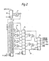
- Figures 2 and 3 show a decoder for decoding the data encoded in this form.
- the encoded data is fed to the serial data input of a four-stage shift register 20 which is clocked by a clock signal K having a frequency of 42 Megahertz, i.e. 14 times the data rate of the input data.
- the shift register 20 thus samples the input data every 23.8 nanoseconds, so that a series of binary ones is shifted into the shift register while the input signal is high, and a series of binary zeros is shifted in while the input signal is low.
- the purpose of the first two stages of the shift register 20 is to "de-boggle" the input data, i.e. to ensure that the data is fully synchronised to the clock K.
- FIG. 1 shows pulses in the signal NEQ corresponding to the transitions in the encoded data input signal DATAIN. It should be noted that each of these pulses is delayed by four clock beats with respect to the corresponding transition in the data input signal, as a result of the four-beat delay in the shift register 20.
- the signal NEQ is fed to the serial data input of another shift register 22, having twenty stages S1-S20.
- This shift register is clocked by the same clock signal K.
- Each transition in the input data causes a binary "1" to be injected into the first stage S1, and this is then shifted through the other stages S2-S20.
- the contents of the shift register 22 represent the transitions in a 476 nanosecond portion of the input data signal.
- the register is therefore long enough to hold a complete bit cell (333.3 nanoseconds) of the data signal, with an allowance for jitter.
- the outputs of selected stages of the shift register 22 are fed to a logic network consisting of OR gates 23, a register 24, OR gates 25 and a register 26 connected as shown.
- the registers 24 and 26 are both clocked by the signal K so that they are loaded at each clock beat.
- the outputs of register 26 provide signals STROBE, MID and END, and their inverses.
- STROBE is produced whenever a binary "1" occurs in stage S1 of the shift register 22, and is taken to indicate a transition at the trailing edge of a bit cell.
- MID is derived from a funnel of OR gates 23,25 connected to the outputs of stages S5-S11 of the shift register, and hence MID is produced whenever a binary "1" occurs anywhere in this range of stages. MID therefore indicates a transition at the ideal mid-point to the data cell, or at any of a range of positions on either side of this ideal position.
- END is derived from a funnel of OR gates 23,25 connected to the outputs of stages S12-S18 of the shift register, so that END is produced whenever a binary "1" occurs anywhere in this range of stages. END therefore indicates a transition at the ideal leading edge of the bit cell or at any of a range of positions on either side.
- a bit cell representing a Manchester-encoded "1" therefore causes STROBE, MID and END all to be true simultaneously. This condition is detected by an AND gate 30 ( Figure 3), producing a signal ONE. Similarly, a bit cell representing a Manchester-encoded "0" causes STROBE and END to be true while MID is false. This condition is detected by an AND gate 31, producing a signal ZERO.
- the signals ONE and ZERO are loaded into a register 32 at the next beat of clock K, and then transferred to another register 33 at the next again clock beat, where they control the set and reset inputs of an SR-type flip-flop 34.
- the output of this flip-flop is a signal DATAOUT which represents the decoded data signal in non-return-to-zero form.
- the outputs of the register 32 representing the signals ONE and ZERO delayed by one clock beat, are combined in an OR gate 36 and the result is loaded into register 33 at the next clock beat to produce a signal PLOAD.
- This signal indicates that a Manchester-encoded data cell representing either "0" or "1" has been decoded.
- PLOAD is fed to a control input P of the register 22, switching it from its shift mode into its parallel load mode. This causes the register 22 to be loaded, in parallel at the next clock beat.
- zeros are loaded into stages S6-S20. This clears the remnants of the data bit cell that has just been decoded.
- the outputs of stages S1-S4 are loaded into stages S2-S5, and NEQ is loaded into S1. This causes the bit representing the transition at the trailing edge of the bit cell to be shifted one stage down the register. This trailing edge bit is not cleared because it is also part of the next bit cell to be decoded.
- PLOAD is also fed to reset inputs R of the registers 24, 26 and 32, so as to clear them in preparation for the reception of the next Manchester-encoded bit cell.
- the logic network described above consists of four separate logic stages (OR gates 23, OR gates 25, AND gates 30,31 and OR gate 36) each of which has its output clocked into a register 24,26, 32,33.
- the operation of these four logic stages is pipelined, since they act simultaneously on data from four successive states of the shift register.
- the ability to pipeline the logic in this way is important, since it allows a relatively fast clock K to be used; i.e. the period of the clock K can be considerably shorter than the total delay through the logic network.
- the decoder described above is capable of correctly decoding Manchester-encoded data with jitter variations of up to 2 clock beats (47.6 nanoseconds) in either direction, allowing a further one clock beat in either direction for synchronisation errors in the de-boggle stages of shift register 20.
- different degrees of jitter cover can be obtained by changing the clock frequency and varying the number of stages in the shift register 22 and the connections of the OR gate funnels.
- the clock frequency is n times the input data rate
- the ideal positions for detecting the leading edge, mid-point, and trailing edge transitions will be in stages n+1, n/2+1 and 1 of the shift register.
- OR gate funnels connected to n/2+1 stages of the shift register, to allow transitions to be detected n/4 clock beats on either side of the ideal positions. Allowing for a possible error of one clock beat in either direction from synchronisation errors in the deboggle stages of shift register 20, this means that the decoder can handle jitter of up to n/4-1 clock beats in either direction.
- the decoder described above can also be modified by using a different clock signal, faster than the clock K, to clock the input shift register 20. This reduces the de-boggle errors.
- VLSI very-large-scale integrated
Abstract
Description
- This invention relates to a decoder for data encoded by a self-clocking code. The invention is particularly although not exclusively concerned with a decoder for Manchester encoded data.
- In a self-clocking code, data is encoded in such a way that the encoded signal contains both data and clock information, so that it is not necessary to transmit a separate clock signal. For example, in one form of Manchester code, referred to as Manchester bi-frequency code, the data is encoded as a succession of bit cells, with a transition at the boundary between each adjacent pair of cells. Bit cells representing zero contain no further transitions while those representing one contain a further transition at the mid point.
- Signals transmitted over a transmission line generally suffer from jitter, i.e. variations in the arrival time of the signals as a result of variations in the transmission characteristics of the line. Such jitter creates problems in decoding self-clocking codes. One known solution to this problem is to use a phase-locked loop for locking on to the incoming data so as to eliminate the jitter. However, phase-locked loops are complex and expensive.
- The object of the present invention is to provide a way of decoding self-clocking codes in the presence of jitter without using a phase-locked loop.
- According to the invention there is provided a decoder for decoding data in a self-clocking code, comprising:
- (a) a shift register,
- (b) means for clocking the shift register at a frequency equal to a multiple of the bit rate of the encoded data,
- (c) means for injecting a bit into the shift register to represent each transition in the encoded data, and
- (d) a logic network for detecting in the shift register a plurality of bits representing the transitions in a bit cell of the encoded data, the logic network being arranged to detect at least one of these bits in any one of a range of stages of the shift register, so as to allow for variations in the timing of the transitions as a result of jitter.
- One decoder in accordance with the invention will now be described by way of example with reference to the accompanying drawings.
- Figure 1 shows a Manchester bi-frequency encoded data signal, and also the waveforms of other signals in the decoder.
- Figures 2 and 3 are a logic circuit diagram of the decoder.
- Figure 1 shows one form of self-clocking code, referred to as a Manchester bi-frequency code. The encoded signal consists of a succession of bit cells, representing the binary digits "0" and "1". There is a transition in the signal level from high to low or vice versa at the boundary between each adjacent pair of bit cells. A cell representing a "1" has an additional transition at its mid point, while a cell representing "0" has no additional transition. In this example, it is assumed that the data rate of the input data is 3 million bits per second, so that each bit cell is 333.3 nanoseconds in duration.
- Figures 2 and 3 show a decoder for decoding the data encoded in this form.
- Referring to Figure 2, the encoded data is fed to the serial data input of a four-
stage shift register 20 which is clocked by a clock signal K having a frequency of 42 Megahertz, i.e. 14 times the data rate of the input data. The shift register 20 thus samples the input data every 23.8 nanoseconds, so that a series of binary ones is shifted into the shift register while the input signal is high, and a series of binary zeros is shifted in while the input signal is low. - The purpose of the first two stages of the
shift register 20 is to "de-boggle" the input data, i.e. to ensure that the data is fully synchronised to the clock K. - The outputs of the last two stages of the
shift register 20 are fed to the inputs of anon-equivalence gate 21, to produce a signal NEQ whenever a transition occurs in the input data. For example, Figure 1 shows pulses in the signal NEQ corresponding to the transitions in the encoded data input signal DATAIN. It should be noted that each of these pulses is delayed by four clock beats with respect to the corresponding transition in the data input signal, as a result of the four-beat delay in theshift register 20. - The signal NEQ is fed to the serial data input of another
shift register 22, having twenty stages S1-S20. This shift register is clocked by the same clock signal K. Each transition in the input data causes a binary "1" to be injected into the first stage S1, and this is then shifted through the other stages S2-S20. Thus, at any given time, the contents of theshift register 22 represent the transitions in a 476 nanosecond portion of the input data signal. The register is therefore long enough to hold a complete bit cell (333.3 nanoseconds) of the data signal, with an allowance for jitter. - For an ideal signal with no jitter, when the bit representing the transition at the trailing edge of a bit cell is in stage S1, the bit representing the transition at the leading edge of the cell will be in stage S15 and the bit representing the transition (if any) at the mid-point of the cell will be in stage S8. However, because of jitter and sampling errors in the de-boggle stages of
shift register 20, the actual positions of these transitions may vary by one or more stages from the ideal positions. - The outputs of selected stages of the
shift register 22 are fed to a logic network consisting ofOR gates 23, aregister 24, ORgates 25 and aregister 26 connected as shown. Theregisters register 26 provide signals STROBE, MID and END, and their inverses. - STROBE is produced whenever a binary "1" occurs in stage S1 of the
shift register 22, and is taken to indicate a transition at the trailing edge of a bit cell. - MID is derived from a funnel of
OR gates - Similarly, END is derived from a funnel of
OR gates - A bit cell representing a Manchester-encoded "1" therefore causes STROBE, MID and END all to be true simultaneously. This condition is detected by an AND gate 30 (Figure 3), producing a signal ONE. Similarly, a bit cell representing a Manchester-encoded "0" causes STROBE and END to be true while MID is false. This condition is detected by an
AND gate 31, producing a signal ZERO. - The signals ONE and ZERO are loaded into a
register 32 at the next beat of clock K, and then transferred to anotherregister 33 at the next again clock beat, where they control the set and reset inputs of an SR-type flip-flop 34. The output of this flip-flop is a signal DATAOUT which represents the decoded data signal in non-return-to-zero form. - It can be seen that, because MID and END are derived from funnels of OR gates each connected to a range of stages of the
shift register 22, the data will be correctly decoded even in the presence of jitter causing the transitions to deviate from their ideal positions. - Referring again to Figure 3, if STROBE and MID are both false while END is true, another AND
gate 35 is enabled, producing a signal START/STOP. This indicates either a start signal in the input data (represented by a bit cell containing only a single transition) or the end of a sequence of data bits. - Also as shown in Figure 3, the outputs of the
register 32, representing the signals ONE and ZERO delayed by one clock beat, are combined in anOR gate 36 and the result is loaded intoregister 33 at the next clock beat to produce a signal PLOAD. This signal indicates that a Manchester-encoded data cell representing either "0" or "1" has been decoded. - As shown in Figure 2, PLOAD is fed to a control input P of the
register 22, switching it from its shift mode into its parallel load mode. This causes theregister 22 to be loaded, in parallel at the next clock beat. As can be seen from Figure 2, zeros are loaded into stages S6-S20. This clears the remnants of the data bit cell that has just been decoded. At the same time, the outputs of stages S1-S4 are loaded into stages S2-S5, and NEQ is loaded into S1. This causes the bit representing the transition at the trailing edge of the bit cell to be shifted one stage down the register. This trailing edge bit is not cleared because it is also part of the next bit cell to be decoded. - PLOAD is also fed to reset inputs R of the
registers - It should be noted that the logic network described above consists of four separate logic stages (OR
gates 23, ORgates 25, ANDgates register - The decoder described above is capable of correctly decoding Manchester-encoded data with jitter variations of up to 2 clock beats (47.6 nanoseconds) in either direction, allowing a further one clock beat in either direction for synchronisation errors in the de-boggle stages of
shift register 20. - In other decoders in accordance with the invention, different degrees of jitter cover can be obtained by changing the clock frequency and varying the number of stages in the
shift register 22 and the connections of the OR gate funnels. In general, if the clock frequency is n times the input data rate, then the ideal positions for detecting the leading edge, mid-point, and trailing edge transitions will be in stages n+1, n/2+1 and 1 of the shift register. It is therefore possible to use OR gate funnels connected to n/2+1 stages of the shift register, to allow transitions to be detected n/4 clock beats on either side of the ideal positions. Allowing for a possible error of one clock beat in either direction from synchronisation errors in the deboggle stages ofshift register 20, this means that the decoder can handle jitter of up to n/4-1 clock beats in either direction. - The decoder described above can also be modified by using a different clock signal, faster than the clock K, to clock the
input shift register 20. This reduces the de-boggle errors. - The decoder described above can readily be implemented as a very-large-scale integrated (VLSI) circuit.
Claims (9)
Applications Claiming Priority (2)
| Application Number | Priority Date | Filing Date | Title |
|---|---|---|---|
| GB868606028A GB8606028D0 (en) | 1986-03-12 | 1986-03-12 | Decoder |
| GB8606028 | 1986-03-12 |
Publications (3)
| Publication Number | Publication Date |
|---|---|
| EP0237238A2 true EP0237238A2 (en) | 1987-09-16 |
| EP0237238A3 EP0237238A3 (en) | 1990-02-07 |
| EP0237238B1 EP0237238B1 (en) | 1992-06-17 |
Family
ID=10594413
Family Applications (1)
| Application Number | Title | Priority Date | Filing Date |
|---|---|---|---|
| EP87301701A Expired - Lifetime EP0237238B1 (en) | 1986-03-12 | 1987-02-26 | Decoder |
Country Status (6)
| Country | Link |
|---|---|
| US (1) | US4745626A (en) |
| EP (1) | EP0237238B1 (en) |
| AU (1) | AU584498B2 (en) |
| DE (1) | DE3779780T2 (en) |
| GB (1) | GB8606028D0 (en) |
| ZA (1) | ZA871566B (en) |
Cited By (4)
| Publication number | Priority date | Publication date | Assignee | Title |
|---|---|---|---|---|
| WO1994011952A1 (en) * | 1992-11-13 | 1994-05-26 | Ampex Systems Corporation | Pseudo clock extractor |
| EP0604189A2 (en) * | 1992-12-23 | 1994-06-29 | Honeywell Inc. | A bit-serial decoder for a specially encoded bit stream |
| US6021162A (en) * | 1997-10-01 | 2000-02-01 | Rosemount Inc. | Vortex serial communications |
| US6351489B1 (en) | 1996-09-30 | 2002-02-26 | Rosemount Inc. | Data bus communication technique for field instrument |
Families Citing this family (9)
| Publication number | Priority date | Publication date | Assignee | Title |
|---|---|---|---|---|
| DE3741758A1 (en) * | 1987-12-09 | 1989-06-29 | Messerschmitt Boelkow Blohm | SAILING YACHT |
| US4868569A (en) * | 1987-12-15 | 1989-09-19 | Schlumberger Well Services | Biphase digital look-ahead demodulating method and apparatus |
| US5023891A (en) | 1989-07-25 | 1991-06-11 | Sf2 Corporation | Method and circuit for decoding a Manchester code signal |
| US5056114A (en) * | 1989-08-03 | 1991-10-08 | Northern Telecom Limited | Method and apparatus for decoding Manchester encoded data |
| US5172395A (en) * | 1989-08-22 | 1992-12-15 | Cincinnati Electronics Corporation | Method of and apparatus for deriving an indication of noise content of data bits |
| US5313496A (en) * | 1990-12-26 | 1994-05-17 | Trw Inc. | Digital demodulator circuit |
| US5287359A (en) * | 1991-04-08 | 1994-02-15 | Digital Equipment Corporation | Synchronous decoder for self-clocking signals |
| US5748123A (en) * | 1995-12-20 | 1998-05-05 | Lg Semicon Co., Ltd. | Decoding apparatus for Manchester code |
| US5889820A (en) * | 1996-10-08 | 1999-03-30 | Analog Devices, Inc. | SPDIF-AES/EBU digital audio data recovery |
Citations (6)
| Publication number | Priority date | Publication date | Assignee | Title |
|---|---|---|---|---|
| US3764989A (en) * | 1972-12-20 | 1973-10-09 | Ultronic Systems Inc | Data sampling apparatus |
| GB2050122A (en) * | 1979-05-14 | 1980-12-31 | Honeywell Inf Systems | Data recovery system |
| EP0062945A1 (en) * | 1981-04-14 | 1982-10-20 | Koninklijke Philips Electronics N.V. | Device for interrogating and correcting a serial data signal |
| DE3235429A1 (en) * | 1982-09-24 | 1984-03-29 | Siemens AG, 1000 Berlin und 8000 München | Circuit arrangement for demodulating binary data signals |
| US4472686A (en) * | 1980-10-13 | 1984-09-18 | Hitachi, Ltd. | Circuit for reproducing and demodulating modulated digital signals |
| JPS62164272A (en) * | 1986-01-16 | 1987-07-20 | Hitachi Ltd | Data discriminating circuit |
Family Cites Families (4)
| Publication number | Priority date | Publication date | Assignee | Title |
|---|---|---|---|---|
| US4525848A (en) * | 1983-06-02 | 1985-06-25 | Prutec Limited | Manchester decoder |
| US4542420A (en) * | 1984-01-24 | 1985-09-17 | Honeywell Inc. | Manchester decoder |
| US4637037A (en) * | 1984-08-29 | 1987-01-13 | At&T Teletype Corporation | Biphase signal receiver |
| US4608702A (en) * | 1984-12-21 | 1986-08-26 | Advanced Micro Devices, Inc. | Method for digital clock recovery from Manchester-encoded signals |
-
1986
- 1986-03-12 GB GB868606028A patent/GB8606028D0/en active Pending
-
1987
- 1987-02-26 DE DE8787301701T patent/DE3779780T2/en not_active Expired - Fee Related
- 1987-02-26 EP EP87301701A patent/EP0237238B1/en not_active Expired - Lifetime
- 1987-03-04 US US07/021,914 patent/US4745626A/en not_active Expired - Fee Related
- 1987-03-04 ZA ZA871566A patent/ZA871566B/en unknown
- 1987-03-11 AU AU69897/87A patent/AU584498B2/en not_active Ceased
Patent Citations (6)
| Publication number | Priority date | Publication date | Assignee | Title |
|---|---|---|---|---|
| US3764989A (en) * | 1972-12-20 | 1973-10-09 | Ultronic Systems Inc | Data sampling apparatus |
| GB2050122A (en) * | 1979-05-14 | 1980-12-31 | Honeywell Inf Systems | Data recovery system |
| US4472686A (en) * | 1980-10-13 | 1984-09-18 | Hitachi, Ltd. | Circuit for reproducing and demodulating modulated digital signals |
| EP0062945A1 (en) * | 1981-04-14 | 1982-10-20 | Koninklijke Philips Electronics N.V. | Device for interrogating and correcting a serial data signal |
| DE3235429A1 (en) * | 1982-09-24 | 1984-03-29 | Siemens AG, 1000 Berlin und 8000 München | Circuit arrangement for demodulating binary data signals |
| JPS62164272A (en) * | 1986-01-16 | 1987-07-20 | Hitachi Ltd | Data discriminating circuit |
Non-Patent Citations (3)
| Title |
|---|
| IBM TECHNICAL DISCLOSURE BULLETIN, vol. 16, no. 10, March 1974, pages 3338-3339, New York, US; G.A. GEORGE: "Serial data clock control" * |
| P. Bylanski, D.G.W. Ingram, "Digital Transmission Systems", Revised edition 1980, Peter Perigrinus Ltd., Stevenage, GB, page 253. * |
| PATENT ABSTRACTS OF JAPAN, vol. 12, no. 2 (P-652)[2849], 7th January 1988; & JP-A-62 164 272 (HITACHI LTD) 20-07-1987 * |
Cited By (5)
| Publication number | Priority date | Publication date | Assignee | Title |
|---|---|---|---|---|
| WO1994011952A1 (en) * | 1992-11-13 | 1994-05-26 | Ampex Systems Corporation | Pseudo clock extractor |
| EP0604189A2 (en) * | 1992-12-23 | 1994-06-29 | Honeywell Inc. | A bit-serial decoder for a specially encoded bit stream |
| EP0604189A3 (en) * | 1992-12-23 | 1995-05-17 | Honeywell Inc | A bit-serial decoder for a specially encoded bit stream. |
| US6351489B1 (en) | 1996-09-30 | 2002-02-26 | Rosemount Inc. | Data bus communication technique for field instrument |
| US6021162A (en) * | 1997-10-01 | 2000-02-01 | Rosemount Inc. | Vortex serial communications |
Also Published As
| Publication number | Publication date |
|---|---|
| US4745626A (en) | 1988-05-17 |
| ZA871566B (en) | 1987-08-24 |
| EP0237238A3 (en) | 1990-02-07 |
| DE3779780T2 (en) | 1993-01-14 |
| DE3779780D1 (en) | 1992-07-23 |
| GB8606028D0 (en) | 1986-04-16 |
| AU6989787A (en) | 1987-09-17 |
| EP0237238B1 (en) | 1992-06-17 |
| AU584498B2 (en) | 1989-05-25 |
Similar Documents
| Publication | Publication Date | Title |
|---|---|---|
| EP0688447B1 (en) | De-skewer for serial data bus | |
| AU634124B2 (en) | Method and circuit for decoding a manchester code signal | |
| US4745626A (en) | Decoder | |
| US5359630A (en) | Method and apparatus for realignment of synchronous data | |
| JPS63126340A (en) | Decoder | |
| WO1994022248A1 (en) | Determination of optimal clock signal for sampling a packet | |
| JP3433426B2 (en) | Method and apparatus for decoding Manchester encoded data | |
| US4756010A (en) | Asynchronous/synchronous data receiver circuit | |
| US4686676A (en) | Apparatus and method for determining true data in a digital data stream from distorted data | |
| US6977973B1 (en) | System and method for decoding manchester data | |
| JPS63296425A (en) | Communication system | |
| US5748123A (en) | Decoding apparatus for Manchester code | |
| US5327466A (en) | 1X asynchronous data sampling clock | |
| US7079577B2 (en) | Wide window decoder circuit for dual phase pulse modulation | |
| US20060098770A1 (en) | Synchronizer for passing data from a first system to a second system | |
| US5510786A (en) | CMI encoder circuit | |
| US6367027B1 (en) | Skew pointer generation | |
| US4809301A (en) | Detection apparatus for bi-phase signals | |
| US5148450A (en) | Digital phase-locked loop | |
| NL8302446A (en) | DEVICE FOR DETECTING ERRORS IN A DIGITAL DATA FLOW CODED IN A DOUBLE DENSITY CODE. | |
| CN100581202C (en) | Dual phase pulse modulation decoder circuit | |
| JPS642306B2 (en) | ||
| JPS61289741A (en) | Consecutive protection circuit | |
| KR100214473B1 (en) | Menchester decoder | |
| US6470459B1 (en) | Half-word synchronization method for internal clock |
Legal Events
| Date | Code | Title | Description |
|---|---|---|---|
| PUAI | Public reference made under article 153(3) epc to a published international application that has entered the european phase |
Free format text: ORIGINAL CODE: 0009012 |
|
| AK | Designated contracting states |
Kind code of ref document: A2 Designated state(s): DE FR GB IT NL |
|
| PUAL | Search report despatched |
Free format text: ORIGINAL CODE: 0009013 |
|
| AK | Designated contracting states |
Kind code of ref document: A3 Designated state(s): DE FR GB IT NL |
|
| 17P | Request for examination filed |
Effective date: 19900110 |
|
| 17Q | First examination report despatched |
Effective date: 19910624 |
|
| ITF | It: translation for a ep patent filed |
Owner name: BARZANO' E ZANARDO ROMA S.P.A. |
|
| ITTA | It: last paid annual fee | ||
| GRAA | (expected) grant |
Free format text: ORIGINAL CODE: 0009210 |
|
| AK | Designated contracting states |
Kind code of ref document: B1 Designated state(s): DE FR GB IT NL |
|
| REF | Corresponds to: |
Ref document number: 3779780 Country of ref document: DE Date of ref document: 19920723 |
|
| ET | Fr: translation filed | ||
| PLBE | No opposition filed within time limit |
Free format text: ORIGINAL CODE: 0009261 |
|
| STAA | Information on the status of an ep patent application or granted ep patent |
Free format text: STATUS: NO OPPOSITION FILED WITHIN TIME LIMIT |
|
| 26N | No opposition filed | ||
| PGFP | Annual fee paid to national office [announced via postgrant information from national office to epo] |
Ref country code: NL Payment date: 19980127 Year of fee payment: 12 |
|
| PG25 | Lapsed in a contracting state [announced via postgrant information from national office to epo] |
Ref country code: NL Free format text: LAPSE BECAUSE OF NON-PAYMENT OF DUE FEES Effective date: 19990901 |
|
| REG | Reference to a national code |
Ref country code: GB Ref legal event code: IF02 |
|
| PGFP | Annual fee paid to national office [announced via postgrant information from national office to epo] |
Ref country code: FR Payment date: 20020114 Year of fee payment: 16 |
|
| PGFP | Annual fee paid to national office [announced via postgrant information from national office to epo] |
Ref country code: DE Payment date: 20020121 Year of fee payment: 16 |
|
| PG25 | Lapsed in a contracting state [announced via postgrant information from national office to epo] |
Ref country code: DE Free format text: LAPSE BECAUSE OF NON-PAYMENT OF DUE FEES Effective date: 20030902 |
|
| PG25 | Lapsed in a contracting state [announced via postgrant information from national office to epo] |
Ref country code: FR Free format text: LAPSE BECAUSE OF NON-PAYMENT OF DUE FEES Effective date: 20031031 |
|
| REG | Reference to a national code |
Ref country code: FR Ref legal event code: ST |
|
| PGFP | Annual fee paid to national office [announced via postgrant information from national office to epo] |
Ref country code: GB Payment date: 20040105 Year of fee payment: 18 |
|
| PG25 | Lapsed in a contracting state [announced via postgrant information from national office to epo] |
Ref country code: IT Free format text: LAPSE BECAUSE OF NON-PAYMENT OF DUE FEES;WARNING: LAPSES OF ITALIAN PATENTS WITH EFFECTIVE DATE BEFORE 2007 MAY HAVE OCCURRED AT ANY TIME BEFORE 2007. THE CORRECT EFFECTIVE DATE MAY BE DIFFERENT FROM THE ONE RECORDED. Effective date: 20050226 Ref country code: GB Free format text: LAPSE BECAUSE OF NON-PAYMENT OF DUE FEES Effective date: 20050226 |
|
| GBPC | Gb: european patent ceased through non-payment of renewal fee |
Effective date: 20050226 |