EP0230960A2 - Microcomputer having a highspeed operation mode and a low-speed operation mode - Google Patents
Microcomputer having a highspeed operation mode and a low-speed operation mode Download PDFInfo
- Publication number
- EP0230960A2 EP0230960A2 EP87100701A EP87100701A EP0230960A2 EP 0230960 A2 EP0230960 A2 EP 0230960A2 EP 87100701 A EP87100701 A EP 87100701A EP 87100701 A EP87100701 A EP 87100701A EP 0230960 A2 EP0230960 A2 EP 0230960A2
- Authority
- EP
- European Patent Office
- Prior art keywords
- operation mode
- speed operation
- sense amplifier
- enable signal
- low
- Prior art date
- Legal status (The legal status is an assumption and is not a legal conclusion. Google has not performed a legal analysis and makes no representation as to the accuracy of the status listed.)
- Granted
Links
Images


Classifications
-
- G—PHYSICS
- G06—COMPUTING; CALCULATING OR COUNTING
- G06F—ELECTRIC DIGITAL DATA PROCESSING
- G06F1/00—Details not covered by groups G06F3/00 - G06F13/00 and G06F21/00
- G06F1/26—Power supply means, e.g. regulation thereof
- G06F1/32—Means for saving power
- G06F1/3203—Power management, i.e. event-based initiation of a power-saving mode
- G06F1/3234—Power saving characterised by the action undertaken
- G06F1/324—Power saving characterised by the action undertaken by lowering clock frequency
-
- G—PHYSICS
- G06—COMPUTING; CALCULATING OR COUNTING
- G06F—ELECTRIC DIGITAL DATA PROCESSING
- G06F1/00—Details not covered by groups G06F3/00 - G06F13/00 and G06F21/00
- G06F1/26—Power supply means, e.g. regulation thereof
- G06F1/32—Means for saving power
- G06F1/3203—Power management, i.e. event-based initiation of a power-saving mode
-
- Y—GENERAL TAGGING OF NEW TECHNOLOGICAL DEVELOPMENTS; GENERAL TAGGING OF CROSS-SECTIONAL TECHNOLOGIES SPANNING OVER SEVERAL SECTIONS OF THE IPC; TECHNICAL SUBJECTS COVERED BY FORMER USPC CROSS-REFERENCE ART COLLECTIONS [XRACs] AND DIGESTS
- Y02—TECHNOLOGIES OR APPLICATIONS FOR MITIGATION OR ADAPTATION AGAINST CLIMATE CHANGE
- Y02D—CLIMATE CHANGE MITIGATION TECHNOLOGIES IN INFORMATION AND COMMUNICATION TECHNOLOGIES [ICT], I.E. INFORMATION AND COMMUNICATION TECHNOLOGIES AIMING AT THE REDUCTION OF THEIR OWN ENERGY USE
- Y02D10/00—Energy efficient computing, e.g. low power processors, power management or thermal management
Definitions
- the present invention relates to a microcomputer having a high-speed operation mode and a low-speed operation mode, and particularly to a microcomputer having a high-speed sense amplifier to read an instruction out of an instruction memory.
- a high frequency oscillator is used to apply a high frequency clock to a microcomputer in the high-speed operation mode, while a low frequency oscillator is used in the low-speed operation mode.
- a high-speed sense amplifier such as a current mirror type sense amplifier, will be required as a memory reading circuit. Since the sense amplifier of this type is driven by a large amount of current, a large amount of power is consumed. In the high-speed operation mode, an instruction reading cycle becomes short because the instruction execution speed is increased and because the high frequency clock is used.
- an instruction reading period can not be shortened less than a period that will be determined by characteristics of the sense amplifier and a memory to make sure an instruction fetch into a central processing unit (CPU).
- CPU central processing unit
- It is an object of the present invention is to provide a microcomputer having a high-speed operation mode and a low-speed operation mode with a low power consumption.
- It is another object of the present invention is to provide a microcomputer having a high-speed sense amplifier which can be activated with a low power in a low-speed operation mode.
- a microcomputer of the present invention has a sense amplifier and a circuit coupled to the sense amplifier to generate an enable signal to activate the sense amplifier and to apply the enable signal to the sense amplifier.
- the circuit generates a first enable signal which activates the sense amplifier in full time or with a large duty rate during a high-speed operation mode, and generates a second enable signal with a short duty rate during a low-speed operation mode.
- the first and second enable signals are selectively generated according to a mode designating signal.
- Fig. 1 illustrates a block diagram of a memory 106 and a reading circuit 107 in a microcomputer.
- Each of instruction cycles of the microcomputer consists of 01, 02, 03 and 04 states.
- An instruction in a read only memory (ROM) 106 is read thereof in the 04 state of a previous instruction cycle and the 01 state of a succeeding instruction cycle and is executed in the 02 to 04 state in the above succeeding instruction cycle.
- the reading circuit has a high-speed sense amplifier 107.
- An enable signal 104 is used in the present invention to activate the sense amplifier 107.
- the enable signal 104 is generated from an enable signal generating circuit 103 which receives a mode designating signal 101 and a reading control signal 102.
- the mode designating signal becomes "H° under a high-speed operation mode and becomes “L” under a low-speed operation mode.
- the reading control signal 102 becomes “H” in the 04 and 01 states and becomes “L” in the 02 and 03 states.
- Each of the states 01 to 04 is determined by one cycle of a clock applied to the microcomputer.
- the mode designating signal 101 becomes "H".
- An address 105 is applied to the ROM 106 from the 02 state in a previous cycle until the 01 state in a succeeding cycle according to an instruction prefetch architecture.
- the enable signal 104 is always "H * in spite of the reading control signal 102. Consequently, the sense amplifier 107 is always activated, so that an instruction 108 designated by the corresponding address 105 is read out of the ROM 106 via the sense amplifier 107. Since the enable signal 104 is fixed at "H" during the high-speed operation mode, each of instructions corresponding to addresses is sequentially read out of the ROM 106 and is sent to an instruction decoder in a CPU (not shown).
- the mode designating signal 101 becomes "L"
- the reading control signal 102 is applied to the sense amplifier 107 as the enable signal 104. Consequently, the sense amplifier 107 is activated only the 04 and 01 states through the address 105 is applied to the ROM in the 02 to 01 states. Since the high-speed sense amplifier 107 is used, an instruction is surely read out of the ROM 106 in the short period of time (04 and 01). According to this embodiment, power consumption of the sense amplifier 107 can be avoided in the 02 and 03 states of each cycle in the low-speed operation mode.
- Fig. 4 is a block diagram of another embodiment of the present invention.
- two divider circuit 410 and 411 are provided and have a different dividing ratio with each other.
- the divider circuit 410 receives a low-frequency clock 0L and applies a divided clock 402 to a enable signal generating circuit 403. While, the divider circuit 411 receives a high-frequency clock 0H and applies a divided clock 409 to the generating circuit 403.
- the mode designating signal 101 selects either one of the divided clocks 402 and 409. When the mode designating signal 101 is "H”, the divided clock 409 is selected and is applied to the sense amplifier 107 as the enable signal 104. On the other hand, when the mode designating signal 101 is "L", the divided clock 402 is applied to the sense amplifier 107 as the enable signal 104.
- the high-frequency clock 0H is divided into the clock 409 with a large duty rate, while the low-frequency clock 0L is divided into the clock 402 with a short duty rate. Therefore, the sense amplifier 107 is activated with the large duty rate in the high-speed operation mode and is activated with the short duty rate in the low-speed operation mode.
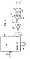
- Fig. 5 is a circuit diagram of the ROM 106 and the sense amplifier 107 according to the preferred embodiment of the present invention. It should be noted that only one bit line and the corresponding sense amplifier is illustrated.
- a bit line of the ROM 106 contains cells programmed according to an instruction code. Each cell is turned on by the corresponding word signal.
- the ROM 106 further contains a dummy line having dummy cells equal to the word signals in number. The dummy cells are always turned on by V DD voltage.
- the sense amplifier 107 has a current mirror type sense amplifiers SA1 connected to the bit line and SA2 connected to the dummy line.
- These sense amplifiers SA1 and SA2 consists of a complementally MOS circuit with a P channel MOS FET (P-FET) and an N channel MOS FET (N-FET).
- the sense amplifier SA1 has five N-FETs Q 1 , Q 2 , Qs, Q 7 and Q 8 and five P-FETS Qs, Q 4 , Q 6 , Q 9 and Qio.
- the sense amplifier SA2 has five N-FETs Q'i, Q' 2 , Q' 5 , Q' 7 and Q' 8 and five P-FETs Q' 3 , Q' 4 , Q' 6 , Q' 9 and Q'io.
- the enable signal 104 is applied to gates of Q 1 , Q'i, Q4 4 and Q' 4 .
- the inverted enable signal 104' is applied to gates of Q'a, Q 10 and Q' 10 .
- Q 1 , Q' 1 , Q 4 , Q' 4 , Qio, O' 10 and Q7 are provided to activate the sense amplifiers SA1 and SA2 by the enable signal 104.
- the sense amplifier SA2 is used as a reference voltage generating circuit, and the dummy line and dummy cells are used as a dummy current source.
- N-FET Q' 2 acts as an inverter.
- a potential at a node N 2 is equal to a threshold voltage of the N-FET Q' 2 , so that a current i is frown to the dummy line.
- the same current i is frown to the P-FET Q' 6 .
- the current mirror type sense amplifier is driven by a current mode and requires no precharge time, so that it can drive an ROM output (instruction) at high speed.
- the enable signal 104 is used to reduce the power consumption of the sense amplifier.
- the enable signal 104 is generated by a generating circuit shown in Fig. 6.
- "H” is set in a mode register 84 in the high-speed operation mode, while “L” is set therein in the low-speed operation mode.
- the mode designating signal 101 is outputted from the mode register 84 and is transferred to an NOR gate 64 via three latch circuits 83, 68 and 67. These latch circuits are provided to control an application timing to the NOR gate 64. That is, the mode designating signal 101 is latched into the first latch circuit 83 in the 04 state which is assigned to a write operation of the mode designating signal 101 an is latched into the second latch circuit 68 in the 02 state.
- This latch circuit 68 is used to protect a noise which arrives at the write operation.
- First and third flip-flops F1 and F2 consists of two AND gates (70, 71 and 78, 79) and two NOR gates (72, 73 and 80, 81), respectively.
- the second flip-flop F2 consists of two OR gates 74, 75 and two NAND gates 76 and 77.
- the low-frequency clock 0L (32 KHz) is applied to the AND gate 71 and the clock inverted by an inverter 69 is applied to the AND gate 70.
- the high-frequency ciock 0H (4 MHz) is applied to the AND gates 70, 71, 78, 79 and the OR gates 74, 75 in common, when the high-frequency oscillator is connected to the microcomputer.
- the timing signal 85 synchronized with a failing edge of each clock is applied to the third latch circuit 67 via an NOR gate 82.
- the mode designating signal 101' is applied to the NOR gate 64 in synchronous with the timing signal 85.
- the NOR gate 64 and an NOR gate 65 are connected with each other in accordance with a flip-flop manner. This flip-flop is set by either the mode designating signal 101' or an output of an NOR gate 66.
- the NOR gate 66 receives the low-frequency ctock 0L (32 kHz) and 0 4 signal and the read control signal 102 which is activated from a falling edge of the 0L clock in the 04 state till a rising edge of 01 signal.
- the mode designating signal 101' is "H", and therefore the flip-flop is set regardless of the read control signal 102 and outputs "L" signal to an NOR gate 62.
- the enable signal 104 becomes “L” (active lebel) because the output "H” of the NOR gate 62 is inverted by an inverter 63.
- the P-FETs Q 4 and Q' 4 are turned on, so that both the N-FETs Q 5 and Q' 5 are turned on to couple the bit line and the dummy line to the sense amplifiers SA1 and SA2, respectively.
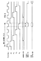
- the sense amplifier 107 is always activated in the high-speed operation mode as shown in Fig. 7.
- the mode designating signal 101' becomes "L".
- the flip-flop (64 and 65) is set only when the 0L and 04 are both "L” and is reset by 01 signal shown in Fig. 8. Therefore, the sense amplifier 107 is activated only when the 0L and
- each of state signals 01 to 04 is produced on a basis of the clock and is used to control timing of one machine (instruction) cycle.
- an instruction is read out of the ROM in a period T and is fetched into a CPU in 01 state.
- the CPU executes the fetched instruction in the 02 to 04 states.
- a next instruction is read out of the ROM according to an instruction prefetch architecture.
Abstract
Description
- The present invention relates to a microcomputer having a high-speed operation mode and a low-speed operation mode, and particularly to a microcomputer having a high-speed sense amplifier to read an instruction out of an instruction memory.
- In general, a high frequency oscillator is used to apply a high frequency clock to a microcomputer in the high-speed operation mode, while a low frequency oscillator is used in the low-speed operation mode. (n order to increase an operation speed of a microcomputer, not only an instruction execution speed but also an instruction reading speed must be increased. To increase the instruction reading speed, a high-speed sense amplifier, such as a current mirror type sense amplifier, will be required as a memory reading circuit. Since the sense amplifier of this type is driven by a large amount of current, a large amount of power is consumed. In the high-speed operation mode, an instruction reading cycle becomes short because the instruction execution speed is increased and because the high frequency clock is used. However, an instruction reading period can not be shortened less than a period that will be determined by characteristics of the sense amplifier and a memory to make sure an instruction fetch into a central processing unit (CPU). Thus, it will be required in the high-speed operation mode to use such a sense amplifier that is activated in a full time or with a large duty rate.
- On the other hand, when the low frequency oscillator is connected to the microcomputer in the low-speed operation mode, a low power consumption is required. In this case, a low frequency clock is applied to the microcomputer. However, a large amount of power is consumed by the above sense amplifier because it is activated with the same duty rate as that in the high-speed operation mode. To avoid the power consumption of the sense amplifier a low-power sense amplifier is required. However, since a microcomputer having the low-power sense amplifier has to be newly developed, a long development term and a design change are necessary.
- It is an object of the present invention is to provide a microcomputer having a high-speed operation mode and a low-speed operation mode with a low power consumption.
- It is another object of the present invention is to provide a microcomputer having a high-speed sense amplifier which can be activated with a low power in a low-speed operation mode.
- A microcomputer of the present invention has a sense amplifier and a circuit coupled to the sense amplifier to generate an enable signal to activate the sense amplifier and to apply the enable signal to the sense amplifier. The circuit generates a first enable signal which activates the sense amplifier in full time or with a large duty rate during a high-speed operation mode, and generates a second enable signal with a short duty rate during a low-speed operation mode. The first and second enable signals are selectively generated according to a mode designating signal.
-
- Fig. 1 illustrates a block diagram of one embodiment of the present invention;
- Fig. 2 illustrates a timing chart of Fig. 1 in a high-speed operation mode.
- Fig. 3 illustrates a timing chart of Fig. 1 in a low-speed operation mode;
- Fig. 4 illustrates a block diagram of another embodiment of the present invention;
- Fig. 5 illustrates a circuit diagram of a sense amplifier used in the present invention;
- Fig. 6 illustrates a circuit diagram of an enable signal generating circuit used in the present invention;
- Fig. 7 illustrates a timing chart of the sense amplifier shown in Fig. 5 in a high-speed operation mode; and
- Fig. 8 illustrates a timing chart of the sense amplifier shown in Fig. 5 in a low-speed operation mode.
- A detailed description of the present invention will be given by the reference of the accompanied drawings.
- Fig. 1 illustrates a block diagram of a
memory 106 and areading circuit 107 in a microcomputer. Each of instruction cycles of the microcomputer consists of 01, 02, 03 and 04 states. An instruction in a read only memory (ROM) 106 is read thereof in the 04 state of a previous instruction cycle and the 01 state of a succeeding instruction cycle and is executed in the 02 to 04 state in the above succeeding instruction cycle. The reading circuit has a high-speed sense amplifier 107. An enablesignal 104 is used in the present invention to activate thesense amplifier 107. The enablesignal 104 is generated from an enable signal generatingcircuit 103 which receives amode designating signal 101 and areading control signal 102. The mode designating signal becomes "H° under a high-speed operation mode and becomes "L" under a low-speed operation mode. Thereading control signal 102 becomes "H" in the 04 and 01 states and becomes "L" in the 02 and 03 states. Each of thestates 01 to 04 is determined by one cycle of a clock applied to the microcomputer. - In the high-speed operation mode shown in Fig. 2, the
mode designating signal 101 becomes "H". Anaddress 105 is applied to theROM 106 from the 02 state in a previous cycle until the 01 state in a succeeding cycle according to an instruction prefetch architecture. In this mode the enablesignal 104 is always "H* in spite of thereading control signal 102. Consequently, thesense amplifier 107 is always activated, so that aninstruction 108 designated by thecorresponding address 105 is read out of theROM 106 via thesense amplifier 107. Since the enablesignal 104 is fixed at "H" during the high-speed operation mode, each of instructions corresponding to addresses is sequentially read out of theROM 106 and is sent to an instruction decoder in a CPU (not shown). - On the other hand, in the low-speed operation mode, a low-frequency clock is applied to the microcomputer, and therefore a period of each state is enlarged as shown in Fig. 3. In this mode, the
mode designating signal 101 becomes "L", so that thereading control signal 102 is applied to thesense amplifier 107 as the enablesignal 104. Consequently, thesense amplifier 107 is activated only the 04 and 01 states through theaddress 105 is applied to the ROM in the 02 to 01 states. Since the high-speed sense amplifier 107 is used, an instruction is surely read out of theROM 106 in the short period of time (04 and 01). According to this embodiment, power consumption of thesense amplifier 107 can be avoided in the 02 and 03 states of each cycle in the low-speed operation mode. - Fig. 4 is a block diagram of another embodiment of the present invention. In this embodiment two
divider circuit 410 and 411 are provided and have a different dividing ratio with each other. Thedivider circuit 410 receives a low-frequency clock 0L and applies a dividedclock 402 to a enable signal generatingcircuit 403. While, the divider circuit 411 receives a high-frequency clock 0H and applies a dividedclock 409 to the generatingcircuit 403. Themode designating signal 101 selects either one of the dividedclocks mode designating signal 101 is "H", thedivided clock 409 is selected and is applied to thesense amplifier 107 as the enablesignal 104. On the other hand, when themode designating signal 101 is "L", thedivided clock 402 is applied to thesense amplifier 107 as the enablesignal 104. - According to this embodiment, the high-frequency clock 0H is divided into the
clock 409 with a large duty rate, while the low-frequency clock 0L is divided into theclock 402 with a short duty rate. Therefore, thesense amplifier 107 is activated with the large duty rate in the high-speed operation mode and is activated with the short duty rate in the low-speed operation mode. - Fig. 5 is a circuit diagram of the
ROM 106 and thesense amplifier 107 according to the preferred embodiment of the present invention. It should be noted that only one bit line and the corresponding sense amplifier is illustrated. A bit line of theROM 106 contains cells programmed according to an instruction code. Each cell is turned on by the corresponding word signal. TheROM 106 further contains a dummy line having dummy cells equal to the word signals in number. The dummy cells are always turned on by VDD voltage. Thesense amplifier 107 has a current mirror type sense amplifiers SA1 connected to the bit line and SA2 connected to the dummy line. These sense amplifiers SA1 and SA2 consists of a complementally MOS circuit with a P channel MOS FET (P-FET) and an N channel MOS FET (N-FET). The sense amplifier SA1 has five N-FETs Q1, Q2, Qs, Q7 and Q8 and five P-FETS Qs, Q4, Q6, Q9 and Qio. The sense amplifier SA2 has five N-FETs Q'i, Q'2, Q'5, Q'7 and Q'8 and five P-FETs Q'3, Q'4, Q'6, Q'9 and Q'io. The enablesignal 104 is applied to gates of Q1, Q'i, Q44 and Q'4. The inverted enable signal 104' is applied to gates of Q'a, Q10 and Q'10. Q1, Q'1, Q4, Q'4, Qio, O'10 and Q7 are provided to activate the sense amplifiers SA1 and SA2 by theenable signal 104. In this embodiment, the sense amplifier SA2 is used as a reference voltage generating circuit, and the dummy line and dummy cells are used as a dummy current source. - Since a source of N-FET Q'5 and a gate of N-FET Q'2 is connected to an output of the dummy line, the N-FET Q'2 acts as an inverter. As a result, a potential at a node N2 is equal to a threshold voltage of the N-FET Q'2, so that a current i is frown to the dummy line. At this state the same current i is frown to the P-FET Q'6. Since the P-FET Q'6 and P-FET Q'g are a current mirror circuit, a current i' (i' = gm of Q'g/gm of Q'6 x i) is frown to the P-FET Q'9 and is further frown to the N-FETs Q'8 and Q'7. Further, since the N-FET Q8 whose gate is applied an output of the SA2 and the N-FET Q'8 are a current mirror circuit, a current i" (i" gm of Qa/gm of Q'8 x i') is frown to the N-FET Q8.
- At this time, when all cells of the bit line are turned on, the current i is frown to the bit line. It should be noted that gm of Q6 is equal to that of Q'6 and that gm of Qg is equal to that of Q'9. As a result, the current i' is frown to the P-FET Q9, and therefore a voltage of a node N1 becomes "H". Since the node N1 is connected to a gate of a C MOS inverter circuit Q11 and Q12, the N-FET Q11 is turned on. Thus, an output "H" is derived from the
ROM 106. - On the other hand, if at least one of cells on the bit line is turned off, the current i is not frown to the N-FET Q5, and therefore the P-FET Q6 is turned off. Consequently, the node N1 become "L (Vss)", and the P-FET Q12 is turned on. Thus, an output "L" is derived from the
ROM 106. - As described above, the current mirror type sense amplifier is driven by a current mode and requires no precharge time, so that it can drive an ROM output (instruction) at high speed. However, a large amount of current is required. In the present invention, the enable signal 104 is used to reduce the power consumption of the sense amplifier.
- The enable
signal 104 is generated by a generating circuit shown in Fig. 6. In this embodiment, "H" is set in amode register 84 in the high-speed operation mode, while "L" is set therein in the low-speed operation mode. Themode designating signal 101 is outputted from themode register 84 and is transferred to an NORgate 64 via threelatch circuits gate 64. That is, themode designating signal 101 is latched into thefirst latch circuit 83 in the 04 state which is assigned to a write operation of the mode designating signal 101 an is latched into thesecond latch circuit 68 in the 02 state. Thislatch circuit 68 is used to protect a noise which arrives at the write operation. Thereafter themode designating signal 101 is latched into thethird latch circuit 67 which controls a timing when the low-frequency clock 0L is changed to the high-frequency clock 0H, and vice versa. The timing is determined by three cascaded flip-flops F1 to F3. First and third flip-flops F1 and F2 consists of two AND gates (70, 71 and 78, 79) and two NOR gates (72, 73 and 80, 81), respectively. The second flip-flop F2 consists of two ORgates NAND gates gate 71 and the clock inverted by aninverter 69 is applied to the ANDgate 70. While the high-frequency ciock 0H (4 MHz) is applied to the ANDgates OR gates timing signal 85 synchronized with a failing edge of each clock is applied to thethird latch circuit 67 via an NORgate 82. The mode designating signal 101' is applied to the NORgate 64 in synchronous with thetiming signal 85. The NORgate 64 and an NORgate 65 are connected with each other in accordance with a flip-flop manner. This flip-flop is set by either the mode designating signal 101' or an output of an NORgate 66. The NORgate 66 receives the low-frequency ctock 0L (32 kHz) and 0 4 signal and the read control signal 102 which is activated from a falling edge of the 0L clock in the 04 state till a rising edge of 01 signal. - In the high-speed operation mode, the mode designating signal 101' is "H", and therefore the flip-flop is set regardless of the read
control signal 102 and outputs "L" signal to an NORgate 62. If a stop signal (STOP) and a halt signal (HALT) which are generated when a operation of the microcomputer should be stopped are not present, the enable signal 104 becomes "L" (active lebel) because the output "H" of the NORgate 62 is inverted by aninverter 63. In response to the enablesignal 104, the P-FETs Q4 and Q'4 are turned on, so that both the N-FETs Q5 and Q'5 are turned on to couple the bit line and the dummy line to the sense amplifiers SA1 and SA2, respectively. Thus, thesense amplifier 107 is always activated in the high-speed operation mode as shown in Fig. 7. - On the other hand, when the low-speed operation mode is required, the mode designating signal 101' becomes "L". As a result, the flip-flop (64 and 65) is set only when the 0L and 04 are both "L" and is reset by 01 signal shown in Fig. 8. Therefore, the
sense amplifier 107 is activated only when the 0L and - 4 are both "L". In the remaining period, the enable signal 104 becomes "H", and therefore, the N-FETs 01 and Q'i are turned on while the P-FETs Q4 and Q'4 are turned off. Thus, the N-FETs Q5 and Q'5 are both turned off. Consequently, the P-FETs Q6 and Q'6 are discoupled from the bit line and the dummy line, respectively. At this period, no power is consumed because a current path is cut off.
- In Figs. 7 and 8, each of state signals 01 to 04 is produced on a basis of the clock and is used to control timing of one machine (instruction) cycle. In the low-speec operation of the embodiment, an instruction is read out of the ROM in a period T and is fetched into a CPU in 01 state. The CPU executes the fetched instruction in the 02 to 04 states. Further, in the 04 state, a next instruction is read out of the ROM according to an instruction prefetch architecture.
- Turning to Fig. 6, when either the stop signal or the halt signal becomes "H", the enable signal 104 becomes "H", and therefore, the
sense amplifier 107 is inactivated.
Claims (6)
Applications Claiming Priority (2)
| Application Number | Priority Date | Filing Date | Title |
|---|---|---|---|
| JP10419/86 | 1986-01-20 | ||
| JP1041986 | 1986-01-20 |
Publications (3)
| Publication Number | Publication Date |
|---|---|
| EP0230960A2 true EP0230960A2 (en) | 1987-08-05 |
| EP0230960A3 EP0230960A3 (en) | 1988-04-20 |
| EP0230960B1 EP0230960B1 (en) | 1992-05-13 |
Family
ID=11749626
Family Applications (1)
| Application Number | Title | Priority Date | Filing Date |
|---|---|---|---|
| EP87100701A Expired - Lifetime EP0230960B1 (en) | 1986-01-20 | 1987-01-20 | Microcomputer having a highspeed operation mode and a low-speed operation mode |
Country Status (4)
| Country | Link |
|---|---|
| US (2) | US4862348A (en) |
| EP (1) | EP0230960B1 (en) |
| JP (1) | JPH0715674B2 (en) |
| DE (1) | DE3778920D1 (en) |
Cited By (2)
| Publication number | Priority date | Publication date | Assignee | Title |
|---|---|---|---|---|
| EP0379178A2 (en) * | 1989-01-17 | 1990-07-25 | Sanyo Electric Co., Ltd. | Computer memory controller power saving management |
| EP0580338A1 (en) * | 1992-07-21 | 1994-01-26 | Advanced Micro Devices, Inc. | External memory access control for a processing system |
Families Citing this family (24)
| Publication number | Priority date | Publication date | Assignee | Title |
|---|---|---|---|---|
| US5483659A (en) * | 1987-09-14 | 1996-01-09 | Yamamura; Kimio | Apparatus for controlling a signal processing system to operate in high and low speed modes |
| JP2749819B2 (en) * | 1987-10-26 | 1998-05-13 | 松下電工株式会社 | Shared memory control method |
| US5255193A (en) * | 1988-05-12 | 1993-10-19 | Nissan Motor Company | Traction control system for controlling engine output and brake for maintaining optimum wheel traction with road friction level dependent brake control |
| US5113511A (en) * | 1989-06-02 | 1992-05-12 | Atari Corporation | System for dynamically providing predicted high/slow speed accessing memory to a processing unit based on instructions |
| US5222239A (en) * | 1989-07-28 | 1993-06-22 | Prof. Michael H. Davis | Process and apparatus for reducing power usage microprocessor devices operating from stored energy sources |
| JPH04356799A (en) * | 1990-08-29 | 1992-12-10 | Mitsubishi Electric Corp | Semiconductor memory |
| JPH05189976A (en) * | 1991-09-03 | 1993-07-30 | Seiko Epson Corp | Semiconductor device and electronic equipment |
| GB2297398B (en) * | 1995-01-17 | 1999-11-24 | Advanced Risc Mach Ltd | Accessing cache memories |
| US5530384A (en) * | 1995-04-27 | 1996-06-25 | Xilinx, Inc. | Sense amplifier having selectable power and speed modes |
| JP2718399B2 (en) * | 1995-08-10 | 1998-02-25 | 日本電気株式会社 | Data radio for computer connection |
| US5778428A (en) * | 1995-12-22 | 1998-07-07 | International Business Machines Corporation | Programmable high performance mode for multi-way associative cache/memory designs |
| JPH10275140A (en) * | 1997-03-31 | 1998-10-13 | Nec Ic Microcomput Syst Ltd | Microcomputer |
| US7000065B2 (en) * | 2002-01-02 | 2006-02-14 | Intel Corporation | Method and apparatus for reducing power consumption in a memory bus interface by selectively disabling and enabling sense amplifiers |
| US7216240B2 (en) * | 2002-12-11 | 2007-05-08 | Intel Corporation | Apparatus and method for address bus power control |
| US7152167B2 (en) * | 2002-12-11 | 2006-12-19 | Intel Corporation | Apparatus and method for data bus power control |
| US20040128416A1 (en) * | 2002-12-11 | 2004-07-01 | Tsvika Kurts | Apparatus and method for address bus power control |
| US7529955B2 (en) * | 2005-06-30 | 2009-05-05 | Intel Corporation | Dynamic bus parking |
| JP4557179B2 (en) * | 2006-08-04 | 2010-10-06 | オムロン株式会社 | Microcomputer device |
| JP5266589B2 (en) * | 2009-05-14 | 2013-08-21 | ルネサスエレクトロニクス株式会社 | Nonvolatile semiconductor memory device |
| FR2947587A1 (en) | 2009-07-03 | 2011-01-07 | Total Sa | PROCESS FOR EXTRACTING HYDROCARBONS BY ELECTROMAGNETIC HEATING OF A SUBTERRANEAN FORMATION IN SITU |
| EP2539897B1 (en) * | 2010-02-23 | 2020-03-18 | Rambus Inc. | Methods and circuits for dynamically scaling dram power and performance |
| JP2015056198A (en) * | 2013-09-13 | 2015-03-23 | 株式会社東芝 | Memory chip, memory device, and reading-out method |
| JP5714149B2 (en) * | 2014-03-07 | 2015-05-07 | ルネサスエレクトロニクス株式会社 | Nonvolatile semiconductor memory device |
| CN104517645B (en) * | 2014-05-16 | 2019-08-13 | 上海华虹宏力半导体制造有限公司 | Flash memory low speed reading mode control circuit |
Citations (3)
| Publication number | Priority date | Publication date | Assignee | Title |
|---|---|---|---|---|
| US3941989A (en) * | 1974-12-13 | 1976-03-02 | Mos Technology, Inc. | Reducing power consumption in calculators |
| US4137563A (en) * | 1976-06-30 | 1979-01-30 | Canon Kabushiki Kaisha | Circuitry for reducing power dissipation in equipment which operates in synchronism with clock pulses |
| JPS58107930A (en) * | 1981-12-22 | 1983-06-27 | Fujitsu Ltd | Clock controlling system |
Family Cites Families (9)
| Publication number | Priority date | Publication date | Assignee | Title |
|---|---|---|---|---|
| JPS6019029B2 (en) * | 1978-03-29 | 1985-05-14 | ブリテイツシユ・ブロ−ドキヤステイング・コ−ポレ−シヨン | Digital data processing equipment |
| US4508101A (en) * | 1982-04-09 | 1985-04-02 | Monsanto Company | Thermal energy storage system |
| US4594657A (en) * | 1983-04-22 | 1986-06-10 | Motorola, Inc. | Semaphore for memory shared by two asynchronous microcomputers |
| EP0134822B1 (en) * | 1983-07-27 | 1988-07-20 | Ibm Deutschland Gmbh | Digital memory |
| JPS6079593A (en) * | 1983-10-07 | 1985-05-07 | Hitachi Ltd | Semiconductor integrated circuit system |
| JPS60175293A (en) * | 1984-02-21 | 1985-09-09 | Toshiba Corp | Semiconductor memory |
| US4727491A (en) * | 1984-06-27 | 1988-02-23 | Compaq Computer Corporation | Personal computer having normal and high speed execution modes |
| US4807194A (en) * | 1986-04-24 | 1989-02-21 | Matsushita Electric Industrial Co., Ltd. | Seimiconductor memory device having sub bit lines |
| US4807195A (en) * | 1987-05-18 | 1989-02-21 | International Business Machines Corporation | Apparatus and method for providing a dual sense amplifier with divided bit line isolation |
-
1987
- 1987-01-20 DE DE8787100701T patent/DE3778920D1/en not_active Expired - Lifetime
- 1987-01-20 US US07/004,927 patent/US4862348A/en not_active Expired - Lifetime
- 1987-01-20 JP JP1162087A patent/JPH0715674B2/en not_active Expired - Lifetime
- 1987-01-20 EP EP87100701A patent/EP0230960B1/en not_active Expired - Lifetime
-
1989
- 1989-01-18 US US07/298,436 patent/US4930067A/en not_active Expired - Lifetime
Patent Citations (3)
| Publication number | Priority date | Publication date | Assignee | Title |
|---|---|---|---|---|
| US3941989A (en) * | 1974-12-13 | 1976-03-02 | Mos Technology, Inc. | Reducing power consumption in calculators |
| US4137563A (en) * | 1976-06-30 | 1979-01-30 | Canon Kabushiki Kaisha | Circuitry for reducing power dissipation in equipment which operates in synchronism with clock pulses |
| JPS58107930A (en) * | 1981-12-22 | 1983-06-27 | Fujitsu Ltd | Clock controlling system |
Non-Patent Citations (2)
| Title |
|---|
| IBM TECHNICAL DISCLOSURE BULLETIN, vol. 24, no. 6, November 1981, pages 2773,2774, New York, US; S. BOWERS et al.: "Machine-cycle extension in a data processor" * |
| PATENT ABSTRACTS OF JAPAN, vol. 7, no. 212 (P-224)[1357], 20th September 1983; & JP-A-58 107 930 (FUJITSU K.K.) 27-06-1983 * |
Cited By (4)
| Publication number | Priority date | Publication date | Assignee | Title |
|---|---|---|---|---|
| EP0379178A2 (en) * | 1989-01-17 | 1990-07-25 | Sanyo Electric Co., Ltd. | Computer memory controller power saving management |
| EP0379178A3 (en) * | 1989-01-17 | 1992-02-19 | Sanyo Electric Co., Ltd. | Computer memory controller power saving management |
| EP0580338A1 (en) * | 1992-07-21 | 1994-01-26 | Advanced Micro Devices, Inc. | External memory access control for a processing system |
| US5408639A (en) * | 1992-07-21 | 1995-04-18 | Advanced Micro Devices | External memory access control for a processing system |
Also Published As
| Publication number | Publication date |
|---|---|
| US4862348A (en) | 1989-08-29 |
| JPH0715674B2 (en) | 1995-02-22 |
| EP0230960A3 (en) | 1988-04-20 |
| DE3778920D1 (en) | 1992-06-17 |
| JPS63238649A (en) | 1988-10-04 |
| US4930067A (en) | 1990-05-29 |
| EP0230960B1 (en) | 1992-05-13 |
Similar Documents
| Publication | Publication Date | Title |
|---|---|---|
| EP0230960A2 (en) | Microcomputer having a highspeed operation mode and a low-speed operation mode | |
| US5604705A (en) | Static random access memory sense amplifier | |
| US5546355A (en) | Integrated circuit memory having a self-timed write pulse independent of clock frequency and duty cycle | |
| KR960004567B1 (en) | Output buffer of semiconductor memory device | |
| JP3209485B2 (en) | Synchronous memory device with automatic precharge function | |
| JPH07177015A (en) | Power cut circuit for synchronous type semiconductor device | |
| KR0171942B1 (en) | Burst length detection circuit | |
| US6144614A (en) | Semiconductor integrated circuit having a clock and latch circuits for performing synchronous switching operations | |
| KR0137462B1 (en) | Dynamic random access memory | |
| US7154316B2 (en) | Circuit for controlling pulse width | |
| USRE36532E (en) | Synchronous semiconductor memory device having an auto-precharge function | |
| US6781919B2 (en) | Address selection circuit and semiconductor memory device with synchronous and asynchronous address signal paths | |
| EP0281867B1 (en) | Semiconductor memory device with address generator | |
| KR100263843B1 (en) | Semiconductor memory device | |
| US5600599A (en) | Data signal output circuit and semiconductor memory device including the same | |
| JP2908776B2 (en) | Write recovery guarantee circuit for memory device and operation signal control method | |
| KR0142405B1 (en) | Semiconductor memory device having pre-charge function | |
| KR100219491B1 (en) | Automatic precharge bank selection circuit | |
| KR980011454A (en) | Light control circuit | |
| EP0544370A2 (en) | Circuit structure having distributed registers with self-timed reading and writing operations | |
| JPH0458676B2 (en) | ||
| JPH09270190A (en) | Semiconductor memory | |
| JPH11185471A (en) | Internal clock signal generation circuit | |
| KR910000386B1 (en) | Semiconductor memory device with reset signal generating circuit | |
| KR20030000355A (en) | A write enable signal buffer for enabling high-speed write operation and a semiconductor memory device using this buffer |
Legal Events
| Date | Code | Title | Description |
|---|---|---|---|
| PUAI | Public reference made under article 153(3) epc to a published international application that has entered the european phase |
Free format text: ORIGINAL CODE: 0009012 |
|
| 17P | Request for examination filed |
Effective date: 19870120 |
|
| AK | Designated contracting states |
Kind code of ref document: A2 Designated state(s): DE FR GB |
|
| PUAL | Search report despatched |
Free format text: ORIGINAL CODE: 0009013 |
|
| AK | Designated contracting states |
Kind code of ref document: A3 Designated state(s): DE FR GB |
|
| 17Q | First examination report despatched |
Effective date: 19900521 |
|
| GRAA | (expected) grant |
Free format text: ORIGINAL CODE: 0009210 |
|
| AK | Designated contracting states |
Kind code of ref document: B1 Designated state(s): DE FR GB |
|
| REF | Corresponds to: |
Ref document number: 3778920 Country of ref document: DE Date of ref document: 19920617 |
|
| ET | Fr: translation filed | ||
| PLBE | No opposition filed within time limit |
Free format text: ORIGINAL CODE: 0009261 |
|
| STAA | Information on the status of an ep patent application or granted ep patent |
Free format text: STATUS: NO OPPOSITION FILED WITHIN TIME LIMIT |
|
| 26N | No opposition filed | ||
| REG | Reference to a national code |
Ref country code: GB Ref legal event code: IF02 |
|
| REG | Reference to a national code |
Ref country code: GB Ref legal event code: 732E |
|
| REG | Reference to a national code |
Ref country code: FR Ref legal event code: TP |
|
| PGFP | Annual fee paid to national office [announced via postgrant information from national office to epo] |
Ref country code: FR Payment date: 20060110 Year of fee payment: 20 |
|
| PGFP | Annual fee paid to national office [announced via postgrant information from national office to epo] |
Ref country code: DE Payment date: 20060112 Year of fee payment: 20 |
|
| PGFP | Annual fee paid to national office [announced via postgrant information from national office to epo] |
Ref country code: GB Payment date: 20060118 Year of fee payment: 20 |
|
| PG25 | Lapsed in a contracting state [announced via postgrant information from national office to epo] |
Ref country code: GB Free format text: LAPSE BECAUSE OF EXPIRATION OF PROTECTION Effective date: 20070119 |
|
| REG | Reference to a national code |
Ref country code: GB Ref legal event code: PE20 |