EP0224626B1 - Multi-signal processor synchronized system - Google Patents
Multi-signal processor synchronized system Download PDFInfo
- Publication number
- EP0224626B1 EP0224626B1 EP85430037A EP85430037A EP0224626B1 EP 0224626 B1 EP0224626 B1 EP 0224626B1 EP 85430037 A EP85430037 A EP 85430037A EP 85430037 A EP85430037 A EP 85430037A EP 0224626 B1 EP0224626 B1 EP 0224626B1
- Authority
- EP
- European Patent Office
- Prior art keywords
- signal
- processor
- signal processors
- bus
- signal processor
- Prior art date
- Legal status (The legal status is an assumption and is not a legal conclusion. Google has not performed a legal analysis and makes no representation as to the accuracy of the status listed.)
- Expired
Links
Images


Classifications
-
- G—PHYSICS
- G06—COMPUTING; CALCULATING OR COUNTING
- G06F—ELECTRIC DIGITAL DATA PROCESSING
- G06F9/00—Arrangements for program control, e.g. control units
- G06F9/06—Arrangements for program control, e.g. control units using stored programs, i.e. using an internal store of processing equipment to receive or retain programs
- G06F9/46—Multiprogramming arrangements
- G06F9/48—Program initiating; Program switching, e.g. by interrupt
- G06F9/4806—Task transfer initiation or dispatching
- G06F9/4812—Task transfer initiation or dispatching by interrupt, e.g. masked
- G06F9/4825—Interrupt from clock, e.g. time of day
-
- G—PHYSICS
- G06—COMPUTING; CALCULATING OR COUNTING
- G06F—ELECTRIC DIGITAL DATA PROCESSING
- G06F13/00—Interconnection of, or transfer of information or other signals between, memories, input/output devices or central processing units
- G06F13/14—Handling requests for interconnection or transfer
- G06F13/20—Handling requests for interconnection or transfer for access to input/output bus
- G06F13/22—Handling requests for interconnection or transfer for access to input/output bus using successive scanning, e.g. polling
-
- H—ELECTRICITY
- H04—ELECTRIC COMMUNICATION TECHNIQUE
- H04B—TRANSMISSION
- H04B1/00—Details of transmission systems, not covered by a single one of groups H04B3/00 - H04B13/00; Details of transmission systems not characterised by the medium used for transmission
- H04B1/66—Details of transmission systems, not covered by a single one of groups H04B3/00 - H04B13/00; Details of transmission systems not characterised by the medium used for transmission for reducing bandwidth of signals; for improving efficiency of transmission
- H04B1/667—Details of transmission systems, not covered by a single one of groups H04B3/00 - H04B13/00; Details of transmission systems not characterised by the medium used for transmission for reducing bandwidth of signals; for improving efficiency of transmission using a division in frequency subbands
-
- H—ELECTRICITY
- H04—ELECTRIC COMMUNICATION TECHNIQUE
- H04J—MULTIPLEX COMMUNICATION
- H04J3/00—Time-division multiplex systems
- H04J3/02—Details
- H04J3/06—Synchronising arrangements
- H04J3/062—Synchronisation of signals having the same nominal but fluctuating bit rates, e.g. using buffers
- H04J3/0626—Synchronisation of signals having the same nominal but fluctuating bit rates, e.g. using buffers plesiochronous multiplexing systems, e.g. plesiochronous digital hierarchy [PDH], jitter attenuators
-
- H—ELECTRICITY
- H04—ELECTRIC COMMUNICATION TECHNIQUE
- H04M—TELEPHONIC COMMUNICATION
- H04M1/00—Substation equipment, e.g. for use by subscribers
- H04M1/253—Telephone sets using digital voice transmission
Definitions
- a number of digital systems include specialized separate items devoted respectively either to signal processing, or to system's management.
- the signal processors require a fairly large computing power, while their memory capacities need not to be important.
- the requirements are all the way around.
- the above statements may be illustrated by way of an example, e.g. a digital voice and data transmission system.
- a number of local voice terminals are to be attached to a digital transmission network.
- Each voice signal needs to be processed. It is first converted into digital form prior to being transmitted over the network.
- the outgoing voice signal is submitted to more or less complex operations, made to get the best voice coding quality, e. g. in terms of quantizing noise for a given bit rate.
- the processing workload required is fairly high, but it mainly consists in repetitive computing operations on the same data.
- the voice signal is processed by segments each 20 ms long. Each voice segment is sampled at, say, 8 KHz, and thus provides a block of 160 samples. Each sample is coded in PCM with say 8 bits. Then each 20 ms, the whole block of PCM coded samples are reprocessed to lower the final number of bits required to code the same samples, while keeping the coding quality at the highest possible level.
- the Control Unit would have to control the coders VO operations, say, for transferring each 20 ms the bits deriving from a voice segment processed by each of the signal processors attached to the same Control Unit.
- a system architecture is proposed here, which conveniently combines hard and soft devices enabling program parametering of the system to adjust to the specific system configuration required.
- signal processor will thus be used in this application for this kind of processor, even if the executed task is not related to signal processing.
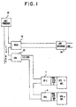
- FIG. 1 shows a block diagram illustrating the basic architecture of a system made according to this invention.
- Each one of a set of n Voice Terminal Units is attached through an interface (VTU1 INT) through (VTUn INT) to a device (A/D, D/A) performing analog-to-digital and digital-to-analog conversion respectively.
- VTU1 INT Voice Terminal Unit
- VTUn INT a device
- A/D digital-to-analog conversion
- the voice signal limited to the telephone frequency bandwidth 300-3400 Hz, is sampled at 8 KHz, and coded in PCM mlaw with 8 bits per sample.
- the voice signal is then considered by segments 20 ms long and each block of samples is recorded to improve the signal to noise ratio of the coded signal while keeping the bit rate required to a predetermined minimal level.
- This target may be reached by processing the PCM coded signal into a signal processor using BCPCM techniques combined with split band and dynamic allocation of coding resources, as disclosed in the above mentioned patent.
- BCPCM the 8-bit PCM coded samples are processed by blocks of samples wherefrom a characteristic term is derived (e.g. the largest sample) and then the samples of the block are requantized relative to the characteristic term.
- the voice signal is also split into several (p) subbands, which means that each original block provides p different blocks. The requantizing is performed within each subband with the requantizing number of bits being dynamically assigned to the subband.
- each signal processor provides a block of bits resulting from the coding of a voice segment 20 ms long.
- the Unit Processor 20 is made to manage the transfer of voice originating bits, and/or service bits, such as telephone signaling, to and from a line interface through a High Speed Communication Adapter (HSCA) 26.
- HSCA High Speed Communication Adapter
- the data exchanges between the Unit Processor 20 and the n individual Signal Processors is made on a time sharing basis as schematically represented in figure 2.
- the transfer between a given Signal Processor "i" and the Unit Processor, is made active during a time interval Di, and inactive during a time interval Pi. All the n Signal Processors should then be scanned within a time interval equal to the time involved in processing one block of samples within a Signal Processor, i.e. 20 ms.
- the synchronization of the system is achieved by a logic system which gives a "Start process” and a "Data exchange” order to the Unit Processor and to the n different Signal Processors.
- the data exchanges are performed through a single data exchange bus (DE Bus) on which contention is avoided due to the above mentioned time distribution.
- DE Bus data exchange bus
- the time slot Dn is equal to T/n.
- one may also choose to process the exchange more than one voice segment at a time. For instance assuming two voice segments should be packed together, then Dn 2T/n . And so on.
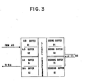
- a so called “ping- pong” technique is implemented as schematically represented in figure 3.
- the data transfers from and to the signal processor are performed through double-buffering means (R1 and R2).
- Each couple of buffers is made to operate in a ping-pong mode, which means, alternatively.
- the A/D Buffer Register R1 is being loaded with PCM coded samples
- the PCM coded samples to be recoded using BCPCM and compression techniques as disclosed in the above mentioned patent are fetched out of A/D Buffer Register R2 by the Signal processor.
- the system synchronization is achieved by the Signal Processor adapter (SPA) 22, normally and regularly requesting a Unit Processor interrupt every T/n second and also feeding clock signals to the signal processors SP1 - SPn to start its operation.
- SPA Signal Processor adapter
- each signal processor SP1 - SPn reads a byte (a sample) out of its corresponding A/D PCM converter and feeds it into one of its A/D buffers R1 or R2 alternatively.
- the Signal Processor reads a byte out of one of its D/A buffers R1 or R2 and feeds it into the D/A PCM converter.
- the conversion from A/D PCM to compressed coding is performed over a block of say 160 PCM coded samples representing a segment of voice signal 20 ms long.
- the cycle is started by a special interrupt to the Signal Processor.
- the system synchronization is achieved by SPA22 through use of a SYSTEM SYNCHRONIZATION REGISTER (SSR).
- SSR SYSTEM SYNCHRONIZATION REGISTER
- the System Synchronization Register of Figure 4 is a 8-bit counter which may be preset by program to define the maximum count cycle. In practice said counter is doubled for buffering purposes (see SSR write and SSR Read).
- the counter is divided into two parts.
- the four HIGH order bits will determine the ping-pong bit, which controls two consecutive signal processing cycles, and the start cycle flag, for each signal processor by raising the level of one out of eight outputs labeled SCF TO SP1 through SCF TO SP8 upon the decoding of the contents of bit positions 1-3 of SSR Read.
- the four low order bit positions are initialized by the Unit Processor to fit with the number of PCM coded samples processed by the Signal Processor.
- the input clock for this counter has been made to be a 500 microseconds clock the cycle of which corresponds to four PCM coded samples.
- a flexibility of the system may be achieved through the selection of the "p" value.
- the multiplication by four is made through hardware.
- the initial time of a total synchronization cycle is TO and if the SSR has been initialized to count p clock periods, the following table shows the details of the events occurring during the succeding synchronization cycle.
- the asterisk indicate an interrupt requested to the Unit Processor 22 (UP) through the carry bit of upper part of SSR Read (see. figure 4) section.
- the Start Cycle Flag (SCF) position indicates which signal processor starts a new signal processing cycle after transferring one block of samples to coding buffer and from decoding buffer R1 or R2 (depending upon the ping-pong P/P bit value).
- the above table indications show the read/write data exchange from/to Unit Processor and from/to a Signal Processor.
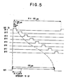
- the interrupts are synchronized as indicated in figure 5. All the signal processors will receive regularly the normal 125 microseconds interrupt. Indications are given to each Signal Processor through the contents of a status byte location in their Input/Output memory space. This space is made to store a start cycle flag SCF and a ping-pong bit. In fact, the start cycle flag will be up for a signal processor, 395 microseconds after the raising of the related interrupt to up. The start cycle flag SCF will be up for each signal processor, only once every N x 125 microseconds. This indication, together with the ping-pong bit value being at a one binary value, will start the initialization of a new signal processing cycle within the signal processor.
- the start cycle flag SCF timing chart is represented in figure 5, with an emphasized portion showing the relative phase of the 125 microseconds interrupt, with respect to the corresponding Start Cycle Flag.
- the SCF signal will automatically go down to zero level 105.4 microseconds after the interrupt request has been made to the corresponding signal processor SP.
- the SSR counting can be inhibited by setting a CONTROL REGISTER bit 0 to zero level and thus inhibit Unit Processor interrupts as well as start cycle flag generation.
Description
- A number of digital systems include specialized separate items devoted respectively either to signal processing, or to system's management. The signal processors require a fairly large computing power, while their memory capacities need not to be important. For system's managing devices, the requirements are all the way around.
- The above statements may be illustrated by way of an example, e.g. a digital voice and data transmission system. Assume a number of local voice terminals are to be attached to a digital transmission network. Each voice signal needs to be processed. It is first converted into digital form prior to being transmitted over the network. For that purpose the outgoing voice signal is submitted to more or less complex operations, made to get the best voice coding quality, e. g. in terms of quantizing noise for a given bit rate. The processing workload required is fairly high, but it mainly consists in repetitive computing operations on the same data. For instance, the voice signal is processed by segments each 20 ms long. Each voice segment is sampled at, say, 8 KHz, and thus provides a block of 160 samples. Each sample is coded in PCM with say 8 bits. Then each 20 ms, the whole block of PCM coded samples are reprocessed to lower the final number of bits required to code the same samples, while keeping the coding quality at the highest possible level.
- A number of coders have been proposed to perform the above coding operations. One may refer for instance to European Patent 0002998 (US patent 4,216,354) to the same assignee for further details on these coders. But, with any of these coders, the rate of input/output operations is fairly limited (e.g. one operation per 20 ms) and requires little data transfers when compared with the processing workload for the compression and related signal processing operations.
- One good reason for doing the compression operations has to deal with the price of transmission channels. Important savings are made by compressing voice signal to enable concentrating (e.g. multiplexing) as many voices as possible on the same transmission channel. Consequently several voice coders should be attached to the same channel, through a Control Unit made to manage the interface operations between a set of Voice terminals (coders) and a common channel.
- For the above cited example of coder, for instance, the Control Unit would have to control the coders VO operations, say, for transferring each 20 ms the bits deriving from a voice segment processed by each of the signal processors attached to the same Control Unit.
- These transfers could be made using different methods. Some of these methods would be fairly rigid, and not allow easy reconfiguration of the network in the field.
- A system architecture is proposed here, which conveniently combines hard and soft devices enabling program parametering of the system to adjust to the specific system configuration required.
- The same architecture not only applies to voice multiplexing.
- It may be used in all the machines where several processors execute Tasks which may be included in a fixed time frame.
- The expression "signal processor" will thus be used in this application for this kind of processor, even if the executed task is not related to signal processing.
- The above statements will be made apparent from the following description, made with reference to the attached figures.
-
- Figure 1 is a block diagram of a system incorporating the invention.
- Figure 2 represents a time diagram.
- Figure 3 is a block diagram for the invention.
- Figure 4 is a circuit for the invention.
- Figure 5 is a time diagram.
- Figure 1 shows a block diagram illustrating the basic architecture of a system made according to this invention. Each one of a set of n Voice Terminal Units is attached through an interface (VTU1 INT) through (VTUn INT) to a device (A/D, D/A) performing analog-to-digital and digital-to-analog conversion respectively. In the A/D for instance, the voice signal, limited to the telephone frequency bandwidth 300-3400 Hz, is sampled at 8 KHz, and coded in PCM mlaw with 8 bits per sample. The voice signal is then considered by
segments 20 ms long and each block of samples is recorded to improve the signal to noise ratio of the coded signal while keeping the bit rate required to a predetermined minimal level. This target may be reached by processing the PCM coded signal into a signal processor using BCPCM techniques combined with split band and dynamic allocation of coding resources, as disclosed in the above mentioned patent. According to the BCPCM technique, the 8-bit PCM coded samples are processed by blocks of samples wherefrom a characteristic term is derived (e.g. the largest sample) and then the samples of the block are requantized relative to the characteristic term. In addition, in the above mentioned patent, the voice signal is also split into several (p) subbands, which means that each original block provides p different blocks. The requantizing is performed within each subband with the requantizing number of bits being dynamically assigned to the subband. - At the end of this signal processing, each signal processor provides a block of bits resulting from the coding of a
voice segment 20 ms long. - Every 20 ms, then, the transfer of a block of bits should be made from each operating signal processor (1 through n) toward the
Unit Processor 20 and vice versa. These transfers are made through a Signal Processor Adapter (SPA) 22. - The
Unit Processor 20, is made to manage the transfer of voice originating bits, and/or service bits, such as telephone signaling, to and from a line interface through a High Speed Communication Adapter (HSCA) 26. - The data exchanges between the
Unit Processor 20 and the n individual Signal Processors is made on a time sharing basis as schematically represented in figure 2. - The transfer between a given Signal Processor "i" and the Unit Processor, is made active during a time interval Di, and inactive during a time interval Pi. All the n Signal Processors should then be scanned within a time interval equal to the time involved in processing one block of samples within a Signal Processor, i.e. 20 ms.
- The synchronization of the system is achieved by a logic system which gives a "Start process" and a "Data exchange" order to the Unit Processor and to the n different Signal Processors. The data exchanges are performed through a single data exchange bus (DE Bus) on which contention is avoided due to the above mentioned time distribution. Such a non-contention mode of operation, also enables simplifying both system hardware and software.
- In summary, once defined the number of Voice Terminal Units, for instance "n", to be served by a given Unit Processor, and once defined the voice segment time length T, then the time slot Dn is equal to T/n. In fact, one may also choose to process the exchange more than one voice segment at a time. For instance assuming two voice segments should be packed together, then Dn = 2T/n . And so on.
- Also, should the number of Voice Units or their operating cycles need to be adjusted in the field, then, the operator could adjust the system to the required Dn.
- In addition, to make the system operate even more smoothly, a so called "ping- pong" technique is implemented as schematically represented in figure 3. The data transfers from and to the signal processor are performed through double-buffering means (R1 and R2). Each couple of buffers is made to operate in a ping-pong mode, which means, alternatively. For instance, assume at a given time slot Di, the A/D Buffer Register R1 is being loaded with PCM coded samples, during the same time slot, the PCM coded samples to be recoded using BCPCM and compression techniques as disclosed in the above mentioned patent, are fetched out of A/D Buffer Register R2 by the Signal processor.
- The same operating process applies to the D/A Buffers and to the I/O means connected to the D.E. Bus, as well.
- The system synchronization is achieved by the Signal Processor adapter (SPA) 22, normally and regularly requesting a Unit Processor interrupt every T/n second and also feeding clock signals to the signal processors SP1 - SPn to start its operation.
- Assuming the Voice signal is first to be sampled at 8 KHz and coded in PCM with 8 bits per sample, then every 125 microsecond on an interrupt mode, each signal processor SP1 - SPn reads a byte (a sample) out of its corresponding A/D PCM converter and feeds it into one of its A/D buffers R1 or R2 alternatively. At the same time, the Signal Processor reads a byte out of one of its D/A buffers R1 or R2 and feeds it into the D/A PCM converter.
- The conversion from A/D PCM to compressed coding is performed over a block of say 160 PCM coded samples representing a segment of
voice signal 20 ms long. The cycle is started by a special interrupt to the Signal Processor. - Obviously, when the transfer from/to A/D and D/A buffers affects the ping (R1) buffers, then the compression/decompression is performed over pong (R2) buffers.
- In addition, assume n = 8, and each voice segments is T = 20 ms long, then T should be divided into n = 8 slots each 20/8 = 2,5 ms long, thus Di = 2,5 ms and Pi = 17,5 ms.
- The system synchronization is achieved by SPA22 through use of a SYSTEM SYNCHRONIZATION REGISTER (SSR). The System Synchronization Register of Figure 4 is a 8-bit counter which may be preset by program to define the maximum count cycle. In practice said counter is doubled for buffering purposes (see SSR write and SSR Read).
- The counter is divided into two parts. The four HIGH order bits will determine the ping-pong bit, which controls two consecutive signal processing cycles, and the start cycle flag, for each signal processor by raising the level of one out of eight outputs labeled SCF TO SP1 through SCF TO SP8 upon the decoding of the contents of bit positions 1-3 of SSR Read.
- The four low order bit positions are initialized by the Unit Processor to fit with the number of PCM coded samples processed by the Signal Processor. The input clock for this counter has been made to be a 500 microseconds clock the cycle of which corresponds to four PCM coded samples.
- If the counter is initialized by the Unit Processor to count "p" clock periods, then, the number of samples processed by each signal processor for analysis or compression and synthesis or decompression purposes will be: N = 4× p × 8 = 32 p
- A flexibility of the system may be achieved through the selection of the "p" value.
- The multiplication by four is made through hardware.
- If the initial time of a total synchronization cycle is TO and if the SSR has been initialized to count p clock periods, the following table shows the details of the events occurring during the succeding synchronization cycle.

- The asterisk indicate an interrupt requested to the Unit Processor 22 (UP) through the carry bit of upper part of SSR Read (see. figure 4) section. The Start Cycle Flag (SCF) position indicates which signal processor starts a new signal processing cycle after transferring one block of samples to coding buffer and from decoding buffer R1 or R2 (depending upon the ping-pong P/P bit value).
- In other words, the above table indications show the read/write data exchange from/to Unit Processor and from/to a Signal Processor.
- The interrupts are synchronized as indicated in figure 5. All the signal processors will receive regularly the normal 125 microseconds interrupt. Indications are given to each Signal Processor through the contents of a status byte location in their Input/Output memory space. This space is made to store a start cycle flag SCF and a ping-pong bit. In fact, the start cycle flag will be up for a signal processor, 395 microseconds after the raising of the related interrupt to up. The start cycle flag SCF will be up for each signal processor, only once every N x 125 microseconds. This indication, together with the ping-pong bit value being at a one binary value, will start the initialization of a new signal processing cycle within the signal processor. The start cycle flag SCF timing chart is represented in figure 5, with an emphasized portion showing the relative phase of the 125 microseconds interrupt, with respect to the corresponding Start Cycle Flag. The SCF signal will automatically go down to zero level 105.4 microseconds after the interrupt request has been made to the corresponding signal processor SP.
- In addition, the SSR counting can be inhibited by setting a CONTROL REGISTER bit 0 to zero level and thus inhibit Unit Processor interrupts as well as start cycle flag generation.
Claims (8)
said set of signal processors being connected to said Signal Processor Adapter through said D.E. Bus; said SPA including means for generating Unit Processor interrupt request on a cyclic basis, and means for sequentially scanning the set of signal processors to control data exchanges between said Unit Processor and each of said signal processors.
means for generating logic signals for sequentially scanning the set of signal processors, whereby data transfer operations to and from signal processors and the Unit Processor are being synchronized.
Priority Applications (4)
| Application Number | Priority Date | Filing Date | Title |
|---|---|---|---|
| DE8585430037T DE3575829D1 (en) | 1985-10-30 | 1985-10-30 | SYNCHRONIZED SYSTEM FOR SEVERAL SIGNAL PROCESSORS. |
| EP85430037A EP0224626B1 (en) | 1985-10-30 | 1985-10-30 | Multi-signal processor synchronized system |
| JP61214226A JPS62107598A (en) | 1985-10-30 | 1986-09-12 | Synchronization system |
| US06/917,945 US4845752A (en) | 1985-10-30 | 1986-10-14 | Multi-signal processor synchronized system |
Applications Claiming Priority (1)
| Application Number | Priority Date | Filing Date | Title |
|---|---|---|---|
| EP85430037A EP0224626B1 (en) | 1985-10-30 | 1985-10-30 | Multi-signal processor synchronized system |
Publications (2)
| Publication Number | Publication Date |
|---|---|
| EP0224626A1 EP0224626A1 (en) | 1987-06-10 |
| EP0224626B1 true EP0224626B1 (en) | 1990-01-31 |
Family
ID=8194584
Family Applications (1)
| Application Number | Title | Priority Date | Filing Date |
|---|---|---|---|
| EP85430037A Expired EP0224626B1 (en) | 1985-10-30 | 1985-10-30 | Multi-signal processor synchronized system |
Country Status (4)
| Country | Link |
|---|---|
| US (1) | US4845752A (en) |
| EP (1) | EP0224626B1 (en) |
| JP (1) | JPS62107598A (en) |
| DE (1) | DE3575829D1 (en) |
Cited By (1)
| Publication number | Priority date | Publication date | Assignee | Title |
|---|---|---|---|---|
| DE102008055134A1 (en) | 2008-12-23 | 2010-07-01 | Robert Bosch Gmbh | Electrical or electronic composite component and method for producing an electrical or electronic composite component |
Families Citing this family (10)
| Publication number | Priority date | Publication date | Assignee | Title |
|---|---|---|---|---|
| JP2755951B2 (en) * | 1988-01-30 | 1998-05-25 | キヤノン株式会社 | Information processing device |
| US5768613A (en) * | 1990-07-06 | 1998-06-16 | Advanced Micro Devices, Inc. | Computing apparatus configured for partitioned processing |
| US6230255B1 (en) | 1990-07-06 | 2001-05-08 | Advanced Micro Devices, Inc. | Communications processor for voice band telecommunications |
| JP2900719B2 (en) * | 1992-08-24 | 1999-06-02 | 日本電気株式会社 | Audio codec processing method |
| US5996018A (en) * | 1995-12-06 | 1999-11-30 | International Business Machines Corporation | Method and apparatus to reduce jitter and end-to-end delay for multimedia data signalling |
| EP1021045A1 (en) * | 1999-01-12 | 2000-07-19 | Deutsche Thomson-Brandt Gmbh | Method for processing and apparatus for encoding audio or video frame data |
| EP1020998B1 (en) * | 1999-01-12 | 2009-03-18 | Thomson Licensing | Method and apparatus for encoding audio frame data |
| EP1020997A3 (en) * | 1999-01-12 | 2001-01-31 | Deutsche Thomson-Brandt Gmbh | Method for processing and apparatus for encoding audio or video frame data |
| EP1021044A1 (en) * | 1999-01-12 | 2000-07-19 | Deutsche Thomson-Brandt Gmbh | Method and apparatus for encoding or decoding audio or video frame data |
| US6205509B1 (en) * | 1999-07-15 | 2001-03-20 | 3Com Corporation | Method for improving interrupt response time |
Family Cites Families (5)
| Publication number | Priority date | Publication date | Assignee | Title |
|---|---|---|---|---|
| FR2412987A1 (en) * | 1977-12-23 | 1979-07-20 | Ibm France | PROCESS FOR COMPRESSION OF DATA RELATING TO THE VOICE SIGNAL AND DEVICE IMPLEMENTING THIS PROCEDURE |
| US4475011A (en) * | 1977-12-27 | 1984-10-02 | Stromberg-Carlson Corporation | Arrangement of interactive telephone switching processors providing selective functional capability by port |
| US4445213A (en) * | 1979-07-31 | 1984-04-24 | Bell Telephone Laboratories, Incorporated | Communication line interface for controlling data information having differing transmission characteristics |
| DE3236812A1 (en) * | 1982-10-05 | 1984-04-05 | Standard Elektrik Lorenz Ag, 7000 Stuttgart | REMOTE CONTROL SYSTEM |
| US4567606A (en) * | 1982-11-03 | 1986-01-28 | International Telephone And Telegraph Corporation | Data processing apparatus and method for use in speech recognition |
-
1985
- 1985-10-30 EP EP85430037A patent/EP0224626B1/en not_active Expired
- 1985-10-30 DE DE8585430037T patent/DE3575829D1/en not_active Expired - Fee Related
-
1986
- 1986-09-12 JP JP61214226A patent/JPS62107598A/en active Granted
- 1986-10-14 US US06/917,945 patent/US4845752A/en not_active Expired - Fee Related
Cited By (1)
| Publication number | Priority date | Publication date | Assignee | Title |
|---|---|---|---|---|
| DE102008055134A1 (en) | 2008-12-23 | 2010-07-01 | Robert Bosch Gmbh | Electrical or electronic composite component and method for producing an electrical or electronic composite component |
Also Published As
| Publication number | Publication date |
|---|---|
| JPS62107598A (en) | 1987-05-18 |
| EP0224626A1 (en) | 1987-06-10 |
| JPH0225320B2 (en) | 1990-06-01 |
| US4845752A (en) | 1989-07-04 |
| DE3575829D1 (en) | 1990-03-08 |
Similar Documents
| Publication | Publication Date | Title |
|---|---|---|
| KR930010298B1 (en) | Telephone switching system adjunct call processing arrangement | |
| US4328543A (en) | Control architecture for a communications controller | |
| US4864566A (en) | Precise multiplexed transmission and reception of analog and digital data through a narrow-band channel | |
| US4330857A (en) | Dynamically variable priority, variable position channels in a TDMA burst | |
| US5570356A (en) | High bandwidth communications system having multiple serial links | |
| EP0224626B1 (en) | Multi-signal processor synchronized system | |
| US5631651A (en) | Telecom adapter for interfacing computing devices to the analog telephone network | |
| US4319353A (en) | Priority threaded message burst mechanism for TDMA communication | |
| US3790715A (en) | Digital transmission terminal for voice and low speed data | |
| US3997727A (en) | Time division multiplexed digital switching apparatus | |
| JPH04276930A (en) | Daisy chain multiplexer | |
| US4932024A (en) | System for automatic control of devices, apparata and peripheral units for signal switching and processing | |
| US4143246A (en) | Time division line interface circuit | |
| US5280532A (en) | N:1 bit compression apparatus and method | |
| US3711650A (en) | Adaptive pulse code modulation system | |
| US3971891A (en) | Adaptable time division switch | |
| US4307461A (en) | Call processor for a satellite communications controller | |
| JP3088306B2 (en) | Multi-channel integrated circuit and multi-channel data processing method | |
| US5193089A (en) | Key telephone system | |
| CA2052409C (en) | Sub-rate time switch | |
| KR0149898B1 (en) | Synchronization of multiple transmit/receive devices | |
| US6895016B1 (en) | Method and apparatus for interfacing multiple data channels to a bus | |
| EP0035231B1 (en) | Tdma satellite communications system | |
| US5099234A (en) | Switching matrix network for digital audio signals | |
| CA2216011A1 (en) | "adpcm transcoder" |
Legal Events
| Date | Code | Title | Description |
|---|---|---|---|
| PUAI | Public reference made under article 153(3) epc to a published international application that has entered the european phase |
Free format text: ORIGINAL CODE: 0009012 |
|
| AK | Designated contracting states |
Kind code of ref document: A1 Designated state(s): DE FR GB IT |
|
| 17P | Request for examination filed |
Effective date: 19870821 |
|
| 17Q | First examination report despatched |
Effective date: 19890404 |
|
| GRAA | (expected) grant |
Free format text: ORIGINAL CODE: 0009210 |
|
| AK | Designated contracting states |
Kind code of ref document: B1 Designated state(s): DE FR GB IT |
|
| REF | Corresponds to: |
Ref document number: 3575829 Country of ref document: DE Date of ref document: 19900308 |
|
| ET | Fr: translation filed | ||
| ITF | It: translation for a ep patent filed |
Owner name: IBM - DR. ALFREDO BRAVI |
|
| PLBE | No opposition filed within time limit |
Free format text: ORIGINAL CODE: 0009261 |
|
| STAA | Information on the status of an ep patent application or granted ep patent |
Free format text: STATUS: NO OPPOSITION FILED WITHIN TIME LIMIT |
|
| 26N | No opposition filed | ||
| ITTA | It: last paid annual fee | ||
| PGFP | Annual fee paid to national office [announced via postgrant information from national office to epo] |
Ref country code: GB Payment date: 19950926 Year of fee payment: 11 |
|
| PGFP | Annual fee paid to national office [announced via postgrant information from national office to epo] |
Ref country code: FR Payment date: 19951009 Year of fee payment: 11 |
|
| PGFP | Annual fee paid to national office [announced via postgrant information from national office to epo] |
Ref country code: DE Payment date: 19951030 Year of fee payment: 11 |
|
| PG25 | Lapsed in a contracting state [announced via postgrant information from national office to epo] |
Ref country code: GB Effective date: 19961030 |
|
| GBPC | Gb: european patent ceased through non-payment of renewal fee |
Effective date: 19961030 |
|
| PG25 | Lapsed in a contracting state [announced via postgrant information from national office to epo] |
Ref country code: FR Effective date: 19970630 |
|
| PG25 | Lapsed in a contracting state [announced via postgrant information from national office to epo] |
Ref country code: DE Effective date: 19970701 |
|
| REG | Reference to a national code |
Ref country code: FR Ref legal event code: ST |