EP0220059B1 - Appareil numérique de mise en forme d'enveloppe - Google Patents
Appareil numérique de mise en forme d'enveloppe Download PDFInfo
- Publication number
- EP0220059B1 EP0220059B1 EP86308005A EP86308005A EP0220059B1 EP 0220059 B1 EP0220059 B1 EP 0220059B1 EP 86308005 A EP86308005 A EP 86308005A EP 86308005 A EP86308005 A EP 86308005A EP 0220059 B1 EP0220059 B1 EP 0220059B1
- Authority
- EP
- European Patent Office
- Prior art keywords
- signal
- digital
- values
- gain control
- signals
- Prior art date
- Legal status (The legal status is an assumption and is not a legal conclusion. Google has not performed a legal analysis and makes no representation as to the accuracy of the status listed.)
- Expired - Lifetime
Links
Images


Classifications
-
- H—ELECTRICITY
- H04—ELECTRIC COMMUNICATION TECHNIQUE
- H04N—PICTORIAL COMMUNICATION, e.g. TELEVISION
- H04N5/00—Details of television systems
- H04N5/04—Synchronising
- H04N5/06—Generation of synchronising signals
- H04N5/067—Arrangements or circuits at the transmitter end
- H04N5/0675—Arrangements or circuits at the transmitter end for mixing the synchronising signals with the picture signal or mutually
Definitions
- the invention pertains to video signal processing devices for generating television synchronization signals for combining with the video signal being processed. More particularly, the invention relates to television synchronizing signal waveform generators in which the various synchronizing signals to be combined with the video signal are generated digitally.
- a television signal is a composite of several different signal components, generally, falling within one of two classes of signals, namely, a video information signal component and several synchronizing signal components.
- the common television signals are formed of lines of horizontally distributed video information separated by intervals of horizontal line related synchronizing signals defining the beginning of each line.
- the horizontal lines are further organized into rasters of vertically distributed lines defining fields of lines separated by vertical field related synchronizing signals.
- the fields are organized into frames, each composed of two interlaced fields of horizontal lines, with lines of each field having a different raster position upon display.
- the various synchronizing signals included in television signals serve to synchronize the processing of the television signals and the operation of the processing and other television signal utilization devices.
- the synchronizing signals include vertical and horizontal blanking intervals, each formed of a composite of several synchronizing signals.
- the vertical blanking interval includes a vertical blanking level extending between leading and trailing signal transition edges that determine the durations of the vertical blanking interval. Onto this blanking level is impressed a number of horizontal blanking intervals, a number of equalization pulses, a serrated pulse interval defining a vertical sync pulse, and a burst (typically 9 to ll cycles) of the sinusoidal chrominance subcarrier signal (color burst) following each horizontal sync pulse during about the latter one-half of the vertical interval.
- Each horizontal blanking interval during the latter one-half of the vertical blanking interval and the entire field of lines between consecutive vertical blanking intervals includes a horizontal blanking level extending between leading and trailing signal transition edges that determine the duration of the horizontal blanking interval. Impressed on each horizontal blanking level is a horizontal sync pulse followed by a color burst. One horizontal sync pulse and one color burst are provided for each horizontal line of the televison signal and serve to keep the horizontal scanning and color generation synchronized.
- the vertical sync pulse is provided for each field of the television signal to keep vertical scanning synchronized. The serrations of the vertical sync pulse prevent loss of horizontal scanning synchronization.
- Equalization pulses are provided to insure proper scanning motion synchronization with the required interlacing of the two fields that compose a television frame.
- the horizontal and vertical blanking levels serve to blank the display during horizontal and vertical retraces, with the associated transition edges effecting a smooth signal change between the video information signal intervals and the blanking intervals.
- Proper display and processing of television signals requires precise formation of the synchronizing signals and insertion of them within the television signal.
- the video information is usually generated separately from the synchronizing signals, with the two being added together, i.e., combined, in a multiplexer.
- new synchronizing signals are usually inserted in the processed television signals. This combining or insertion is performed at the conclusion of the generation or processing to avoid the introduction of timing disturbance to and the degradation of the synchronizing signals.
- transmission of television signals through communication channels often introduces such disturbance and degradation.
- a video tape recorder (VTR) is an example of such a communication channel. Following such transmission, new synchronizing signals are inserted in the television signal to restore it to its proper form.
- Video processing amplifiers are commonly employed to insert the television synchronizing signals into the video information.
- phase of the color burst is commonly measured relative to the 50% point of the leading edge of the preceding horizontal sync pulse. If noise, signal transmission, or VTR operation distorts the synchronizing signals, it usually leads to incorrect processing and display of the television signal.
- Such distortion often has the particularly undesirable effect of altering the phase of the synchronizing signals.
- This phase alteration complicates the processing of television signals, particularly, when provided by different television signal sources or when a television signal experiences several record and reproduce sequences creating multiple generations of the television signal.
- distortions of the edges of the horizontal sync pulses can result in errors of measurement of the phase of the color burst, with different distortions producing different measurement errors.
- VTRs or other television signal sources are used to generate a program and the phase stability is not maintained between the several sources, different color burst phase measurement errors can result, leading to the inserting of color bust at a different phase relative to the edge of horizontal sync for signals received from different sources.
- VTR is used as a source of an entertainment program
- another VTR is used as the source of a commercial or bulletin
- the phase of color burst relative to horizontal sync may suddenly shift because of the phase difference between the two sources. This can cause a sudden shift in the hue of the objects in the displayed television picture.
- Creating multiple generations of a television signal also can lead to such undesirable results, because each record and reproduce sequence often is accompanied by small distortions of the sharp signal transition edges, which can cumulate with each generations of the television signal and produce noticeable degradations in the display of such television signals.
- phase instability also arises in systems where the video information is digitized, and the inserted synchronising signals are generated in analog form.
- the analog circuits used to generate the synchronising signals are not locked in synchronization with the clock driving the digital video information processing circuitry. This lack of a locked sychronization relationship naturally leads to variations in the phase between the analog synchronizing signals and the digital video data.
- US-A-4535357 describes a video processing circuit in which an externally generated digital blanking signal, including blanking pulse, horizontal sync and color burst, is inserted into a digital video signal.
- the processing of the composite signal is intended to supress transient overshoot and ringing distortion of the edges of the blanking pulse.
- the invention provides an apparatus for digitally generating a synchronizing signal comprising: first means for supplying at least one digital signal value which represents an amplitude peak of said synchronizing signal; second means for supplying at least one set of digital gain control values which are a digital representation of the edge shape of said synchronizing signal, said gain control values occurring synchronously with the commencement and conclusion of each synchronizing signal interval; means for multiplying each of the digital gain control values in a set from said second means by a corresponding digital signal value from said first means and for outputting digital signals representing the digital products of said multiplications; and reference signal generating means for providing common reference timing signals defining the synchronizing signal intervals and means for coupling the reference timing signals to both the first means and the second means to control the timing of the supply of the digital signal value or values and the set of gain control values respectively.
- the invention provides an apparatus for digitally generating a synchronizing signal having edges of predetermined shape for insertion into a video signal to form a composite video signal comprising: means for sequentially generating a plurality of addresses; memory means for storing a digital gain control value at each said address, said digital gain control values having magnitudes which define the shape of said edges and for outputting the digital value stored at each said address when said address is generated; means for multiplying each said digital gain control value by a digital signal value which represents a preset signal which has a predetermined amplitude at least during the times said digital gain control values are being output so as to output the desired synchronizing signal; and a reference timing signal generator arranged to provide common timing signals which control the initiation of the generation of said addresses and the supply of the preset signal.
- the invention also provides a method for digitally forming an edge for a video synchronising signal, comprising the steps of: generating a digital signal representing a predetermined peak amplitude in an interval starting before said edge is to start and ending after said edge is to end; multiplying said digital signal by each of a plurality of digital gain control numbers representing the shape of said edge; and providing common reference timing signals to control the generation of the digital signal and the supply of the digital gain control values.
- the invention provides a method of digitally generating a synchronization signal comprising the steps of: supplying a first plurality of digital signal values representative of the amplitude peaks of said synchronizing signal; supplying a second plurality of digital signal values in predetermined synchronization with the generation of said first plurality of digital signal values, said second plurality of digital signal values being representative of the desired shapes of the edges of said synchronization signal; generating common reference timing signals to control the timing of the supply of the first and second pluralities of digital signal values; and multiplying the first and second pluralities of digital signal values to derive a plurality of digital product values representative of the shape and amplitude of the desired synchronization signal.
- television synchronizing signals to be combined with television video information in a signal combiner are generated digitally by a digital number generator that provides digital signal values representative of the amplitude peaks of the synchronizing signals.
- digital signal values are provided that represent the amplitude peaks of the blanking levels and the sync and equalizing pluses. If color television signals are formed, digital signal values also are provided that represent the amplitude peaks of the several cycles of color burst that follow the horizontal sync pulse. The times and intervals of the generation of the digital signal values are determined by a reference signal that identifies when the synchronizing signals are to be inserted in the video information signal.
- This reference signal is coupled to control the digital number generator so that it issues the appropriate digital signal values at the appropriate times for the appropriate duration.
- the reference signal also is employed to sychronize the transmission of the video information signal through its signal path preceding the signal combiner so that the arrivals of synchronizing signals and video information signal at the signal combiner are coordinated to effect the desired combining of the signals.
- the generated digital signal values precisely define the amplitude peaks, but not the edges of the synchronizing signals.
- the signal transition and other edges of the synchronizing signals are precisely specified for television signals used for public broadcast. In such signals, these edges are defined by complementary sine squared functions, one of rising edges and the other for falling edges.
- a particularly salient feature of the present invention involves the technique of processing the digital signal values provided by the first digital number generator to effect the shaping of the edges forming the synchronizing signals according to the sine squared functions.
- a plurality of digital gain control values representative of a sine squared edge shape are generated by a second digital number generator to occur synchronously with the commencement and conclusion of each synchronizing interval.
- the times and intervals of the generation of the digital gain control values are determined by the aforementioned reference signal that identifies when the synchronizing signals are to occur in the video information signal.
- This reference signal is coupled to control the second digital number generator so that it issues the appropriate digital gain control values at the appropriate times for the appropriate duration.
- the generated gain control values are coupled to a first input of a digital multiplier.
- a second input of the multiplier is coupled to receive the digital signal values provided by the first mentioned digital number generator. In the multiplier, the digital signal values are multiplied by the digital gain control values and, thereby, adjust the digital signal values at the commencements and conclusions of the synchronizing signals according to the sine squared function represented by the digital gain control values.
- the digital signal values defining the peak amplitudes and the digital gain control values defining the shapes of the edges of the digitally synthesized synchronizing signals may be multiplied "in front" of the multiplexer.
- the multiplexer inputs would then be the video information signals on one channel and the already multiplied numbers representing the digitally synthesized synchronization signals on the other channel.
- the multiplexer is swithed at appropriate times to place the digitally synthesized synchronization signals in the appropriate places in the composite television signal being generated.
- the transition edges of the synchronizing signal may be defined by functions other than the sine squared function.
- the digital gain control values are selected to effect the shaping of the transition edges according to the function or functions required for proper shaping of the synchronizing signals.
- an addressable memory is employed to store digital gain control values from which the edges of the synchronizing signals are generated.
- the generation of the digital gain control values for a particular edge of a particular synchronizing signal is achieved through the control of the address generator that effects retrieval of the digital gain control values from the memory storage locations.
- the preferred embodiment is featured by storing a single set of digital gain control values from which all edges required of all synchronizing signals for a particular television standard are generated.
- the single set of stored digital gain control values are employed for forming the rising and falling edges defined by related, but complementary, sine squared functions.
- Complementary digital gain control values for one kind of edge for example, a falling edge, before providing them to the multiplier, while providing uncomplemented values to the multiplier for the other, rising edge.
- This complementing is conveniently accomplished in the preferred embodiment by controlling the address generator to effect retrieving the gain control values in reverse sequences for the complemented and uncomplemented values.
- the use of an addressable memory in this manner greatly simplifies and facilitates the generation of the digital gain control values.
- the composite digitized television signal is coupled to a digital to analog (D/A) converter.
- the D/A converter is operated to convert to analog signal from both the digitized video information signal component of the composite television signal and the digitized synchronizing signal components combined with the video information signal component to form the composite digitized television signal.
- a filter cooperates with the D/A converter to form the usual continuous composite analog television signal from the series of discrete analog amplitude values customarily provided by the converter.
- a single, low pass filter is used, with the filter selected to have an upper corner frequency of a little less than two times the color subcarrier frequency and an upper stop band that rolls off to at least -6 decibels (dB) at a frequency of two times the color subcarrier frequency and to at least -55 dB at a frequency of three times the color subcarrier frequency.
- dB decibels
- FIG. l A block diagram of a preferred embodiment of the television synchronizing signal generator l0 of the present invention is illustrated in Figure l.
- digital forms of television synchronizing signals are generated and combined with video information signals to form a desired composite television signal in accordance with the present invention. Therefore, it is preferred the video information signals be presented in a compatible digital form for combining with the digital synchronizing signals.
- the video information signal to be combined with the synchronizing signals is provided by a video signal processor 24 over line l06 that extends to a signal combiner, such as multiplexer 22, which is operated to effect the combining of the two signals.
- the video signal processor 24 is arranged to prepare the video information signal for combining with the synchronizing signals.
- the processor 24 is arranged to have analog to digital converters that encode the video information signal into the compatible digital form.
- analog to digital signal processing circuitry is well known, and is found in many existing video processing amplifiers.
- many television signal sources, such as VTRs provide video information signals in digital forms.
- the processor is arranged to have circuitry to be described in further detail hereinafter that serves to establish the required signal levels in the digital video signals and the time of the presentation of the signals to the multiplexer 22 for combining with the digital synchronizing signals.
- the processing performed by the video signal processor 24 is controlled by a clock signal provided on line 36 by a reference signal generator 27.
- the timing of the presentation is achieved by reclocking the samples forming the digital video information signal in a latch using a clock signal having the desired timing.
- the clock signal is at a frequency corresponding to the desired data rate of the video information signal.
- the preferred embodiment of the invention is arranged to form color television signals from digital video information signals having a data sampling rate of 4 times the frequency of the nominal subcarrier signal of the video signal, commonly designated 4Fsc, which therefore is the frequency selected for the clock signal on the line 36.
- the preferred embodiment of the television sychronizing signal generator l0 is arranged to operate with digital video information signals and digital synchronizing signals in the form of 9-bit binary words. Therefore, the multiplexer 22 is coupled to receive these signals over lines l06 and l08 in the form of 9 line buses.
- the bus l06 extends from processor 24 to a first or "A" input of two inputs of the multiplexer 20.
- a second or "B” input of the multiplexer 20 is coupled to receive over bus l08 digital signals representative of the peak amplitudes of various synchronizing signals to be combined with the received video information signal.
- the timing of the provision to the multiplexer 20 of the series of binary words forming the digital synchronizing signals is also controlled by the clock signal present on line 36, whereby the video information signal and synchronizing signals are combined by the multiplexer without the introduction of phase discontinuities at the transitions between the two signals.
- the combining of the signals is achieved by controlling the multiplexer 22 so that its A input is alternately coupled to bus l06 during intervals when the video information signal is to appear in the composite television signal being formed and is coupled to bus l08 during intervals when the synchronizing signals are to appear in the television signal.
- This control is exercised by a two state signal provided by the reference synchronizing signal generator 27 that signifies when intervals of video information and synchronizing signals are to occur in the composite television signal.
- Generators of reference composite television signals for use in synchronizing the operations of television signal processors are well known to those skilled in the art. They commonly provide a composite blanking reference signal (COMP BLANKING) that conveniently is used for the purpose of causing switching in the multiplexer 22 in the preferred embodiment of the invention.
- the COMP BLANKING signal reference is provided over line 30 and is a two state signal that is active to signify the duration of the horizontal and vertical blanking intervals contained within the reference color television signal.
- each of the synchronizing signals to be combined with the video information signals is formed from two separately generated digital components, a digital transition edge component and a digital amplitude peak component. Following generation, these components are coupled to a digital signal combiner, which is a digital multiplier 20 in the preferred embodiment of the present invention.
- the digital amplitude peak components are generated by a first digital number generator 26 that is operated to provide signal amplitude values in a digital form that represents amplitude peaks of the various synchronizing signals to be combined with the digital video information signal.
- this first digital number generator 26 provides digital amplitude values that represent the peak amplitudes of the horizontal and vertical blanking levels, the peak amplitudes of the horizontal sync pulses, the amplitude of the interval between peak amplitudes of the serrations in the vertical sync pulse interval, the peak amplitude of the equalizer pulses, and the peak amplitudes of the burst color subcarrier cycles.
- these amplitude peaks are conveniently defined by only a few different values.
- one value defines the horizontal and vertical blanking levels, the amplitudes of the intervals between pre and post equalizing pulses, and the amplitudes of the intervals between serrations in the vertical sync interval.
- PAL color television signals have synchronizing signals whose amplitude peaks are defined by a like number of different values, with the values differing somewhat from those of NTSC color television signals.
- SECAM color television signals are considerably different from NTSC and PAL signals, but their synchronizing signals also can be defined by a few different values.
- the required synchronizing signal peak amplitude values are generated in the preferred embodiment by logic contained within the first digital number generator 26, which will be described in further detail hereinafter with reference to Figures 5A-5E.
- the operation of the logic is controlled by reference synchronizing signals provided by the reference synchronizing signal generator 27 over lines 30, 32, and 34.
- the COMP BLANKING signal provided on line 30 signifies the timing for the starting times and durations of the horizontal and vertical blanking intervals.
- the COMP SYNC signal (composite synchronization) provided by generator 27 on line 32 is a two state signal that is active to signify the starting times and durations of the equalizer, horizontal sync, and vertical sync pulses and the vertical serrations in the vertical sync pulses contained within the reference color television signal.
- the BURST GATE signal provided by the reference synchronizing signal generator 27 on line 34 is another two state signal that is active to signify the duration of the color burst interval contained within the reference color television signal.
- the states of these synchronizing signals are detected and decoded by the first digital number generator 26 so that the first number generator provides the proper peak amplitude digital values to the signal combiner 22 for combining with the video information signal at the proper times for digital synthesis of the various synchronizing signals.
- the first digital number generator can be implemented by relatively simple logic.
- an addressable memory can be utilized to store the needed values and provide them for forming the synchronizing signals in accordance with addresses determined by the afore-described reference synchronizing signals.
- the digital transition edge component is generated by a second digital number generator 28 that is operated to provide signals according to functions determined by the color television signal standard of interest that define the shapes of the signal transition edges of the various synchronizing signals to be combined within the video information signal.
- a second digital number generator 28 that is operated to provide signals according to functions determined by the color television signal standard of interest that define the shapes of the signal transition edges of the various synchronizing signals to be combined within the video information signal.
- all such edges are described by the previously discussed sine squared expression although the rise times can differ between different standards.
- the preferred embodiment of the present invention takes advantage of this convenience by providing a single set of signal values in digital form for use in forming all edges of all synchronizing signals for a particular television standard. More particularly, and as will be described in further detail hereinafter with reference to Figures 5A-5E, the single set of values is stored in an addressable PROM memory.
- the addressing of the PROM storing the edge defining gain control values is also controlled by the aforementioned synchronizing signals provided by the reference synchronizing signal generator 27 over lines 30, 32, 34.
- the states of the signals are examined by the second digital number generator 28 and address signals generated accordingly to address the memory so that the number generator provides the proper values determining the desired shape of the signal transition edges for the various synchronizing signals.
- Values for rising and falling edges are conveniently generated by providing two sets of values according to complementary sine squared functions, with the values depicting the uncomplemented sine squared function defining rising edges and those depicting the complemented sine squared function defining falling edges. While two sets of values can be stored in the memory for this purpose, the preferred embodiment requires only one set of values from which the two complementary sets of digital gain values are generated.
- the preferred embodiment provides the two sets by simply reversing the sequence of addressing the memory to retrieve the stored values.
- a few digital signal values need be available for forming all signal transition edges for all synchronizing signals to be combined with the video transition edges coupled with the use of only a few values for forming all signal peak amplitudes of the synchronizing signal provide an extremely simple method of digitally generating television synchronizing signals for combining with a video information signal.
- a single set of transition edge defining digital values is satisfactory for forming synchronizing signals that are combined with video information signals having a known, fixed phase.
- the television synchronizing signal generator l0 for operation with television signal processing devices handling video information signals of various phases, as would be necessary if one digital synchronizing signal generating system were to be used with several different television standards or if variation in the sync to subcarrier phase were to be implemented, then a single set of edge shaping gain control values is inadequate.
- the capacity of the memory contained within the second number generator 26 is arranged to store the required number of sets of digital values.
- a system phase addressing control signal comprised of the number of bits necessary to individually address each of the sets of edge defining gain control values is generated, and are provided over line 29 to the second number generator 28.
- These address bits are added to the addressing signals formed from the reference synchronizing signals provided to the second number generator 28.
- the combined address has a plurality of bits that select the proper set of edge shape defining digital gain control values and another plurality of bits which select which particular gain control value is to be output on any particular clock cycle.
- phase addressing control bits are employed to effect a change in timing of the operation of the logic contained in the first digital number generator 26 so that the digital amplitude peak values provided by that generator are properly phased to the transition edge values when sync to subcarrier phase is changed. Since the peak values do not change for the various phases of the synchronizing signals, changing the timing of the operation of the logic of the first digital signal generator can be accomplished without undue complexity.
- the two separately generated components are combined to form the synchronizing signal that is inserted in the video information.
- this combining is effected by first combining the amplitude peak values provided by the first digital number generator with the video information signal at the multiplexer 22, as previously described. After combining the amplitude peak values with the video information signal, the result is coupled from the output terminal of the multiplexer 22 by bus 40 to the A input of the digital multiplier 20.
- the digital multiplier 20 is employed by the preferred embodiment to perform two functions. Of importance to the present invention, one of the functions is the combining of the transition edge values provided by the second digital number generator 28 with the amplitude peak values already inserted into the video information signal.
- This combining is achieved by digitally multiplying the amplitude peak values by the transition edge values provided over bus 42 by the second digital number generator 28 to the second B input of the multiplier 20. Therefore, the transition edge values are supplied as gain control values representing gain ratio numbers normalized to unity.
- the other function performed is the control of the video information signal gain, which is determined by the video gain control signal provided on bus 42 extending from an operator controlled device (not shown). Because both functions required the same kind of operation to be performed on the signals, a single digital multiplier 20 can be employed, thereby simplifying the construction of the device l0.
- the setting of the gain of the video signal and the combining of the two digital value components forming the synchronizing signals can be performed separately.
- two multipliers are employed. One is located in the video information signal path between the output of the video signal generator 24 and the input to the multiplexer 22.
- the video gain bus 42 extends to this multiplier to couple to it the video gain control signal that determines the video signal gain.
- the other multiplier is located in the signal path between the output of the first digital number generator 26 and the input to the multiplexer 22.
- this multiplier also receives the transition edge determining digital gain control values provided by the second digital number generator 28.
- Another embodiment is as described just previously but eliminating the second multiplier performing digital gain control and using only one multiplier to synthesize the synchronizing signals.
- the gain control function can be performed after the digital stream of data defining the composite television signal is reconverted to analog form.
- the two number generators 26 and 28 are operated synchronously under the control of reference synchronizing signals provided by the reference synchronizing signal generator 27, as previously described.
- these reference synchronizing signals are processed by the addressing circuitry and decoding logic associated with the two number generators 26 and 28 so that the amplitude peak values and the transition edge gain control values are issued by the generators at the appropriate times relative to each other and for the appropriate durations to effect the formation of the various desired synchronizing signals at the proper times relative to the video information signal with which they are combined.
- a digital to analog converter 39 has its input coupled by a bus 5l to receive the multi-bit binary words forming the composite digital television provided at the C output terminal of the multiplier 20.
- the converter 39 converts the multi-bit digital signals provided at its input to a serial stream of discrete amplitude values issued at its output at a rate determined by the reference 4Fsc clock signal provided by the reference synchronizing signal generator 27 over line 36.
- a following low pass filter 4l has its input coupled by a line 53 to receive the serial stream of discrete analog amplitude values to form therefrom a continuous composite analog television signal for delivery from its output 55 to an analog type television signal utilization device.
- a single, low pass filter is used, with the filter selected to have an upper corner frequency of a little less than two times the color subcarrier frequency and an upper stop band that rolls off to at least -6 decibels (dB) at a frequency of two times the color subcarrier frequency and to at least -55 dB at a frequency of three times the color subcarrier frequency.
- the color subcarrier frequency is approximately 3.58 MHz.
- the filter smoothes the series of discrete amplitude values provided by the A/D converter 39 to form the desired continuous composite analog television signal.
- Figure 2 illustrates the timing relationships between the incoming video information signal, the digital signal values provided by the first digital number generator 26 and the digital transition edge gain control values from the second digital number generator 28 and the final analog composite synchronizing signal present at the output of the low pass filter 4l during the horizontal blanking interval.
- Figure 2A illustrates the relative placement of the horizontal blanking interval, the horizontal sync interval, and the interval of the plurality of color burst cycles within the video information signal.
- the signal before time t0 is video information.
- the horizontal blanking interval begins at the time t0 and extends to the time t5.
- Signals after the time t5 are video information.
- the time between the times t1 and t2 in the horizontal blanking interval is duration of the horizontal sync pulse. Following the horizontal sync pulse from time t3 to time t4 is the color burst synchronizing signal interval.
- Figure 2B illustrates in analog format the digital signal values output from the first digital number generator 26.
- the digital signal values are actually represented by a plurality of bits in either the logic one or the logic zero state on the output lines of the first digital number generator 26, it is convenient for purposes of illustration and clarity to represent these digital numbers by their analog values if they were converted to decimal system numbers.
- the analog value is represented by a 9 bit digital signal, with the analog value for the digital signal value representing the amplitude peak of the blanking levels chosen to be 010.
- the analog value for the digital signal value representing the amplitude peaks of the horizontal sync signal, of the equalizer pulses, and the amplitudes of the intervals between the serrations in the vertical sync interval is chosen to be -ll410.
- the analog signal values chosen for the digital signal values representing the amplitude peaks of the color burst synchronizing signal are +5710 and -5710.
- the vertical blanking interval synchronization signals have peak amplitudes which are the same as the horizontal blanking interval synchronization signals.
- the vertical blanking interval in the NTSC standard is comprised of pre-equalizing signals, a serrated vertical sync signal interval, post-equalizing signals and several composite horizontal blanking and sync interval synchronization signals.
- the peak amplitude of the pre and post equalizing signals and the peak amplitude of the intervals between the serrations in the vertical sync signal are the same as the peak amplitude of the horizontal sync pulses.
- the peak amplitudes of the color burst synchronizing signals in the vertical blanking interval following the post equalizing pulses are the same as their counterparts which occur during the horizontal blanking interval preceding lines of video information.
- one set of digital signal values can be used to represent the peak amplitudes of the synchronizing signals in both the horizontal blanking interval and the vertical blanking interval.
- the edge shapes for the transition edges of all synchronization signals in both the horizontal and vertical blanking intervals is the same so the same set of digital transition edge gain control values can be used to form all the edges of all synchronizing signals in either interval (for a given sync to subcarrier phase--for a different sync to subcarrier phase, a different set of gain control values is used, but this same set is used to form all the edges for all the synchronizing signals in both the horizontal and the vertical blanking intervals).
- Figure 2C illustrates, in analog format, the relative timing of the output from the second digital number generator of the digital transition edge gain control values representing the desired shape of the edges to be formed on the digitally synthesized synchronization signals in both the horizontal and the vertical blanking intervals.
- the digital transition edge gain control values are digital numbers each represented by a plurality of bits in either a logic one or a logic zero state on one of the output lines of the second digital number generator. These digital gain control values are output sequentially and would have analog values if converted to analog format that, if plotted, would represent the shape of a (sine (x))2 curve. These analog values vary between 010 and l10 and stay at their last value until the next edge transition comes along.
- edges A-F are all sine squared edges in the preferred embodiment because such is the edge shape specified in the NTSC standard. However, in other embodiments, digital values representing different shapes could be generated by the second digital number generator.
- the edges A and F mark the commencement and conclusion respectively of the horizontal blanking interval, edges B and C mark the beginning and end of the horizontal sync pulse, and edges D and E mark the beginning and end of the color burst interval.
- the waveform of Figure 2D illustrates the output waveform from the multiplier 20 after the multiplication of the digital signal values and the digital edge transition gain control values and after the resulting digital products have been converted to a stream of discrete analog signal values by the D/A converter 39 and filtered to smooth out the signal by the filter 4l.
- the digital signal values assume their peak amplitude values at times relative to the times when the digital edge transition gain control values are presented to the multiplier 20 such that the proper edge shapes can be formed.
- the edge 44 is formed by causing the output of the first digital number generator 26 to make the transition to the digital number representing the horizontal blanking level at the time t0, which is a time shortly after the time t0 when the digital transition edge gain control value set defining the shape of the edge A begin to appear at the B input of the multiplier 20 in making a transition from l10 to 010 in a series of discrete steps. If this sequence of events were reversed or otherwise altered, the edge 44 in Figure 2D might not be properly formed. The same is true of edge 48 in Figure 2D.
- the output of the first digital number generator assumes the value of the horizontal sync pulse peak amplitude at a time t1 which is the same time when the output of the second digital number generator starts to output a sequence of digital transition edge gain control values which make a transition from 010 to l10 in a sequence of discrete steps ending at time t1, such that the edge 48 is formed in the proper shape.
- Study of the timing of the appearance of the digital signal values represented by Figure 2B and the appearance of the digital transition edge gain control values represented by Figure 2C show that a similar situation exists for each of the edges C, D, E and F.
- the edge 44 in Figure 2D starts downward when the edge A starts downward, i.e., when the output of the second digital number generator begins to present its sequence of digital gain control values which have values decreasing in a sine squared manner.
- the shape of the edge 44 is formed by the shape of the edge A.
- the advantage of generating the desired shape for the edge 44 and all the other edges in this manner is that the exact timing of the start and end of the edge, its shape and its passage through the 50% amplitude point can be precisely controlled.
- This is an important advantage for the formation of the transition edge 48 in Figure 2D, which is the leading edge of horizontal sync.
- Precise control of the timing and shape of this edge is important in being able to control the sync to subcarrier phase.
- Precise control of the timing and shape of the edges 50 and 52 is also important as they represent, respectively, the end of horizontal sync and the beginning of the burst interval.
- FIG 3 there is shown a more detailed view of the discrete values for the digital gain control values, in analog format, which make up each sine squared edge A through F in Figure 2C.
- the edges E1 and E16 represent only the lst and l6th such edges.
- the other edges lie somewhere between these two extremes, but all edges have the sine squared shape.
- Each edge is defined by 8 discrete sample values, one of which is output for every clock cycle of the 4Fsc clock signal as indicated by the 8 clock times marked below the curves.
- any discrete one of any of the sets of transition gain control values for any particular one of the 8 clock times is given by the intersection of a vertical line extending up from the clock time of interest and the selected sine squared edge of interest. It will be apparent that the 50% amplitude point of each particular one of the l6 sets of sine squared edges occurs at a different time relative to the 4 Fsc time line. As will be explained in more detail below, the provision of several families of edge defining gain control values, it is possible to adjust the sync to subcarrier phase to accomodate different television standards and desired shifts in the sync to susbcarrier phase for any given television standard.
- the same mechanism which allows adjustment of the sync to subcarrier phase also doubles as a mechanism through which a 25 hertz offset may be inserted to satisfy the PAL standard for video equipment.
- Both the 25 hertz offset and the variation of the sync to subcarrier phase are implemented by shifting the temporal positions of the sync and blanking synchronization signals with respect to the temporal position of the zero crossings of the color burst synchronizing signal in the horizontal blanking interval. This process is accomplished in the coarse tuning aspect by altering the timing of the generation of the addressing signals for the PROM that stores the digital edge transition gain control values. In the fine tuning aspect, further adjustments are accomplished by selecting a different one of the families of edge defining gain control values to access from the PROM.
- the edge E16 is advanced by one quadrant, i.e., by one quarter of a cycle of subcarrier from the temporal position of the edge E1.
- the gain control value accessed at the sample 8 time is a repeat of the gain control value accessed at sample 7 time.
- the gain control values accessed at sample times 7 and 8 have unique values but the gain control values accessed at sample times l and 2 are repeats of each other.
- each of the sample points is established at a level which results in the formation of the desired edge shape and which will meet the rise time requirements of the NTSC standard.
- the invention provides a very flexible way of forming any desired pulse shape with practically any rise time without the use of expensive and complicated filters.
- the video signal processor 24 serves to convert the incoming digital samples defining the video information signal to two's complement format and to shift the digital representation of the video information such that the blanking level of the incoming video information signal is zero10.
- the video signal processor also adds a sign bit such that increasing luminance signals are positive 2's complement numbers and sync signals are negative 2's complement numbers. This process amounts to conversion of the incoming data to a 2's complement number by subtracting the blanking level (l28 in a 9 bit video system having level 5l2 as the maximum luminance value and sync tip at level l4) from the incoming video such that the blanking level is at the zero level and adding a sign bit of zero for positive levels and one for negative levels. The exact logic to do this is described in more detail below.
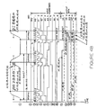
- Figure 4A and 4B show a timing diagram for the address signals generated by the logic for addressing the PROM in the envelope generator 28 to effect generation of the digital values representing the synchronizing signals during the horizontal blanking interval.
- the timing relationships associated with the generation of the digital value representative of the synchronizing signals that occur during the vertical synchronizing interval are similarly generated as will be described in further detail hereinafter with reference to the timing PROM l00 shown on Figure 5B.
- These figures also give the boolean expressions which are true for any particular interval of time marked off by a box defined by the dashed horizontal and vertical lines shown in the figures. Each signal is assigned a time line which is circled and on the left of the signal.
- the signal on line l indicates the timing of the desired sine squared edges where the edges are marked with the same reference letters as they were marked with in Figure 2C.
- This representation on time line l is of course not a real signal, but is, instead, the graphical representation of the times of occurrence and the analog voltage levels of the digital transition edge gain control values if they were converted to a series of discrete analog voltage levels and filtered to smooth out the transitions between these levels.
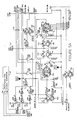
- Figures 5A-5E which together illustrate a diagram of the logic which implements the preferred embodiment of the invention depicted in Figure l.
- the reader is urged to assemble the drawings 5A-5E using the cut lines shown thereon and signal names to match the signals leaving one of the drawings and going to another for ease of understanding.
- the portions of the logic which correspond to the functional blocks of Figure l will be discussed in order so that the particular circuits which comprise each functional block may be identified.
- the manufacturers part number for each integrated circuit in indicated alongside each integrated circuit in abbreviated form which will be apparent to those skilled in the art.
- FIG. 5A and 5B there is shown logic which is shared by the first digital number generator 26 and the second digital number generator 28.
- the input signals COMP BLANKING, COMP SYNC, and BURST GATE are the signals on the lines 30, 32 and 34 from the reference sync signal generator 27.
- the structure of the reference sync signal generator is well known to those skilled in the art, and integrated circuits are commercially available to perform this function.
- the timing of these three signals is indicated in Figure 6 along with the relationships these signals have with the signals at test points TP-2 and TP-3.
- the signals COMP BLANKING, COMP SYNC and BURST GATE generated by the reference sync signal generator 27 indicate the times of occurrence and the duration of all the synchronization signals in the composite video signal for both the horizontal and vertical blanking intervals.
- the edges of these signals are used to signal the start of the process of retrieving the digital transition edge gain control values that define the sine squared edges for the synchronization signals being digitally synthesized.
- Each of the signals from the reference sync signal generator 27 indicates the starting time and the duration of a particular one of the synchronizing signals in the composite video signal. That is, the COMP BLANKING signal on line 30 indicates by its transitions 49 and 47 the starting time and duration of the horizontal blanking interval.
- transitions not shown in Figure 6 indicate the starting time and duration of the vertical blanking interval in the composite video signal.
- the COMP SYNC signal on line 32 indicates the start times and the durations of the horizontal and vertical sync signals, the equalization signals and the serrations in the vertical sync signal.
- the transition 54 and 56 in Figure 6 indicate the beginning and end of the horizontal sync signal during the horizontal blanking interval.
- the BURST GATE signal on line 34 signals the starting times and the durations of the color burst intervals in the horizontal and vertical blanking intervals.
- the transitions 57 and 59 indicate the start and stop of the horizontal blanking interval color burst interval.
- the TP-2 signal also starts the chain of events which cause the proper signals to be generated to control the first digital signal generator to cause it to generate the appropriate digital signal values to represent the particular peak amplitude value needed at any particular time for multiplication by the gain control values.
- the TP-2 waveform marks the time of each transition between the video information and the synchronizing signals and the transitions between the various ones of the sychronizing signals.
- the transition 58 marks the boundary between video information signal and the start of the horizontal blanking interval.
- the transition 60 marks the transition in the horizontal blanking interval of the synchronizing signals from the horizontal blanking level to the horizontal sync level.
- the transition 62 marks the trailing edge of the horizontal sync signal when the voltage level of the final composite video signal is supposed to return to the horizontal blanking level from the peak amplitude level of the horizontal sync signal.
- the transition 64 marks the beginning of the color burst interval while the transition 66 marks the end of the color burst interval.
- the transition 68 marks the end of the horizontal blanking interval.
- a NAND gate 35 having one input coupled to a BURST OFF signal serves to prevent the passage of the BURST GATE signal through to the gate Ull0 under processing conditions when no burst is present, such as processing monochrome signals.
- the reference sync signal generator 27 continues to generate the BURST GATE signal even when monochrome signals are being processed.
- the BURST OFF signal is a command from the user console which is active low, and which causes the gate 35 to block the passage of the BURST GATE signal through to the gate Ull0 thereby preventing the formation of transitions 64 and 66 in the TP-2 signal.
- Each of the existing transitions on the TP-2 signal is converted to one of the pulses on the TP-3 signal illustrated on the time line 5 of Figure 6 by an edge detector circuit comprised of the IC's U95, Ul08, and U72.
- the operation of this edge detector will be apparent to those skilled in the art, and any edge detector design will suffice for purposes of practicing the invention.
- the purpose of the edge detector is to generate a pulse for each transition in the TP-2 signal.
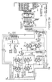
- the IC U72 is a Fairchild 74Fl6l synchronous presettable modulo l6 binary counter which counts the 4Fsc clock pulses (period 70 nanoseconds) when the signal at pin 7 enables the counting.
- the preset inputs of this counter are coupled to the sync to subcarrier phase adjustment circuit l0l ( Figure 5B) and a 25 hertz offset circuit by a bus 70.
- the data on the bus 70 preloads the terminal count into the counter U72.
- the terminal count output, pin l5 goes high, which by the action of the inverter U58 causes the node TP-3 to go low for one clock cycle.
- the pulses on the TP-3 signal at the TP-3 node, shown at time line 5 of Figure 6 can be shifted in time relative to the transitions in the TP-2 signal on time line 4.
- the addressing signals for accessing the edge shaping gain control values from the second digital signal generator are generated starting at the time when TP-3 goes low, as are the signals which control the operation of the first digital signal generator 26.
- the time of the high to low transitions of TP-3 relative to the transitions of TP-2 it is possible to change the times when the addressing signals controlling the second digital signal generator 28 and other signals which control the first digital signal generator 26 occur.
- This is the facility by which the sync to subcarrier phase may be adjusted in coarse fashion one quadrant at a time. It is also the facility by which the generation of the signals which cause the first and second digital signal generators to present the appropriate digital values for multiplication at the appropriate times is coordinated and synchronized with the same clock signal.
- the horizontal sync and horizontal blanking synchronization signals may be shifted relative to the zero crossings in color burst interval, as will be explained in more detail later.
- a course adjustment of the time of occurrence of the sine squared edges of the horizontal sync and horizontal blanking synchronization signals relative to the time of occurrence of the color burst interval can be accomplished. Adjustment is by an integer number of 4Fsc cycles.
- sync to subcarrier phase may be adjusted for any particular television standard with virtually no drift because of the digital and synchronous way in which the adjustment is made.
- the pulses of the TP-3 signal are used to signal when each sine squared transition edge is to be formed. This is illustrated by the time line 2 in Figures 4A and 4B where the TP-3 pulses are shown as negative pulses one of which occurs just before each sine squared transition edge in time line l occurs.
- the signal on TP-3 is used to begin the process of addressing the PROM in the second digital number generator 28 used to store the digital transition edge gain control numbers such that the numbers defining the sine squared transition edges begin to appear on the output of the PROM.
- the proper address signals to access the PROM must be generated.
- the signal on TP-3 in Figure 5A is coupled to the load input of another presettable, modulo l6 binary counter U84 which counts 4Fsc cycles starting from a fixed number hardwired to its preset inputs. This occurs each time a TP-3 pulse loads the preset count.
- the signals A0-A7 on time lines 3-l0 of Figures 4A and 4B represent the binary outputs of the counter U84 and serve as address signals for a timing pulse generation PROM l00 shown in Figure 5B.
- the signal A0 is a divide by two count of the 4Fsc clock pulses on a line 7l.
- the Al signal is a binary division of the A0 signal by 2, and the A2 signal is a binary division of the Al signal by two. Likewise for A3.
- the A4 signal is generated by the flip flops 74 and 76 which are coupled to the terminal count output of the counter U84 and to the 4Fsc clock so that when the count reaches l6, the signal A4 makes a high to low transition on the next 4Fsc clock transition following the terminal count.
- Three more signals, A5, A6 and A7, are generated by the logic shown on Figure 5B to serve as address signals for a timing signal generator in the form of the PROM l00, U85.
- the signal A5 is illustrated on the time line 8 of Figure 4, and is low when the digital transition edge gain control values output by the second digital number generator 28 are supposed to be accessed in a sequence where gain control values in the sequence are increasing from 010 to l.010.
- the signal A5 is high when the digital transition edge gain control values are supposed to be accessed in the reverse order such that the gain control values in the sequence are decreasing from l.010 to 010.
- This is the portion of the logic circuitry referred to earlier which plays a part in controlling whether the sine squared edge being formed is a rising edge or a falling edge. The manner in which this is done will be explained in more detail below.
- the signal A6 on time line 9 in Figure 4 is called the WIDE SYNC signal, and it is in a logic one state starting from a time before the sine squared edge marking the start of the horizontal sync interval is to be formed.
- the A6 signal remains in the logic one state until a time after the sine squared trailing edge of the horizontal sync signal is to be formed.
- the purpose of the WIDE SYNC signal is to provide timing for the first digital signal number generator 26 in the form of a signal SYNC/BURST for which WIDE SYNC is a precursor.
- the SYNC/BURST signal indicates to the first digital signal number generator when the digital signal values defining the peak amplitude of the sync signals are to be presented to the multiplier and when the digital signal value defining the peak amplitude of the burst signal is to be presented to the multiplier.
- the signal A7 illustrated on time line l0 of Figure 4, is called the WIDE BURST signal. It makes a transition to a logic one state starting at a time before the sine squared leading edge of the color burst synchronizing signal "envelope", i.e., the shape defined by the tips of the sine wave cycles of the color burst synchronizing signal, is to be formed.
- envelope i.e., the shape defined by the tips of the sine wave cycles of the color burst synchronizing signal
- the WIDE BURST signal indicates to the second digital signal number generator 28 when the burst interval is occurring, and is used with another signal 625/525 shown on Figure 5D as an address bit for the PROM that stores the gain control values defining the edge shapes for the synchronizing signals in both the horizontal and vertical blanking intervals.
- the WIDE BURST and 625/525 signals define which standard the system is operating under, and cause selection of an appropriate family of gain control values to satisfy the edge shape and rise time requirements of that particular standard. For example, the SECAM standard does not use burst at all, and the PAL standards require a different synchronizing signal rise time than the NTSC standards.
- the particular preload number to the counter U72 and the particular one of the l6 families of gain control bits selected is controlled by input signals from a 25 hertz offset circuit and input signals from a control on the user console which indicates the desired amount of sync to subcarrier phase. These input signals in digital format are added in an adder l0l on Figure 5B, and the 3 most significant bits of the result are coupled by the bus 70 to the preset inputs of the counter U72 of Figure 5A. These three bits select the desired quadrant of coarse sync to subcarrier phase adjustment desired. There are four possible quadrants representing one full subcarrier cycle worth of phase change which may be selected.
- the fine tuning of sync to subcarrier phase is accomplished in response to an SCH phase a dust control signal provided on line 29 through an appropriate operator phase selection device (not shown).
- the 4 least significant bits marked AM3 through AM6 of the result from the adder l0l effects the selection of the particular one of the l6 possible families of edge defining gain control values within the selected quadrant.
- These 4 bits are coupled through exclusive-or gates l03, l04, l05 and l09, and a bus l07 to 4 of the address inputs of the PROM in the second digital signal generator 28, which stores the gain control values to define the edge shapes for the sync and burst synchronizing signals.
- the address bit A5 is coupled as another input to the exclusive-or gates l03, l04, l05 and l09.
- A5 is a logic zero
- the result bits AM3 through AM6 pass through the gates without change.
- A5 is a logic one
- the result bits AM3 through AM6 pass through the gate and are all inverted. This aids selection of the gain control bits defining the appropriate edge direction.
- the PROM l00 responds to the address signals A0-A7 present at its address inputs by issuing timing signals over lines l02 extending to a latch l00a.
- This latch l00a reclocks the timing signals for use by other circuitry of the system, including AM3-AM7 that determine the time periods within which the various sync and blanking intervals occur and AM0-AM2 which signify the time and direction for generation of edge shapes.
- AM3-AM7 that determine the time periods within which the various sync and blanking intervals occur
- AM0-AM2 which signify the time and direction for generation of edge shapes. The manner in which the levels and edge shapes are generated in response to these timing signals will be described in further detail hereinafter.
- the NAND gate 79 has three inputs, a signal on pin l0 related to the TP-3 signal, a signal on pin ll related to the BURST GATE anded with the BURST OFF signal and a REF VERT PULSE signal.
- the REF VERT PULSE signal is low at the leading edge of vertical sync during the vertical blanking interval and stays low for the rest of the vertical blanking interval.
- the purpose of the NAND gate 79 is to affect the generation of the A6 and A7 address signals such that digitally synthesized burst sychronizing signals are not generated when they are not desired, such as when monochrome signals are being processed.
- the timing diagram of Figure 7 shows the signal states of the various signals at the inputs and outputs of the gate 79 under various conditions.
- the signals on time lines l and 2 are the TP-2 and TP-3 signals already discussed. These signals serve as reference points for purposes of study of the rest of Figure 7 to put the signals shown there in context of the overall operation of the system.
- the signal on input pin l0 of gate 79 is shown on time line 3.
- This signal which is the Q not output of flip flop 74, is set to logic one upon the occurrence of each TP-3 pulse, with one exception, because the TP-3 pulses are coupled to the clear input of the flip flop 74.
- the signal on time line 4 of Figure 7 shows the Ull0 input signal on pin l0 during times when there is no BURST GATE signal present. This is the state of the signal for pin l0 of Ull0 when monochrome signals are being processed.
- the input signal on pin ll of gate Ull0 is the inverted BURST GATE signal on the line 34 from the reference sync signal generator 27 after it is buffered and inverted by inverter Ul35 and gated by the BURST OFF signal in the gate Ul09. Suffice it to say that if the BURST GATE signal is shut off, the sine squared "envelope" will have a value corresponding to zero, hence, no transition edges will be generated during the interval when color burst would occur in a color television signal.
- the remaining input to the NAND gate 79 is the REF VERT. PULSE on line 8l.
- This signal acts as described earlier and serves to inhibit the burst related address signals for the PROM l00 during the vertical interval.
- the output signal from the gate Ull0, pin 8 is illustrated on the time line 6 of Figure 7 when the BURST GATE signal is present during color signal processing and on time line 7 of Figure 7 when the BURST GATE signal is not present during monochrome signal processing.
- This signal is coupled to the D input of a reclocking flip flop U95 which is clocked by the 4Fsc reference clock thereby synchronizing the output transitions of the gate Ull0 to the 4Fsc reference clock.
- the Q output of the reclocking flip flop U95, pin 9, is coupled to clock inputs of two D flip flops 83 and 85 of Ul34.
- the operation of Ul34 and a NAND gate 80 in Ull0 is illustrated in the timing diagram of Figure 8.
- the COMP SYNC signal on line 87, illustrated on time line 4 of Figure 8, is coupled to the asynchronous direct set inputs of the flip flops 83 and 85 to set both their Q outputs to logic one on pins 9 and 5 at the time of the high to low transition 54 of COMP SYNC.
- the clock inputs of the flip flops 83 and 85 receive the reclocked output signal from gate Ull0, pin 8.
- transition 286 on the Q output of the flip flop 83 which marks the end of the "wide sync" period. It is irrelevant whether color or monochrome signals are being processed since the sync signal interval is the same in either case.
- the transition 286 on time line 5 occurs after the end of the horizontal sync interval marked by the transition l56 on the COMP SYNC signal, and must be reclocked with the TP-3 signal and the 4Fsc clock signal.
- it is coupled to a flip flop 87 which has its D input coupled to the Q output of a flip flop 89 which has its D input coupled to the TP-3 node and its clock input coupled to the 4Fsc clock.
- the flip flop 87 is clocked by the 4Fsc signal, and generates the signal A6 shown on time line 9 of Figure 4 at its Q output. This signal is a precursor to the WIDE SYNC signal.
- the Q output signal from flip flop 83, time line 5, is also coupled to the D input of the flip flop 85.
- the Q output on pin 5 of the flip flop 85 was set to logic one by the transition l54 of the COMP SYNC signal.
- the Q output of flip flop 85 will be reset to logic zero after the high to low transition 286 in the wide sync precursor signal from the Q output of the flip flop 83 upon the occurrence of a certain condition. That condition occurs at the time of the next low to high transition at the clock input of the flip flop 85.
- the clock input of the flip flop 85 is coupled to the output of the NAND gate 79/flip flop U95, so the next low to high transition will be either the transition 288 or 290 on time lines 2 or 3 depending upon whether the BURST GATE signal is or is not present, i.e., whether color or monochrome signals are being processed.
- the resultant output signal transitions at the Q output of Ul34 are illustrated at 292 and 294 of time lines 6 and 7 in Figure 8 for, respectively, the BURST GATE present and BURST GATE not present conditions.
- This signal at the Q output of the flip flop 85 on line 9l is a precursor signal for the WIDE BURST signal, A7 on time line l0 of Figure 4 in that it defines the duration of the WIDE SYNC signal although not its starting time.
- the starting time of the WIDE BURST signal is established by reclocking the precursor signal with the 4Fsc clock and the TP-3 signal and gating the result with a signal called BRUCH'S BLANKING to be described below.
- the Q output of flip flop 85 on line 9l is gated through a NAND gate 80.
- the NAND gate 80 gates the signal with the BURST OFF signal and the Q not output of the flip flop 83 on line 93 to generate the signal on time line 8 of Figure 8.
- the BURST OFF signal is a logic one when color signals are being processed, so it does not block passage of the signal on the line 9l during color processing, but will block passage of this signal through the gate 80 during times when BURST OFF is a logic zero indicating monochrome processing or other conditions where no digital synthesis of a burst signal is desired.
- Time line 8 does not indicate the condition where BURST OFF prevents the passage of the signal on line 9l through the gate 80.
- the transition 286 on time line 5 will cause the output of the gate 80 to make the transition 295 on time line 8, because the signal on line 9l is a logic one at this time.
- the high to low transition 292 of the signal on line 9l during color processing will cause the low to high transition 252 on time line 8 of Figure 8.
- the time line 8 signal at the output of the gate 97 is another precursor signal for the WIDE BURST signal, A7. All that remains to complete the generation of the WIDE BURST signal is to reclock the signal on line 97 with the TP-3 and 4Fsc signals and to gate it with another signal, BRUCH'S BLANKING.
- the signal on line 97 is reclocked with the 4Fsc signal and the TP-3 signal by flip flops 82 and 84 and gated with the BRUCH'S BLANKING signal in the gate 88 to generate the A7 address signal.
- the address signal A7 is only a precursor of the WIDE BURST signal shown on time line l0 of Figure 4.
- the actual WIDE BURST signal is generated by the PROM l00 by decoding the address signals A0 through A7 to generate the output bit D4 shown on time line l0 of Figure 4.
- the BRUCH'S BLANKING signal is only active during PAL signal processing. In PAL processing during the vertical blanking interval there is one horizontal line interval in each vertical blanking interval which does not have any burst synchronizing signal.
- the time of occurrence of each such horizontal line interval varies in each field of each frame in a cyclical fashion called Bruch's sequence.
- the BRUCH'S BLANKING signal prevents the burst synchronizing signal from being digitally synthesized for these horizontal line intervals in the vertical blanking intervals where no burst is supposed to be present when processing PAL signals.
- Time line 3 illustrates the D input signal at pin l2 of flip flop 82 which is coupled to the output pin l2 of the gate 80.
- This signal is clocked by the 4Fsc clock to cause the Q not output on pin 8 to make the transitions 96 and 98 on the time line 4 which represents the reclocked output of the gate 80.
- the Q not output of the flip flop 84, pin 6, is illustrated on time line 5.
- This signal represents the output of the gate 80 reclocked with the TP-3 signal at pin 3 from the Q output of the flip flop Ul2l.
- the signals on the time lines 4 and 5 are then ANDed by the gate 86 to result in another precursor to the A7 WIDE BURST signal on pin 6 of gate 86.
- the A5 address signal plays a part in controlling the order in which the digital transition edge gain control values are accessed from the PROM in the second digital number generator 28.
- the PROM l00 decodes the address signals A0 through A7 and generates output bits D0 through D7 according to a truth table which can be derived from Figure 4.
- the output bits D3 through D7 are the signals on the output lines marked D3 through D7 from the latch U97.
- the D0 through D2 output bits are the envelope shaping address bits AM0 through AM2 on the bus l20 coupled to the address port of a pair of PROMs U99 and lll on Figure 5D.
- the state of these address bits AM0 through AM2 is indicated as the state of the three bits D0 through D2 on time line lA of Figure 4.
- time line l the three bits D0 through D2 decode the address bits A0 through A7 in the sequence 7, 6, 5, ...0.
- the address bits A0 through A7 define 8 addresses during the 8 clock cycles of the edge formation which are different from the 8 addresses defined by A0-A7 during the formation of edge A.
- the contents of the eight addresses accessed during the formation of the edge B define 8 bit patterns for the bits D0 through D2 which are the addresses provided to the pair of PROMs U99 and lll for the 8 sample points for the sine squared edge gain control values of a sine squared edge accessed in the sequence 0, l, 2, ...7.
- the sequences for all the other edges are as indicated on time line lA in Figure 4.
- the A5 signal aids in the process of changing the order of access of the gain control values by inverting the bits which select the particular one of the l6 families of curves selected by the address bits AM3 through AM6 provided on the address bus l20 by the adder l0l ( Figure 5B).
- Figure 5B The reason for this can be seen from inspection of Figures 2 and 3. If the address bits AM3-AM6 select the edge E1, inverting the AM3-AM6 bits results in the selection of the edge E16. The reason this is necessary is best explained by an example.
- the 8th value becomes the first gain control value by which the digital signal value representing the peak amplitude -ll4 is multiplied and the 7th gain control value becomes the 2nd gain control value used in the multiplication.
- the 8th and 7th gain control values for the edge E1 would have to be the different values as the lst and 2nd gain control values for E1 are. This is not true for E1.
- the edge E16 so the A5 address bit inverts the address bits AM3-AM6 to cause the edge E16 to be selected for retrieval of its gain control values during formation of the edge 50.
- the A5 signal is generated by the flip flop 90 which reclocks the TP-2 signal at its D input with the TP-3 signal, as reclocked by the flip flop 89 with the 4Fsc clock signal.
- the signals A0-A7 are used as address inputs to the timing PROM l00 which generates the signals shown on the time lines ll-l5 of Figure 4. These signals provide timing for the digital synthesis of the horizontal blanking, horizontal sync, vertical blanking, the serrations in the vertical sync interval, and the equalizer pulse sychronizing signals.
- the purpose of the PROM l00 is to decode the address signals A0 through A7 to generate the signals shown on the time lines ll-l5 in Figure 4. This simplifies the generation of the above noted timing signals.
- the PROMS U99 and Ulll cannot be addressed directly using the A0 through A7 address signals because there is a need which will be described below for generation of the timing signals shown on the time lines ll-l5 of Figure 4.
- the Boolean expressions pointing to various times on the time lines in Figure 4 indicate addresses which will cause the output on the bus l02 of a particular binary word.
- Each bit of each of these binary output words has the logical state indicated for the signal ocorresponding to that bit on the time lines ll-l5 in Figure 4.
- the corresponding condition of the address bits A0-A7 that cause the generation of each output binary word D0-D7 at any particular time are reflected in the Boolean expression of the address bits corresponding to that particular time.
- These binary output words are reclocked by a latch l04 comprised of 8 D type flip flops clocked by the 4Fsc clock at pin ll.
- the outputs of these latches are the signals: SYNC/BURST, NARROW BLKG B, WIDE BLANKING, WIDE BURST, NARROW BLKG A, and ENVELOPE SHAPING AM0 through AM2.
- SYNC/BURST NARROW BLKG B
- WIDE BLANKING WIDE BURST
- NARROW BLKG A ENVELOPE SHAPING AM0 through AM2.
- the SYNC/BURST signal on time line l4 is low from the leading edge of the horizontal blanking interval to the end of the horizontal sync interval whereupon it goes high during the burst period and stays high until the next start of blanking. This signal makes a similar transition during the vertical blanking interval.
- the SYNC/BURST signal is coupled to an input of the first digital signal number generator 26 to signal that logic when the transition between sync and burst occurs. This causes the first digital signal number generator to change the digital signal value at its output from the value representing the peak amplitude of sync to the values representing the peak amplitudes of the burst signal.
- Figure 5C shows that the multiplexer 22 has the input for receiving the output of the first digital signal number generator coupled by a bus l08 to the outputs of two multiplexers U6l and U6l. These multiplexers output l0 bit digital data representing the magnitude and sign of the peak amplitudes of all synchronizing signals.
- Figure l0B represents the binary bit patterns which represent the peak amplitudes of the synchronizing signals to be generated and their relationship to the signals depicted in Figure l0A.
- the signals in Figure l0A represent the signals which generate and are the bit patterns shown in Figure l0A.
- the identification of which lines represent which bits is indicated by the bit significance indicators such as 20 written above each line from the output of the multiplexers U6l and U62.
- the line labelled 20 is the least significant bit in the l0 bit data and is coupled to pin ll of U76.
- the NTSC standard requires that the equalizing pulses and the serrations in the vertical sync interval start from the same level as the horizontal sync pulse and have the same peak amplitude as the horizontal blanking level. It is also well known that the vertical sync interval starts from the horizontal blanking level and has a peak amplitude equal to the peak amplitude of the horizontal blanking level.
- the remaining synchronizing signals in the interval of the vertical blanking interval following the post equalizing pulse interval are repetitions of the synchronizing signals in the horizontal blanking interval.
- the color burst interval is present in the vertical blanking interval portion following the post equalizing interval only if color video information signals are being processed. Different digital peak amplitude levels are used for PAL standard synchronizing signal generation.
- the bit patterns for the sync, blanking and burst synchronizing signals show certain characteristic patterns which are used to advantage in simplifying the circuit of the first digital signal number generator 26. For example, all the bits in the bit positions 27, 28 and 29 (the sign bit) are always the same and only toggle between the logic zero and the logic one state to represent certain levels. As a consequence, the lines representing these bits are ganged together. The same is true for the bits in the bit positions 24 and 25. All the other bits are unique.
- the SYNC/BURST signal is a logic one and the WIDE BURST is a logic one.
- These two signals are coupled to the preset and clear inputs of two flips l87 and l89 as shown in Figure 5C. Both of these flip flops are Fairchild Fast 74F74's.
- both of the flip flops l87 and l89 will be free running in sychronization with the 4Fsc clock signal and without interference from signals at their preset and clear inputs, both of which are active low.
- the result is as follows during the burst intervals.
- Both flip flops are clocked by the 4Fsc clock pulses.
- the D input of the flip flop l87 is coupled to a clock running at an Fsc rate through the inverter U74 and the exclusive-or gate U70.
- the other input of the exclusive-or gate U70 is coupled to a decoder (not shown) which decodes signals from the user console indicating which television standard is to guide processing.
- This signal either inverts the Fsc clock signal through the exclusive-or gate or passes it through the gate without inversion depending upon the standard in effect.
- the D input of the flip flop l89 is coupled to the 2Fsc clock through an exclusive-or gate l9l, which either inverts the 2Fsc clock signal or passes it uninverted depending upon the state of the NTSC(-) standards determining signal decoded from inputs from the user console.
- this signal is a logic zero, and the gate l9l is transparent.
- the Q output of the flip flop l89 will thus toggle from logic zero for 2 cycles of the 4Fsc clock to logic one for 2 cycles of the 4Fsc clock.
- This output is coupled through an inverter U63 to the enable inputs of the two multiplexers U6l and U62 by the line l93.
- the multiplexer outputs When the signal on the line l93 is a logic zero, the multiplexer outputs will be enabled and will present the bit pattern of the selected input on the output bus l08. When the multiplexer outputs are not enable, they will present an all zero bit pattern on the output bus l08. These all zero bit patterns represent the zero base-line level of the burst signal shown in Figure 2B. The zero level base-line segments will ultimately represent the burst zero crossings in the analog filtered output.
- the particular input of the multiplexers U6l and U62 which is selected is controlled by a signal 625/525 from the standards decoder (not shown). This signal indicates which of the various standards is in effect. Since the peak amplitude levels for the various synchronization signals are different under the different standards, the input data for the A and B inputs to the multiplexers U6l and U62 are set so that one input data pattern represents the peak amplitude levels for sync and burst under one standard and the other input data pattern represents the peak amplitude levels for the sync and burst signals under another standard. The signal 625/525 then selects the appropriate input data pattern depending upon the particular standard then in effect.
- the peak amplitudes alternate sequentially from 0 to +57, then back to 0, then to -57, then back to 0 to complete one complete cycle of subcarrier, i.e., one Fsc clock cycle.
- the signal on line l93 controls the transitions of the output bits to the 0 level by disabling the outputs of the multiplexers U6l and U62 at the appropriate times, as will be appreciated by those skilled in the art.
- the exclusive-or gates l95 and l97 combine with the flip flops l87 and l89 and the inverter U63 to decode the input signals described above to cause the appropriate bit patterns to appear on the A and B inputs of the multiplexers U6l and U62 at the appropriate times and for the appropriate durations.
- the manner in which this decoding is done will be apparent to those skilled in the art from a study of the interconnections shown in Figure 5C, the timing of the signals shown on Figures 4 and l0 and from the various bit patterns under the NTSC standard shown on Figure l0B.
- This decoding at the inputs of the multiplexers causes the appropriate digital signal values representing the peak amplitudes of the various synchronizing signals in the horizontal and vertical blanking intervals to appear at the appropriate times and the appropriate durations for the various standards on the output bus l08, which is coupled through the multiplexer 22 at appropriate times to the A input of the multiplier 20.
- the WIDE BURST signal is a signal which indicates the presence of a burst interval. It will not be generated when the BURST GATE and BURST OFF(-) signals indicate no burst is to be generated. WIDE BURST goes high before the start of the color burst interval during color processing under certain standards, i.e., the edge D on time line l in Figure 4, and goes low after the end of the burst interval, i.e., the edge E on time line l.
- the WIDE BURST signal is used to preset the flip flop l87 Q and Q not outputs to a logic one during the sync intervals, and is used as one address bit to the PROMs U99 and lll along with the 625/525 standard defining signal to prevent a burst from being formed under certain standard dependent conditions.
- WIDE BLANKING signal and NARROW BLANKING A and NARROW BLANKING B signals will be discussed below in conjunction with the logic to which they are coupled.
- the only difference between the NARROW BLANKING A and NARROW BLANKING B signals is that one is slightly delayed from the other and can be used for timing logic downstream where propagation gate delays have delayed the arrival of signals to be timed thereby.
- the multiplier 20 is a TRW ll2KJ4C which accepts one digital number at its A inputs Y0-Yll and multiplies it by another digital number it receives at its B inputs X0-Xll.
- the A inputs are coupled to the outputs of two AMD2982l high performance bus interface registers U77 and U76 which form the multiplexer 22.
- Each of these flip flops consists of a plurality of D flip flops having their D inputs coupled to the input port consisting of pins 2-ll and having their clock inputs ganged to a pin l3 which is coupled to the 4Fsc clock signal.
- Each of these flips flops has its Q output coupled to one of the output pins l4 through 23 all of which are simultaneously enabled or disabled by the state of an output enable signal at a pin l which is coupled to a gating circuit to be described in more detail below.
- the flip flop U77 has its inputs coupled to the level shifted, l0 bit, 2's complement format digital video data on a bus l06 from the video signal processor 24.
- U76 has its inputs coupled to a bus l08 which carries the digital signal values which define the peak amplitudes of the various synchronizing signals.
- the multiplexer 22 couples either the outputs of U77 or of U76 to the A inputs, i.e., the A input on Figure l, depending upon which one of them is enabled by the gating circuit.
- the gating circuit is coupled to the NARROW BLANKING A signal from the timing PROM l00, and enables the U76 latch outputs during the horizontal and vertical blanking intervals. This connects the digital signal values from the first digital signal number generator 26 to the A input of the multiplier when the peak amplitude digital signal values are to be inserted into the stream of video information digital data coming in on the bus l06. This allows the formation of new digital format synchronization signals.
- the switching action by the multiplexer 22 is controlled by the horizontal blanking signal NARROW BLANKING A which is gated with a signal SECAM BOTTLE EN (-) by the gates ll4, ll6 and ll8.
- SECAM BOTTLE EN (-) signal is a logic one during all NTSC and PAL operation and only is asserted at the logic zero level during the vertical blanking interval of SECAM operation. Thus for all of the time during NTSC and PAL operation, SECAM BOTTLE EN (-) is a logic one.
- the NARROW BLANKING A signal is a logic one during the time from just after the leading edge of blanking, i.e., edge A in Figure 4, to a time just before the trailing edge of blanking, i.e.,the edge F in Figure 4.
- NARROW BLANKING A is a logic one
- SECAM BOTTLE EN (-) is a logic one
- the gate ll6 output is low thereby enabling the sync and burst latch U76 and passing the digital data from the first digital signal number generator 26 through to the A input port of the multiplier 20.
- the gate ll4 inverts NARROW BLANKING A signal thereby causing the gate ll8 to disable the multiplexer latch U77 outputs.
- NARROW BLANKING signal is used to generate the enabling signals to U77 and U76 of the multiplexer 22 is because the video is at blanking level and the multiplier gain is zero at the edge transitions of the narrow blanking signal. This prevents generation of spurious signals during the switching action of the multiplexer.
- a new overlapping blanking signal could be coupled to the A inputs of the multiplier 20 to be multiplied by the gain numbers on the bus 42 instead of relying on the blanking pulse in the original video. Reliance on the original signal blanking pulse is used in the preferred embodiment, because the timing of the blanking is not as critical as that of sync and burst, and it makes the circuit simpler.
- the digital signal values from the first digital number generator 26 are multiplied in the multiplier 20 by the digital transition edge gain control numbers ranging in the decimal number system from 0 to l.0. These gain control numbers are retrieved from the PROMs U99 and lll in Figure 5D, and applied to the B input of the multiplier 20 by a bus 42.
- the PROM U99 stores gain control numbers to define the edge shapes for only the horizontal and vertical synchronizing signals, the pre and post equalizing pulses and the serrations in the vertical sync pulse.
- the digital transition edge gain control values which define the edge shapes for the horizontal and vertical blanking intervals are stored in the PROM Ulll for reasons which will be made clear below.
- the gain numbers on the bus 42 are digital numbers which would represent the transition edge gain control numbers.
- they would, if converted to analog voltages, represent the waveform on time line l of Figure 4A.
- the digital transition edge gain control numbers would in analog voltage form define a signal similar in nature to that on time line l of Figure 4 except that it would define the times of occurrence and shape of the edges of the synchronization signals in the vertical blanking interval, viz., the pre and post equalizing pulses, the vertical sync interval and the serrations therein, and the horizontal blanking interval signals following the post equalizing pulse interval in the vertical blanking interval.
- the multiplier 20 B inputs receive digital gain control numbers sent from a user console on a bus 42 through a decoder U45, a reclocking latch U60, the bus ll0′ and the latch ll3 for the purpose described above.
- the advantage of this is that a digital gain control function for the video information signals can be simply implemented without adding very much new circuitry. This also makes more effective use of the multiplier 20 which is quite expensive. By using it during times when it would otherwise be idle if used solely for digital synthesis of the synchronizing signals, the whole system is rendered more cost effective.
- the digital transition edge gain numbers which define the desired edge shape for the horizontal and vertical blanking synchronization signals is stored in PROM Ulll.
- This PROM store gain control numbers for a 525 line NTSC standard video blanking pulse.
- Another PROM (not shown) is used to store the gain numbers defining the desired edge shape for the horizontal and vertical blanking synchronization signals used in the 625 line PAL standard.
- the PROM Ulll is enabled only during the intervals during which the leading edge and trailing edges of the vertical and horizontal blanking intervals are being formed. The reason that the gain control numbers for the blanking synchronizing signals are not stored in the PROM U99 is that the rise times of the blanking intervals vary arbitrarily with the gain setting.
- edges of the blanking synchronization signals must make a smooth, precisely shaped transition from the amplitude level of the video information signal to the blanking level. Since the video information signal level is dependent upon the gain level set by the operator, special circuitry is needed to accomodate the varying video information gain level.
- This special circuitry is the PROM Ulll and a bus 20l which couples video information gain control data into the address inputs of the PROM.
- the PROM Ulll has stored therein several families of gain control values. Each family defines a sine squared shape which make a transition from a particular video amplitude level to the blanking level.
- the address inputs coupled to the bus 20l receive a bit pattern which is set by the operator and which defines the desired video gain level.
- the bus 20l is coupled to the 5 most significant bits of the output of the latch U45. This latch receives video gain control data from the operator console.
- the bits on the bus 20l cause the selection of the proper family of gain control values for the video gain level existing at the start of any particular blanking interval whether it is horizontal or vertical blanking.
- the PROM Ulll is enabled only during the intervals when the leading and trailing edges of the blanking intervals are being formed by ANDing the NARROW BLANKING and the WIDE BLANKING signals together. From Figure 4, time lines l2 and l3 it is seen that if these two signals are ANDed, the result will be a pulse which has a duration equal to the difference in times between the transition 203 on time line l2 and the transition 206 on the time line l3. This is the interval during which the edge A on time line l is being formed which is the leading edge of the blanking interval. A similar result occurs for the edge F which is the trailing edge of the blanking interval where the pulse has the duration equal to the time between the transition 207 and 209.
- This AND function is implemented by the NAND gate 2ll on Figure 5D.
- This gate has as its two inputs the properly inverted WIDE BLANKING and NARROW BLANKING A signals.
- the output of the gate 2ll is coupled to the chip select input of the PROM Ulll which is active low. This results in the PROM Ulll being active only during the proper intervals.
- the particular one of the families of gain control values is selected, the particular one of the gain control values which is output at any particular time is established by the bit pattern on the bus l20 which carries the address bits AM0 through AM2 from the timing PROM l00. The order of retrieval of these gain control values is controlled as is done for the PROM U99.
- the address bits AM0 through AM2 are generated from the A0 through A7 address bits generated by the logic on Figures 5A and 5B.
- the logic on Figures 5A and 5B generates the A0 through A7 address bits and the timing signals based upon the incoming reference sync and clock signals from the reference sync signal generator which is itself running synchronously with the house reference clock signal. Since the video information processing signal is also running synchronously with the house reference clock, it is seen that the timing of the edge formation of the various synchronizing signals can be precisely controlled relative to the video information signal.
- the PROM addressing bits on the bus l20 cycle through the addresses to select the transition edge gain control number l-8 sequentially.
- the transition edge gain control numbers output from the PROM are placed on a bus 42 and reclocked through a latch ll3 clocked by the 4Fsc clock.
- the gain control values are then coupled to the B input port of the multiplier 20 and are used to multiply the numbers at the A input thereby producing the output stream of digital numbers at port C of the multiplier.
- Figure 5E shows the logic of the video signal processor 24.
- the video signal processor 24 subtracts l2810 digital levels from the incoming digital video information samples entering from the left on the bus 38 by adding 384 digital levels to the incoming binary data.
- These video information samples of the incoming binary data are digital numbers representing the results of an analog to digital conversion of the video signal at a certain sampling rate. In the preferred embodiment, the sample rate is 4 times the subcarrier frequency.
- the video signal processor also converts the digital video sample data to two's complement form to make it compatible with the operation of the multiplier 20.
- the video signal processor converts the incoming 9 bit data to l0 bit data by adding a sign bit which is 0 for levels above the blanking level and l for levels below the blanking level.
- the overall effect of the video signal processor is to convert the blanking level, which is at l2810 in the incoming video data to 010 in the outgoing 9 bit 2's complement data and to add a sign bit as the l0th bit.
- the above described function is done with three 4 bit binary full adders with carry ll5, ll7 and ll9, a clocking latch l23 and a reclocking latch l25.
- the incoming digital data is coupled into the B inputs of the adders through the clocking latch l23, which is clocked by the 4Fsc clock so that its arrival at the adders is synchronous with the rest of the system.
- the carry out of each adder is coupled to the carry in of the adder for the nibble of next higher significance.
- the carry out of the most significant adder ll9 is coupled through an inverter l2l to the l0th bit of the output data bus l06′.
- the B inputs of these adders are coupled to the 9 bit digital video information input data.
- the B3 input of the adder ll5 is the least significant bit of the input data, CL0, and the B3 input of the adder is the most significant bit of the 9 bit input data, CL8.
- This binary video information input data has levels which vary from 010 to 5l210 with sync tip at l4 and blanking level at l28.
- the object is to convert the blanking level to 010 and to add a sign bit as the l0th bit thereby converting to two's complement format.
- 38410 is added to the input binary and the overflow out the carry of the adder ll9 is inverted and coupled to the l0th bit or sign bit of the output bus l06′. This is done as follows.
- the A inputs of the adders are coupled by a bus 37 to an 8 bit number comprised of the bits B0 through B7 from a constants generator.
- the constants generator is actually a black level adder, but for purposes of the invention, the bits B0 through B7 carry a bit pattern equal to l2810. That is, bit B7 is a logic one, and all other bits are logic zeroes.
- the B2 and A2 inputs of the adder ll5 are grounded to keep them from floating. Thus if the bus 37 were alone, only l28 would be added.
- the A3 input of the adder ll9 is also coupled to a logic one by the wire 43 which represents a binary number l 0000 0000 or 2 ⁇ l09 which equals 256.
- the output of the multiplier 20 on the bus 5l is a stream of digital numbers representing the composite video signal with digitally controlled video gain and new, digitally synthesized horizontal sync, equalizing pulses, vertical sync interval, serrations in the vertical sync interval, color burst and horizontal and vertical blanking synchronizing signals.
- the circuitry that may be used to implement the digital to analog conversion of the converter 39 and the filtering of the filter 41 in Figure 1 is well known to those skilled in the art, and will not be described here.
Landscapes
- Engineering & Computer Science (AREA)
- Multimedia (AREA)
- Signal Processing (AREA)
- Processing Of Color Television Signals (AREA)
Claims (52)
- Appareil servant à générer numériquement un signal de synchronisation, comprenant: un premier moyen (26) servant à fournir au moins une valeur de signal numérique qui représente une crête d'amplitude dudit signal de synchronisation; un second moyen (28) servant à fournir au moins un ensemble de valeurs de commande de gain numériques qui constituent une représentation numérique de la forme de bord dudit signal de synchronisation, lesdites valeurs de commande de gain apparaissant en synchronisation avec le début et la fin de chaque intervalle de signal de synchronisation; un moyen (20) servant à multiplier chacune des valeurs de commande de gain numériques d'un ensemble provenant dudit second moyen par une valeur de signal numérique correspondante en provenance dudit premier moyen et à délivrer des signaux numériques représentant les produits numériques desdites multiplications; et un moyen de génération de signal de référence (27) servant à fournir des signaux de rythme de référence communs définissant les intervalles de signaux de synchronisation et des moyens (30, 32, 34) servant à relier les signaux de rythme de référence au premier moyen (26) ainsi qu'au second moyen (28) afin de commander le rythme de la délivrance de la valeur ou des valeurs de signaux numériques et de l'ensemble des valeurs de commande de gain respectivement.
- Appareil selon la revendication 1, comprenant en outre un moyen (39) pour convertir lesdits produits numériques en un signal de synchronisation analogique.
- Appareil selon la revendication 1, comprenant en outre un moyen (24) pour fournir un signal vidéo et un moyen (22) pour insérer ledit signal de synchronisation dans un intervalle prédéterminé dans ledit signal vidéo.
- Appareil selon la revendication 1, dans lequel ledit second moyen (28) enregistre au moins un ensemble de valeurs de commande de gain numériques qui constituent une représentation numérique d'une forme de bord en sinus carré.
- Appareil selon la revendication 1 ou la revendication 4, dans lequel ledit second moyen (28) enregistre un seul ensemble de valeurs de commande de gain numériques qui définissent tous les bords dudit signal de synchronisation.
- Appareil selon la revendication 1 ou la revendication 4, dans lequel ledit signal de synchronisation comprend un signal de synchro et un signal de salve se composant d'une multiplicité de cycles d'un signal de sous-porteuse et dans lequel ledit second moyen (28) enregistre une famille d'ensembles de valeurs de commande de gain numériques dans laquelle chaque ensemble définit les formes de tous les bords dudit signal de synchronisation et chaque ensemble présente un rapport de phase synchro à sous-porteuse différent.
- Appareil selon la revendication 6, dans lequel le second moyen (28) est agencé pour recevoir lesdits signaux de rythme de référence et pour générer à partir de ceux-ci des signaux d'adresse afin d'accéder à un ensemble spécifique de ladite famille d'ensembles de valeurs de commande de gain et d'accéder aux valeurs de commande de gain de l'ensemble sélectionné pour les relier audit moyen de multiplication.
- Appareil selon la revendication 7, comprenant en outre un moyen (29) permettant à l'utilisateur d'introduire un signal indiquant le rapport de phase synchro à sous-porteuse voulu et réagissant audit signal en faisant générer lesdits signaux d'adresse pour sélectionner l'ensemble approprié de valeurs de commande de gain présentant le rapport de phase synchro à sous-porteuse sélectionné.
- Appareil selon la revendication 7, comprenant en outre un moyen de multiplexage (22) comportant une entrée d'informations vidéo et une entrée servant à recevoir des valeurs de signaux numériques en provenance dudit premier moyen (26) et comportant une entrée de commande reliée en vue de recevoir un signal de rythme de référence commandant la commutation entre lesdites entrées et dans lequel ledit moyen (20) de multiplication comporte une première entrée reliée à la sortie dudit moyen de multiplexage et une seconde entrée reliée à la sortie dudit second moyen.
- Appareil selon la revendication 9, comprenant en outre un moyen de commande de gain numérique servant à recevoir un signal d'entrée en provenance d'un utilisateur et à fournir des valeurs de commande de gain d'information vidéo numériques audit moyen de multiplication pour commander le gain dudit signal d'information vidéo.
- Appareil selon la revendication 10, dans lequel ledit signal de synchronisation comprend un signal de suppression et dans lequel ledit second moyen (28) comprend un moyen de mise en forme de bord de suppression servant à enregistrer une multiplicité d'ensembles de valeurs de commande de gain de bord de transition de suppression numériques qui définissent les formes d'une multiplicité de bords pour ledit signal de suppression, chacun desdits ensembles de valeurs de commande de gain numériques de bord de transition de suppression définissant la forme d'un bord de suppression depuis un niveau de gain particulier jusqu'au niveau de suppression, ledit moyen de mise en forme de bord de suppression comportant des entrées d'adresse reliées audit moyen de commande de gain numérique en vue de recevoir des signaux indiquant le niveau de gain courant, lesdits signaux d'adresse entraînant la sélection de l'ensemble approprié de valeurs de commande de gain de bord de transition de suppression relativement au niveau de gain courant.
- Appareil selon la revendication 11, dans lequel ledit moyen de mise en forme de bord de suppression comprend des entrées d'adresse reliées en vue de recevoir des signaux d'adresse qui entraînent l'accès des valeurs de commande de gain de bord de transition de suppression en provenance de l'ensemble sélectionné en vue de les relier à ladite seconde entrée dudit moyen de multiplication.
- Appareil selon la revendication 5, dans lequel ledit second moyen (28) est une mémoire comportant des entrées d'adresse, des entrées de commande et des sorties de données et comprenant en outre un moyen pour générer une multiplicité de signaux d'adresse et de commande qui sont reliés auxdites entrées d'adresse et de commande pour faire en sorte que ladite mémoire délivre de façon synchrone lesdites valeurs de commande de gain à des moments appropriés pour définir les bords dudit signal de synchronisation de façon à ce qu'ils aient une forme en sinus carré.
- Appareil selon la revendication 5, comprenant en outre un moyen pour inverser la séquence d'accès desdites valeurs de commande de gain pendant la formation de bords prédéterminés.
- Appareil selon la revendication 5, dans lequel ledit second moyen (28) est une mémoire comportant des entrées d'adresse, des entrées de commande et des sorties de données et ledit moyen complémenteur comprend un moyen pour générer une multiplicité de signaux d'adresse et de commande qui sont reliés auxdites entrées d'adresse et de commande de façon à faire en sorte que ladite mémoire délivre de façon synchrone lesdites valeurs de commande de gain suivant une première séquence au moment approprié pour définir un premier bord dudit signal de synchronisation et de façon à faire en sorte que ladite mémoire délivre de façon synchrone lesdites valeurs de commande de gain suivant une séquence inverse au moment approprié pour définir un second bord dudit signal de synchronisation.
- Appareil selon la revendication 3, dans lequel ledit moyen d'insertion (22) est un moyen de multiplexage ayant une sortie et une entrée de commande reliée à un signal de rythme de référence, ledit moyen de multiplexage étant conçu pour sélectionner soit ledit signal vidéo, soit ledit signal de synchronisation, en vue de le relier à ladite sortie en fonction de l'état dudit signal de rythme de référence.
- Appareil selon la revendication 16, dans lequel ledit moyen de multiplexage (22) comprend un multiplexeur ayant une première entrée reliée audit moyen (24) servant à fournir un signal vidéo et une seconde entrée reliée audit premier moyen (26), ledit moyen de multiplication (20) comprenant un multiplicateur numérique ayant une première entrée reliée à ladite sortie dudit multiplexeur et une seconde entrée reliée audit second moyen (28).
- Appareil selon la revendication 17, comprenant en outre un moyen (39) relié audit moyen de multiplication (20) servant à convertir lesdits produits numériques en un signal de synchronisation analogique.
- Appareil selon la revendication 3, dans lequel ledit moyen (24) servant à fournir un signal vidéo fournit des valeurs numériques représentant l'amplitude d'un signal vidéo, lesdites valeurs numériques étant fournies en synchronisme avec un signal d'horloge.
- Appareil selon la revendication 19, dans lequel ledit premier moyen, ledit second moyen et ledit moyen de multiplication sont tous reliés au même signal d'horloge (36) qui commande le rythme de la sortie desdites valeurs vidéo numériques en provenance dudit moyen de fourniture dudit signal vidéo.
- Appareil selon la revendication 3, dans lequel ledit moyen (22) d'insertion est un moyen de multiplexage ayant une première entrée reliée audit moyen de fourniture d'un signal vidéo et ayant une seconde entrée reliée audit premier moyen, et ayant une entrée de commande reliée audit moyen de fourniture d'un signal de référence et ayant une sortie, ledit moyen de multiplexage étant disposé de façon à relier soit ladite première entrée soit ladite seconde entrée à ladite sortie en fonction de l'état dudit signal de référence, ledit moyen de multiplication (20) comprenant en outre un multiplicateur numérique ayant une première entrée reliée à ladite sortie dudit multiplexeur et ayant une seconde entrée reliée audit second moyen.
- Appareil selon la revendication 21, comprenant en outre des moyens (39, 41) servant à convertir lesdits produits numériques en provenance dudit multiplicateur en un signal de synchronisation analogique.
- Appareil selon la revendication 22, dans lequel lesdits moyens (39, 41) de conversion comprennent un convertisseur numérique analogique (39) dont l'entrée est reliée audit multiplicateur et qui comporte une sortie, et un filtre passe-bas (41) dont l'entrée est reliée à la sortie dudit convertisseur numérique analogique.
- Appareil selon la revendication 22, dans lequel ledit filtre (41) présente une fréquence de coupure supérieure approximativement égale à deux fois la fréquence de la sous-porteuse couleur de télévision et une bande de blocage supérieure qui diminue jusqu'à au moins moins six décibels à une fréquence égale à deux fois la fréquence de la sous-porteuse couleur et jusqu'à au moins moins cinquante-cinq décibels à une fréquence égale à trois fois la fréquence de la sous-porteuse couleur.
- Appareil selon la revendication 3, comprenant en outre un moyen pour convertir le signal vidéo en une représentation numérique de complément à deux où le niveau zéro est au niveau de suppression d'un signal de synchronisation de télévision.
- Appareil selon la revendication 25, dans lequel lesdites représentations numériques de complément à deux ont un signe positif prévu pour les valeurs de luminance croissante et ont un signe négatif pour toutes les valeurs plus négatives que le niveau de suppression.
- Appareil pour la génération numérique d'un signal de synchronisation ayant des bords de forme prédéterminée en vue de son insertion dans un signal vidéo afin de former un signal vidéo composite, comprenant: un moyen pour générer séquentiellement une multiplicité d'adresses; un moyen formant mémoire (28) pour enregistrer une valeur de commande de gain numérique à chacune desdites adresses, lesdites valeurs de commande de gain numériques ayant des grandeurs qui définissent la forme desdits bords, et pour délivrer en sortie la valeur numérique enregistrée à chacune desdites adresses lorsque ladite adresse est générée; un moyen (20) pour multiplier chacune desdites valeurs de commande de gain numériques par une valeur de signal numérique qui représente un signal pré-établi qui présente une amplitude prédéterminée au moins pendant les moments de délivrance desdites valeurs de commande de gain numériques de façon à délivrer en sortie le signal de synchronisation voulu; et un générateur de signal de rythme de référence (27) conçu pour fournir des signaux de rythme communs définissant un intervalle de temps de signal de synchronisation et qui commandent le déclenchement de la génération desdites adresses et la fourniture du signal pré-établi.
- Appareil selon la revendication 27, dans lequel ledit moyen de génération séquentielle d'adresses génère lesdites adresses en synchronisme avec un signal d'horloge de référence d'un système vidéo numérique.
- Appareil selon la revendication 28, dans lequel ladite horloge de référence est le signal d'horloge d'échantillonnage d'un correcteur de base de temps numérique.
- Appareil selon la revendication 27, dans lequel ledit moyen formant mémoire enregistre des valeurs de commande de gain numériques définissant la forme des bords des impulsions de suppression et de synchronisation d'un système vidéo.
- Appareil selon la revendication 30, dans lequel ledit moyen formant mémoire enregistre également des valeurs de commande de gain numériques définissant la forme de l'enveloppe de salve d'un système vidéo.
- Appareil selon l'une quelconque des revendications 27 à 31, dans lequel ledit moyen formant mémoire est une mémoire non volatile.
- Appareil selon l'une quelconque des revendications 27 à 32, comprenant en outre un moyen servant à commuter une première entrée dudit moyen de multiplication sur une source de données vidéo numérisées et une seconde entrée sur un point d'accès pour la réception d'un nombre de commande de gain.
- Appareil selon la revendication 33, comprenant en outre un moyen servant à convertir lesdites données vidéo numérisées en un nombre de complément à deux ayant une valeur de zéro au niveau de suppression et des valeurs positives pour des niveaux vidéo de plus grande luminance et des valeurs négatives pour des niveaux plus négatifs qu'un niveau de suppression de signal de synchronisation de télévision.
- Appareil selon l'une quelconque des revendications 27 à 34, dans lequel lesdites valeurs de commande de gain numériques définissent une forme de bord en sinus carré.
- Appareil selon l'une quelconque des revendications 27 à 35, comprenant en outre un moyen de génération de signal servant à générer ledit signal pré-établi sous la forme d'un signal numérique qui représente une amplitude fixe prédéterminée commençant à un moment avant le moment auquel le signal de synchronisation est censé se produire dans le signal vidéo et finissant après la fin de chacun desdits signaux de synchronisation.
- Appareil selon la revendication 36, comprenant en outre un moyen servant à générer une représentation numérique des amplitudes de crête d'un signal de synchonisation de salve commençant à un moment avant le moment auquel le signal de synchronisation de salve est censé se produire dans le signal vidéo composite et finissant à un moment après celui auquel le signal de synchronisation de salve est censé finir dans le signal vidéo.
- Appareil selon la revendication 36, dans lequel le moyen (20) de multiplication reçoit le signal pré-établi en provenance dudit moyen de génération de signal à un moment sensiblement égal au moment auquel le bord avant d'une impulsion de suppression horizontale apparaît dans le signal vidéo entrant.
- Procédé de formation d'un bord d'un signal de synchronisation vidéo, comprenant les étapes consistant: à générer un signal numérique représentant une amplitude de crête prédéterminée dudit signal de synchronisation dans un intervalle commençant avant le moment où ledit bord doit commencer et finissant après le moment où ledit bord doit finir; à multiplier ledit signal numérique par chacune d'une multiplicité de nombres de commande de gain numériques représentant la forme dudit bord; et à fournir des signaux de rythme de référence communs définissant ledit intervalle pour commander la génération du signal numérique et la fourniture des valeurs de commande de gain numériques.
- Procédé selon la revendication 39, dans lequel ladite étape de génération comprend la génération dudit signal numérique qui représente l'amplitude de crête d'une impulsion de suppression dans un système vidéo et dont la durée recouvre les bords d'une impulsion de suppression d'un système vidéo et comprend en outre l'étape consistant à multiplier ledit signal numérique par une multiplicité des nombres de commande de gain numériques à un premier moment pour définir un bord avant et à multiplier ledit signal par une multiplicité des nombres de commande de gain numériques à un second moment pour définir un bord arrière.
- Procédé selon la revendication 39, dans lequel ladite étape de génération comprend la génération d'un signal numérique qui représente l'amplitude de crête d'une impulsion de synchro d'un système vidéo et dont la durée recouvre l'impulsion de synchro d'un système vidéo et comprend en outre l'étape consistant à multiplier ledit signal numérique par une multiplicité des nombres de commande de gain numériques à un premier moment pour définir un bord avant et à multiplier ledit signal numérique par une multiplicité des nombres de commande de gain numériques à un second moment pour définir un bord arrière.
- Procédé selon la revendication 39, dans lequel ladite étape de génération comprend la génération d'un signal numérique qui représente alternativement les amplitudes de crête et la ligne de base d'un signal de salve d'un système vidéo et dont la durée recouvre la période de salve d'un système vidéo et comprend en outre l'étape consistant à multiplier ledit signal numérique par une multiplicité des nombres de commande de gain numériques à un premier moment pour définir un bord avant d'une enveloppe de salve et à multiplier ledit signal numérique par une multiplicité des nombres de commande de gain numériques à un second moment pour définir un bord arrière de l'enveloppe de salve.
- Procédé de génération numérique d'un signal de synchronisation comprenant les étapes consistant: à fournir une première multiplicité de valeurs de signal numériques représentatives des crêtes d'amplitude dudit signal de synchronisation; à fournir une seconde multiplicité de valeurs de signal numériques en synchronisation prédéterminée avec la génération de ladite première multiplicité de valeurs de signal numériques, ladite seconde mutiplicité de valeurs de signal numériques étant représentative des formes voulues des bords dudit signal de synchronisation; à générer des signaux de rythme de référence communs définissant un intervalle de temps de signal de synchronisation pour commander le rythme de la fourniture des première et seconde multiplicités de valeurs de signal numériques; et à multiplier les première et seconde multiplicités de valeurs de signal numériques pour obtenir une multiplicité de valeurs de produits numériques représentatives de la forme et de l'amplitude du signal de synchronisation voulu.
- Procédé selon la revendication 43 dans lequel ladite seconde multiplicité de valeurs de signal numériques est un ensemble unique de valeurs qui est utilisé pour définir la forme de chaque bord dudit signal de synchronisation.
- Procédé selon la revendication 44, dans lequel ladite seconde multiplicité de valeurs de signal numériques est comprise entre 0 et 1 dans le système de numération décimale et comprenant en outre l'étape consistant à complémenter ladite seconde multiplicité de valeurs de signal numériques en les soustrayant de l'unité avant la multiplication lors de la formation de bords prédéterminés.
- Procédé selon la revendication 45, dans lequel la seconde multiplicité de valeurs de signal numériques est enregistrée dans une mémoire et dans lequel l'étape de génération de ladite seconde multiplicité de valeurs de signal numériques comprend les étapes consistant à accéder séquentiellement à ladite seconde multiplicité de valeurs de signal numériques à partir de ladite mémoire suivant une séquence prédéterminée lors de la génération d'un premier bord sélectionné et à accéder à ladite seconde multiplicité de valeurs de signal numériques à partir de ladite mémoire suivant la séquence inverse lors de la formation d'un second bord sélectionné.
- Procédé selon l'une quelconque des revendications 43 à 46, dans lequel ledit signal de synchronisation est un signal de synchronisation de télévision, ladite seconde multiplicité de valeurs de signal numériques représente la forme d'un bord en sinus carré et chaque bord dudit signal de synchronisation de télévision présente cette forme.
- Procédé selon la revendication 43, comprenant en outre les étapes consistant à: convertir un signal vidéo en une troisième multiplicité de valeurs de signal vidéo numériques à l'aide d'un signal d'horloge prédéterminé; à générer lesdites première et seconde multiplicités de valeurs de signal numériques en synchronisme avec ledit signal d'horloge; à injecter la première multiplicité de valeurs de signal numériques dans le flux de ladite troisième multiplicité de valeurs de signal vidéo numériques pendant des intervalles sélectionnés; et à multiplier lesdites première et seconde multiplicités de valeurs de signal numériques en synchronisme avec ledit signal d'horloge pendant lesdits intervalles sélectionnés pour générer une multiplicité de valeurs de produits numériques qui définissent lesdits signaux de synchronisation.
- Procédé selon la revendication 48, comprenant en outre l'étape consistant à convertir le flux de sortie de valeurs de produits numériques résultant après ladite étape d'injection en valeurs analogiques dans un convertisseur numérique analogique fonctionnant en synchronisme avec ledit signal d'horloge et à faire passer la sortie analogique ainsi générée à travers un filtre passe-bas, ledit filtre ayant une fréquence de coupure supérieure approximativement égale à deux fois la fréquence de la sous-porteuse couleur et une bande de blocage supérieure qui diminue jusqu'à au moins moins six décibels à une fréquence égale à deux fois la fréquence de la sous-porteuse couleur et jusqu'à au moins moins cinquante-cinq décibels à une fréquence égale à trois fois la fréquence de la sous-porteuse couleur.
- Procédé selon la revendication 49, comprenant en outre l'étape consistant à multiplier ladite troisième multiplicité de valeurs de signal vidéo numériques par un nombre de gain numérique ou un flux variable de nombres de gain numériques sélectivement pendant des moments au cours desquels l'étape d'injection ne se produit pas.
- Procédé selon la revendication 48, dans lequel lesdites valeurs de produits numériques définissent un signal de synchro et un signal de synchronisation de salve se composant d'une multiplicité de cycles de signal de sous-porteuse et comprenant en outre l'étape consistant à interpréter un signal en provenance de l'utilisateur concernant le rapport de phase synchro à sous-porteuse voulu et à générer laldite seconde multiplicité de valeurs de signal numériques de façon à créer des valeurs de produits numériques qui représentent des signaux de synchronisation présentant le rapport de phase synchro à sous-porteuse voulu.
- Procédé selon la revendication 51 comprenant en outre les étapes consistant à interpréter un signal en provenance de l'utilisateur concernant le gain vidéo voulu et à générer une valeur de commande de gain vidéo numérique et à multiplier ladite troisième multiplicité de valeurs de signal numériques représentant l'information vidéo par ladite valeur de commande de gain vidéo lorsque ladite première multiplicité de valeurs de signal numériques n'est pas injectée et à utiliser ladite valeur de commande de gain vidéo pour commander la génération de ladite seconde multiplicité de valeurs de signal numériques de façon à définir une forme de bord et un temps de montée appropriés pour un signal de synchronisation de suppression compris dans lesdits signaux de synchronisation de sorte que ledit signal de synchronisation de suppression présente une forme appropriée pour le niveau de gain vidéo sélectionné.
Applications Claiming Priority (4)
| Application Number | Priority Date | Filing Date | Title |
|---|---|---|---|
| US78906985A | 1985-10-17 | 1985-10-17 | |
| US789069 | 1985-10-17 | ||
| US06/853,304 US4814875A (en) | 1985-10-17 | 1986-04-17 | Digital envelope shaping apparatus |
| US853304 | 2001-05-11 |
Publications (3)
| Publication Number | Publication Date |
|---|---|
| EP0220059A2 EP0220059A2 (fr) | 1987-04-29 |
| EP0220059A3 EP0220059A3 (en) | 1989-07-26 |
| EP0220059B1 true EP0220059B1 (fr) | 1991-11-06 |
Family
ID=27120870
Family Applications (1)
| Application Number | Title | Priority Date | Filing Date |
|---|---|---|---|
| EP86308005A Expired - Lifetime EP0220059B1 (fr) | 1985-10-17 | 1986-10-15 | Appareil numérique de mise en forme d'enveloppe |
Country Status (4)
| Country | Link |
|---|---|
| US (1) | US4814875A (fr) |
| EP (1) | EP0220059B1 (fr) |
| CA (1) | CA1304154C (fr) |
| DE (1) | DE3682367D1 (fr) |
Families Citing this family (10)
| Publication number | Priority date | Publication date | Assignee | Title |
|---|---|---|---|---|
| US5008749A (en) * | 1989-03-25 | 1991-04-16 | Bts Broadcast Television Systems Gmbh | Method and apparatus for generating an auxiliary timing signal in the horizontal blanking interval of a video signal |
| DE4007450C2 (de) * | 1990-03-09 | 1996-04-11 | Broadcast Television Syst | Verfahren zur Erzeugung eines Synchronsignals für ein Farbfernsehübertragungssystem |
| CA2037611A1 (fr) * | 1990-03-19 | 1991-09-20 | Jon A. Fairhurst | Codeur de signaux de television |
| US5717469A (en) * | 1994-06-30 | 1998-02-10 | Agfa-Gevaert N.V. | Video frame grabber comprising analog video signals analysis system |
| US6008858A (en) * | 1996-12-06 | 1999-12-28 | Ati Technologies, Inc | Video timing generation |
| US6137831A (en) * | 1997-06-20 | 2000-10-24 | Johnson; Neldon P. | Method and apparatus for reducing receiver imposed distortion |
| US7701512B1 (en) * | 2003-05-20 | 2010-04-20 | Pixelworks, Inc. | System and method for improved horizontal and vertical sync pulse detection and processing |
| CN100579173C (zh) * | 2004-03-30 | 2010-01-06 | 松下电器产业株式会社 | 图像信号数据发生器 |
| WO2018058060A1 (fr) * | 2016-09-26 | 2018-03-29 | Ppc Broadband, Inc. | Filtre passe-haut commutable pour chemin de retour de catv |
| US20210314553A1 (en) * | 2020-04-03 | 2021-10-07 | Sun Yat-Sen University | Three-dimensional display method based on spatial superposition of sub-pixels' emitted beams |
Family Cites Families (7)
| Publication number | Priority date | Publication date | Assignee | Title |
|---|---|---|---|---|
| US3633105A (en) * | 1970-04-01 | 1972-01-04 | Gte Automatic Electric Lab Inc | Digital adaptive equalizer system |
| US3810067A (en) * | 1973-05-23 | 1974-05-07 | Iomec | Electrical signal filter |
| US4024571A (en) * | 1975-08-14 | 1977-05-17 | Rca Corporation | Synchronizing system employing burst crossover detection |
| US4482974A (en) * | 1982-08-13 | 1984-11-13 | Hewlett-Packard Company | Apparatus and method of phase-to-amplitude conversion in a sine function generator |
| JPS5949597A (ja) * | 1982-09-14 | 1984-03-22 | ヤマハ株式会社 | 楽音形成装置 |
| US4535357A (en) * | 1983-04-08 | 1985-08-13 | Tektronix, Inc. | Video signal processing circuit and method for blanking signal insertion with transient distortion suppression |
| US4663654A (en) * | 1985-09-27 | 1987-05-05 | Ampex Corporation | Blanking signal generator for a subcarrier locked digital PAL signal |
-
1986
- 1986-04-17 US US06/853,304 patent/US4814875A/en not_active Expired - Lifetime
- 1986-10-15 DE DE8686308005T patent/DE3682367D1/de not_active Expired - Lifetime
- 1986-10-15 CA CA000520558A patent/CA1304154C/fr not_active Expired - Lifetime
- 1986-10-15 EP EP86308005A patent/EP0220059B1/fr not_active Expired - Lifetime
Also Published As
| Publication number | Publication date |
|---|---|
| US4814875A (en) | 1989-03-21 |
| DE3682367D1 (de) | 1991-12-12 |
| EP0220059A3 (en) | 1989-07-26 |
| EP0220059A2 (fr) | 1987-04-29 |
| CA1304154C (fr) | 1992-06-23 |
Similar Documents
| Publication | Publication Date | Title |
|---|---|---|
| US4712130A (en) | Chrominance signal frequency converter as for a pix-in-pix television receiver | |
| US4532547A (en) | Video device synchronization system | |
| US4959718A (en) | Video device synchronization system | |
| EP0220059B1 (fr) | Appareil numérique de mise en forme d'enveloppe | |
| US4280133A (en) | Video signal processing circuit | |
| JPS6184183A (ja) | 順次走査ビデオ・プロセツサ | |
| EP0435951B1 (fr) | Traitement de signaux video et memoires video | |
| GB2142801A (en) | Transmission and reception of component video signals | |
| US4580163A (en) | Progressive scan video processor having parallel organized memories and a single averaging circuit | |
| US4885638A (en) | Video device synchronization system | |
| EP0674437B1 (fr) | Processeur vidéo avec mémoire de trame pour le stockage exclusif de données d'image | |
| CA2148033C (fr) | Systeme de conversion de bases de temps | |
| JPS63316584A (ja) | 大きい縦横比表示形成装置 | |
| US5548337A (en) | Video signal processing apparatus for a wide-aspect television | |
| EP0153861B1 (fr) | Circuit de retard pour un signal vidéo | |
| US4412250A (en) | Memory-type sync generator with reduced memory requirements | |
| US4701800A (en) | Scanning line position control system for shifting the position of scanning lines to improve photographic reproduction quality | |
| US3984633A (en) | Apparatus for altering the position of a video image without rescanning of the originally generated image | |
| EP0056052B1 (fr) | Circuit de synchronisation adaptable a differents systemes de lignes tv | |
| JPH0363278B2 (fr) | ||
| JP2896013B2 (ja) | テレビジョン方式変換システムのデータ処理回路 | |
| KR930004829B1 (ko) | 순차 주사 처리기 | |
| JP2522193B2 (ja) | 水平同期信号変換装置 | |
| KR950003029B1 (ko) | 영상신호 처리 장치의 제어신호 발생방법 | |
| KR100282941B1 (ko) | 수직동기신호 지연장치 |
Legal Events
| Date | Code | Title | Description |
|---|---|---|---|
| PUAI | Public reference made under article 153(3) epc to a published international application that has entered the european phase |
Free format text: ORIGINAL CODE: 0009012 |
|
| AK | Designated contracting states |
Kind code of ref document: A2 Designated state(s): AT CH DE FR GB IT LI NL |
|
| PUAL | Search report despatched |
Free format text: ORIGINAL CODE: 0009013 |
|
| AK | Designated contracting states |
Kind code of ref document: A3 Designated state(s): AT CH DE FR GB IT LI NL |
|
| 17P | Request for examination filed |
Effective date: 19900117 |
|
| 17Q | First examination report despatched |
Effective date: 19900830 |
|
| GRAA | (expected) grant |
Free format text: ORIGINAL CODE: 0009210 |
|
| AK | Designated contracting states |
Kind code of ref document: B1 Designated state(s): DE FR GB NL |
|
| REF | Corresponds to: |
Ref document number: 3682367 Country of ref document: DE Date of ref document: 19911212 |
|
| ET | Fr: translation filed | ||
| PLBE | No opposition filed within time limit |
Free format text: ORIGINAL CODE: 0009261 |
|
| STAA | Information on the status of an ep patent application or granted ep patent |
Free format text: STATUS: NO OPPOSITION FILED WITHIN TIME LIMIT |
|
| 26N | No opposition filed | ||
| PGFP | Annual fee paid to national office [announced via postgrant information from national office to epo] |
Ref country code: NL Payment date: 19931031 Year of fee payment: 8 |
|
| REG | Reference to a national code |
Ref country code: GB Ref legal event code: 732E |
|
| NLS | Nl: assignments of ep-patents |
Owner name: AMPEX SYSTEMS CORPORATION TE REDWOOD CITY, CALIFOR |
|
| PG25 | Lapsed in a contracting state [announced via postgrant information from national office to epo] |
Ref country code: NL Effective date: 19950501 |
|
| NLV4 | Nl: lapsed or anulled due to non-payment of the annual fee | ||
| REG | Reference to a national code |
Ref country code: GB Ref legal event code: 732E |
|
| REG | Reference to a national code |
Ref country code: GB Ref legal event code: IF02 |
|
| PGFP | Annual fee paid to national office [announced via postgrant information from national office to epo] |
Ref country code: DE Payment date: 20041007 Year of fee payment: 19 |
|
| PGFP | Annual fee paid to national office [announced via postgrant information from national office to epo] |
Ref country code: FR Payment date: 20051010 Year of fee payment: 20 |
|
| PGFP | Annual fee paid to national office [announced via postgrant information from national office to epo] |
Ref country code: GB Payment date: 20051012 Year of fee payment: 20 |
|
| REG | Reference to a national code |
Ref country code: GB Ref legal event code: PE20 |
|
| PG25 | Lapsed in a contracting state [announced via postgrant information from national office to epo] |
Ref country code: DE Free format text: LAPSE BECAUSE OF NON-PAYMENT OF DUE FEES Effective date: 20060503 |
|
| PG25 | Lapsed in a contracting state [announced via postgrant information from national office to epo] |
Ref country code: GB Free format text: LAPSE BECAUSE OF EXPIRATION OF PROTECTION Effective date: 20061014 |