EP0218936A2 - Selective paging receiver with message display - Google Patents
Selective paging receiver with message display Download PDFInfo
- Publication number
- EP0218936A2 EP0218936A2 EP86112784A EP86112784A EP0218936A2 EP 0218936 A2 EP0218936 A2 EP 0218936A2 EP 86112784 A EP86112784 A EP 86112784A EP 86112784 A EP86112784 A EP 86112784A EP 0218936 A2 EP0218936 A2 EP 0218936A2
- Authority
- EP
- European Patent Office
- Prior art keywords
- message
- display
- messages
- user
- signal
- Prior art date
- Legal status (The legal status is an assumption and is not a legal conclusion. Google has not performed a legal analysis and makes no representation as to the accuracy of the status listed.)
- Granted
Links
Images


Classifications
-
- G—PHYSICS
- G08—SIGNALLING
- G08B—SIGNALLING OR CALLING SYSTEMS; ORDER TELEGRAPHS; ALARM SYSTEMS
- G08B5/00—Visible signalling systems, e.g. personal calling systems, remote indication of seats occupied
- G08B5/22—Visible signalling systems, e.g. personal calling systems, remote indication of seats occupied using electric transmission; using electromagnetic transmission
- G08B5/222—Personal calling arrangements or devices, i.e. paging systems
- G08B5/223—Personal calling arrangements or devices, i.e. paging systems using wireless transmission
- G08B5/224—Paging receivers with visible signalling details
- G08B5/225—Display details
-
- G—PHYSICS
- G08—SIGNALLING
- G08B—SIGNALLING OR CALLING SYSTEMS; ORDER TELEGRAPHS; ALARM SYSTEMS
- G08B3/00—Audible signalling systems; Audible personal calling systems
- G08B3/10—Audible signalling systems; Audible personal calling systems using electric transmission; using electromagnetic transmission
- G08B3/1008—Personal calling arrangements or devices, i.e. paging systems
- G08B3/1016—Personal calling arrangements or devices, i.e. paging systems using wireless transmission
-
- G—PHYSICS
- G08—SIGNALLING
- G08B—SIGNALLING OR CALLING SYSTEMS; ORDER TELEGRAPHS; ALARM SYSTEMS
- G08B5/00—Visible signalling systems, e.g. personal calling systems, remote indication of seats occupied
- G08B5/22—Visible signalling systems, e.g. personal calling systems, remote indication of seats occupied using electric transmission; using electromagnetic transmission
- G08B5/222—Personal calling arrangements or devices, i.e. paging systems
- G08B5/223—Personal calling arrangements or devices, i.e. paging systems using wireless transmission
- G08B5/224—Paging receivers with visible signalling details
- G08B5/227—Paging receivers with visible signalling details with call or message storage means
Definitions
- This invention relates to a portable paging device for enabling a user to receive a paging message transmitted to him from another location, and more particularly to a selective paging receiver with a message display capable of reading out received message data and selecting the type of control used to show it to the user by means of the display.
- Radio receivers for paging that include a message display panel conventionally scroll the message contents in a limited display area or display window to report the message to the person who has the receiver. That is, when the user presses a switch, all or a portion of the message information is shown to him in the limited message display area, character by character, and in an order beginning with the first character.
- an object of the invention is to provide a selective paging receiver that enables the user to grasp the information in long messages without scrolling through their entire contents.
- a more particular object is to provide a paging receiver with a display having a "summary display function", by which is meant the ability to indicate the contents of received messages by a partial display, key word display, abbreviated display, or message type display.
- Yet a further object is to provide this summary display function within the limited area of the display used for messages, without increasing the number of character positions in the message display area.
- a pager has a receiver for receiving selective paging numbers and message data.
- a message display panel displays paging messages to the user.
- the pager has a first memory means.
- Control data arriving together with the message data and related to its display, is stored in a second memory means.
- a display controller responsive to external operating inputs from the user, is provided for controlling the contents of the messages to be displayed based on the control data.
- a display means responds to control from the display controller, to read out and display messages stored in the first memory means.
- the inventive selective paging receiver receives paging signals by means of its radio receiver section. If the paging number in the signal is the receiver's own identification number, it then receives and decodes control data and message data from the paging signal
- the message data is stored in a first memory means and the control data is stored in a second memory means.
- the received control data is for controlling a display, in a limited area of a display panel, which helps the user to grasp the received message information.
- the received control data includes information enabling a brief summary display of each received message.
- control data can be for controlling various helpful summary displays, such as a partial display, a key word display, an abbreviated display, or a message type display.
- a "partial display” comprises salient parts of a lengthy received message likely to convey its gist.
- a "key word display” attempts to report the principal information in a message by displaying a number of its key words.
- An “abbreviated display” employs prestored abbreviations of the words used in the partial and key word displays so a message of many words can be displayed in compressed form.
- a “message type display” shows to which classified topic the message information belongs; it enables the received message to be understood as "RE: CASE”. The person carrying the receiver uses selection buttons or the like to choose the summary display function. This enables the summary displays provided by the sender to appear in the display panel.
- the display controller guided by the received control data stored in the second memory means, reads out selected message data stored in the first memory means and outputs it to the display means.
- the invention gives the user the option of reviewing various helpful summary displays of paging messages stored in the receiver, such as a partial display, key word display, abbreviated display, or message type display.
- summary displays such as a partial display, key word display, abbreviated display, or message type display.
- the term “principal items” are used to refer generally to the words or abbreviations used in these summary displays.
- Figure l(a) shows the digital make-up of a typical paging signal received by a receiver according to the invention. These signals are constructed so that the principal items used in the summary displays can be extracted from the message information.
- the paging signal is a format having a 62 bit preamble signal P , a 31 bit frame synchronizing signal SC, a 31 bit address signal A, a message signal M, and a 31 bit end signal E.
- the frame synchronizing signal SC and the end signal E each have a predetermined fixed pattern.
- the address signal A and the initial message portion signal M 1 are distinguished from each other by the leftmost or most significant bit (MSB), bit #1, in the Information Area.
- MSB is a logical "0" in an address signal and a logical "1" in an initial message portion signal M1 .
- the twenty bits of Information Area which follow the MSB have a very important use in this invention. This is the area which makes it possible to extract the "principal items" used in the various summary displays. It indicates the particular-method of summary display for each message and the extraction points in the message.
- Classification Area 1 comprised of two bits, bits #2 & 3, which designate the form of summary display that will appear in the limited display area used for messages.
- Control Area 1 which designates the extraction points.
- FIG. 2 shows a simplified block diagram of an embodiment of the invention, a selective paging receiver with message display for receiving and using the paging signals of Figures l(a) and (b).
- Electromagnetic signal waves picked up by an antenna 10 are fed to a radio receiver section 20, which recovers the baseband paging signal and sends it to a wave shape adjusting circuit 30.
- Decoder 40 can read out data from a programmable read-only memory (PROM) 50 and exchange data with a message data processing circuit 60 via a multi-line signal f.
- PROM 50 programmable read-only memory
- the output from decoder 40 is fed to a speaker 80 via an isolating buffer amplifier 70.
- Processed message data from circuit 60 is output to liquid crystal display (LCD) device 9 0 for displaying message information, etc. to the user.
- LCD liquid crystal display
- Operating switches SWO, SW1, SW2, SW3 enable the user to turn off an audible speaker alarm, to select operation and display modes, etc.
- Decoder 40 gets into bit synchronization using the preamble signal P, which has a repeating pattern of logical l's and 0's, and proceeds to detection of the frame synchronizing signal S C which comes right after it.'
- Figure 3 is a flow chart showing the operation of the address decoder 40 in the receiver of Figure 2.
- decoder 40 reads out its prestored selective paging address from PROM 50 and starts comparing it bit by bit with received address signal A, the next item in digital signal h. If the receiver's address matches the one in the paging signal, decoder 40 activates message data processing circuit 60 by means of signal f.
- message signal M is received and its 21 information bits are error corrected by using the 10 check bits.
- decoder 40 begins watching for an end or stop signal E portion in digital signal h. When an end signal E is detected, the decoder 40 loops back to wait for detection of the next frame synchronizing signal SC.
- Figures 4(a) and (b) show an example of the make-up of the Classification Area 1 and Control Area appearing in the message signal of Figure l(b).
- Classification Area 1 comprises two bits which designate the form of display that will appear in the limited display area used for messages.
- the Control Area designates the positions of the first characters of words to be displayed. Nine bits are used to designate the position of each such character. Therefore, its relative position can be as far away as the 512th position.
- Classification Area 1 of initial message portion signal M 1 When the two bit Classification Area 1 of initial message portion signal M 1 is "00", it indicates that the next message portion signal M 1 's Information Area will also be a Control Area. Then, in initial message portion signal M 1 several of the bits which immediately follow Classification Area 1 are used as a further classification area, Classification Area 2, for enabling the method of display to be designated in more detail. This is explained more thoroughly below in connection with the expanded control area.
- the two bit Classification Area 1 is "01"
- a partial display is designated.
- the next nine bits indicate the position of the first character of the first word used in the partial display, and the remaining nine bits indicate the position of the first character of the last word in the partial- display.
- the Control Area might designate the string of bits "000101001000101111" .
- each group of nine bits indicates the position of the first character of a word to be extracted from the message for the key word display.
- each group of nine bits indicates the position of the first character of a word to be used in the abbreviated display, in a prestored abbreviation form if possible.
- the abbreviations that can be used in the display are prestored in PROM 50.
- next nine bits have the decimal value 54. This means that the first letter of the next word for the abbreviated display begins at position 54, at the letter "A" of "AIRPORT". Let us assume that on checking PROM 50, it is found that "AIRPORT” has a prestored abbreviation of "A. P.”. If so, in the abbreviated display "A. P.” is used in place of the word "AIRPORT".
- Classification Area 1 is "10" (Key Word Display) or "11" (Abbreviated Display), as shown at Figure 4(b) ii) only two nine bit "position-indicating" numbers can be stored in the control area. Therefore, the Key Word or Abbreviated display is limited to just two words or abbreviations, and not all the display area is used effectively.
- Classification Area 1 is instead designated as "00", as shown at Figure 4(b) i)
- the Control Area is expanded by continuing it into the 2 1 bit Information Area of message portion signal M2 .
- a further classification area (Classification Area 2) is provided directly behind Classification Area 1, to enable a more detailed Key Word or Abbreviated display.
- Classification Area 2 is two bits long (bits # 4 & 5 ), we can use the same classification codes for it that were used in Classification Area 1:
- the two bits of Classification Area 2 are "10", and for an Abbreviated display the two bits are "11". Since Classification Area 2 is assumed to take only two bits, as shown at Figure 4(b) i) there is still room in initial message portion signal M 1 for a 16 bit Control Area at bits #6 - 21. In addition, because Classification Area 1 is "00", the Control Area continues to the next message portion signal M 2 , where there is room for another 21 control bits (bits #1 - 21).
- Classification Area 1 designates a two bit code indicating the type of summary display.
- Classification Area 1 can instead designate a code, extracted from the key words of long sentences, for making certain preselected sentences.
- Classification Area 1 can designate a code which indicates how to use the key words to form such summary displays such as "NEC -- BUY", "ABC -- SELL".
- FIG. 5 is a block diagram of the message data processing circuit 60 in the receiver of Figure 2.
- processing circuit 60 receives the user's operating instructions by reading input lines from user operating switches SW1, SW2, SW3 ( Figure 2), receives input from address decoder 40 on line f, and outputs display driving signals to the liquid crystal display (LCD)- 90 ( Figure 2) on line j.
- Processing circuit 60 has a one chip CPU or microprocessor 100 that reads and writes data to a random access memory (RAM) 300 on line bl.
- An LCD driver 200 receives input about the display contents from microprocessor 100 on line b2 and outputs display driving signals on line j.
- V DD indicates a power supply voltage applied from a battery 1000 ( Figure 11) through a DC-DC converter (not shown).
- a power supply back-up capacitor 62 is provided for RAM 30 0 .
- a diode 61 is inserted in the line from the power supply so that if voltage V DD drops below the voltage of capacitor 62, the diode will open, isolating the back-up capacitor from the power supply.
- RAM 300 acts as a first memory means for storing received message information, etc.
- the LCD driver 200 and LCD display 90 together form a display means for displaying the message information to the user.
- Microprocessor 100 acts as a display controller means for controlling the display means.
- the microprocessor responds by entering the Message Display Mode or state X2.
- the user can then choose from among a Full Message Display (X3) by SW1, a Message Number Display (X4) by SW2, and a Summary Display (X5) by SW3.
- the Message Number Display shows the number of each message so the user will know how many have been received, etc.
- the default display mode (when none of switches SW1, SW2, or SW3 is pressed after a short wait) can be a "truncated display", causing LCD display 90 to display only a preselected number of beginning characters from each of the various messages stored in RAM 300.
- microprocessor 100 Furthermore, there is an easy way for the user to read out all of a message having a summary display which has caught his attention. While the summary display of that message is still being shown by LCD display 90, the user can again close switch SWO. This causes a trigger signal to be input to microprocessor 100 from decoder 40 on line f. Microprocessor 100 then returns to the Mode Selection state Xl of Figure 14. If the user next presses switch SW1 twice in succession, microprocessor 100 moves to the Message Display Mode X2 and then continues on into the Full Message Display mode X3. It reads out from RAM 300 the entire stored message information for the message, displaying it via display 90.
- microprocessor 100 The details of microprocessor 100, LCD driver 200, and RAM 300 are respectively shown in Figures 6, 7 and 8.
- microprocessor 100 has input ports 101 - 106, a port 107 for interrupts, and a serial interface 108. It also has output ports 111 - 117 and a data bus 120.
- a program memory 140 stores the sequence of program instructions that must be executed.
- a program counter 130 specifies the address of the next instruction to be read out of memory 1 4 0 and executed.
- An instruction decoder 160 decodes the program instruction information read out from program memory 14 0 . It then provides control signals in accordance with the instructions to the various circuits for execution of the instructions.
- An arithmetic/logic unit (ALU) 150 performs arithmetic and logical operations called for by the program instructions.
- An accumulator (ACC) 170 is used in sending data to, and receiving it from, RAM 180 and the various ports 101 - 117.
- An internal RAM 180 is a scratch pad memory for storing various types of data and providing temporary storage for program status information and program counts when executing subroutines and interrupts.
- a system clock generator circuit 190 generates a series of timing pulses that determine the instruction execution cycle times.
- FIG. 7 shows a block diagram of the LCD driver 20 0 in the processing circuit of Figure 5, and its associated L CD display 90 .
- the LCD driver 200 has a column driver 210 for controlling the columns shown by display 90, and a row driver 220 for controlling the rows.
- a display voltage controller 230 controls the voltage supplied to the LCD display, and a timing controller 240 controls timing of the driving signals to the LCD display.
- input line LCD P.S. indicates a power supply line from a battery 1000 ( Figure 11).
- a clock input line CLK supplies a system clock from system clock generator 190 on-the microprocessor chip 100 ( Figure 6).
- Display driver 200 includes a data memory 250 which can store output from a character generator circuit 290 or store display data input via a serial interface 295.
- Circuit 260 is a system clock controller.
- a command decoder 270 takes in and decodes the display instructions input from microprocessor 100 via serial interface 295. It then provides control signals in accordance with the instruction contents to the various circuits for execution of the instructions.
- a data pointer 280 holds the address in data memory 250 at which it is to be written.
- data pointer.280 holds the address from which it is to be read.
- the character generating circuit 290 generates a 7 X 5 dot matrix character pattern in accordance with
- serial interface 295 enables display driver 200 to receive data in serial form from, and send it to, microprocessor 100.
- FIG. 8 shows a block diagram of the random access memory (RAM) 300 in the processing circuit of Figure 5.
- a serial interface 310 enables RAM-300 to receive data in serial form from, and send it to, microprocessor 100.
- An address counter 320 receives input pulses via serial interface 310.
- R AM chip 3 00 includes a memory array 340 having storage locations which are organized in rows and columns.
- An X-Y decoder 330 analyzes the data in the address counter 320 to designate a corresponding memory array address in memory array 340. Display data is written into, or read out of, the memory array addresses designated by X-Y decoder 330.
- a control circuit 350 receives control signals from microprocessor 100, such as those controlling the reading and writing of display data.
- Figure 9 is a block diagram of a detector circuit, for detecting frame synchronization and stop signals, used by address decoder 40. in the receiver of Figure 2.
- a 31 bit shift register 500 is provided that receives the 31 bit words of the digital paging signal h as input from wave shape adjusting circuit 30 of Figure 2 .
- a clock pulse is received for timing the shifting of the data in the register.
- Logical outputs (1's and O's) from the bits stored in the register are input to a multi-input AND gate 5 40 , preselected input lines to AND gate 540 having inverter circuits 510, 520 and 530, as shown at register bits #1, 6, and 29.
- Figure 10 shows a simplified schematic of a detecting circuit, for detecting selective paging signals, used by the address decoder 40 in the receiver of Figure 2.
- a counter 600 receives as input a clock signal and the output of an Exclusive NOR gate 610.
- the inputs to Exclusive NOR gate 610 are the digital paging signal h from wave shape adjusting circuit 30 and a signal p from programmable ROM 50.
- the output of Exclusive NOR gate 610 will only be a logical "1" for those bits where its two inputs agree, i.e. bits of signal h that agree with the bits of signal p, prestored in PROM 50.
- Figure 11 shows a simplified schematic of an audio alarm, comprising the buffer amplifier 70 and paging speaker 80 circuits in the receiver of Figure 2.
- buffer amplifier 70 the base of an NPN transistor 730 receives, via an input resistor 710, an input alarm signal k from the output of address.decoder 4 0 of Figure 2.
- the emitter of transistor 730 is grounded, and its collector is coupled via a resistor 720 to the base of a driving PNP transistor 740, the emitter of which is connected to battery 1000.
- the collector output of transistor 740 drives a horn or speaker alarm 800 in speaker circuit 80.
- Signal waves picked up by antenna 10 are demodulated by radio receiver section 20, and the recovered signal is shaped by wave shape adjusting circuit 30 into a serial digital paging signal h, of the type shown at Figure l(a). This is supplied to address decoder 40. Address decoder 40 gets into bit synchronization with signal h using the preamble signal portion P shown in Figure l(a).
- decoder 40 proceeds to a detection of the 31 bit frame synchronizing signal SC which follows the preamble signal P .
- Figure 9 shows a detector circuit used in decoder 4 0 to detect the frame synchronizing signal SC.
- Serial digital signal h is input into the low end of a 31 bit shift register 500 and shifted toward the right into the register, responsive to clock pulses.
- Register outputs #1 - 31, corresponding to the bits stored in register 500, are input into a multi-input AND gate 540. Certain of the register outputs are inverted before being input to gate 540 , as indicated by inverter circuits 510, 520 and 530 for bits #1, 6, & 29.
- the AND gate 540 and its inputs are arranged so that when the preselected 31 bit pattern of the frame synchronizing signal SC is input to register 500, all of the inputs to AND gate 540 are logical 1's, causing it to output a 1 at gate output 541.
- Detection of synchronizing signal SC causes decoder 40 to read the next 31 bits of signal h as the address signal portion A.
- Received address signal A is compared with the receiver's prestored paging address signal by the detection circuit of Figure 10.
- the receiver's prestored digital paging address is read out from PROM 50 as signal p.
- Signal p is compared, bit by bit, with the address signal A portion of signal h by an Exclusive NOR gate 610.
- Exclusive NOR gate 610 only produces a logical 1 as an output to a counter 600 when the corresponding bits in input signals p and h match. Hence, if the received address portion A of signal h matches the receiver's prestored paging address, each of the 31 bit positions will match, and counter 600 will count up to 31 .
- counter 600 is arranged to output a DET (Address Detected) signal if its count reaches 29 or more. That is, only 29 of the 31 bits of address A need to match the prestored paging address for the receiver to recognize that it is being paged.
- DET Address Detected
- a reset signal is provided on the counter 600 at a reset terminal R , to clear the counter to all 0's after the 31 bits of address A have been compared with the bits of signal h. If a DET signal is output because of a count of 29 bits or more, the DET output signal will precede the clearing of the counter by the reset signal.
- microprocessor 100 uses clock signal CL to read in a 3 1 bit message signal D at its input port 106 from decoder 40.
- the bits in message signal D are the 31 bits in the received message portion signal M n currently being processed.
- microprocessor 100 By means of its instruction decoder 160, microprocessor 100 translates instructions prestored in program memory 14 0 and processes signal D by executing them. That is, after being read in via data bus 120 and accumulator ACC 170, message signal D is written in scratchpad memory RAM 180. Unit microprocessor 100 then uses its Arithmetic-Logic Unit ALU 150 to carry out the necessary computations on each of the received 31 bits of message signal D stored in scratchpad memory 180 to recover 21 error-corrected information bits from message signal D.
- Figure 12 shows an explanatory chart of the storage areas provided for storing messages and display control information.
- Figure 12 shows examples of a file area (b) and a sector area (c) in the memory which are together used to store message information.
- File names F l - F m are assigned to correspond to a message file's position number in the file area of memory.
- the message information is stored in memory in regularly numbered memory sectors S k . Each memory sector is of fixed length (e.g. 8 characters) and usually only holds a portion of a message.
- the sector names So - S k are-assigned to correspond to the sector's position number in the sector area of memory.
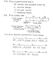
- each message file Fj the names of the sectors S k which compose the message information are stored in the order needed to make up the message. For example, at (a) in Figure 12 we learn that Message Ml is stored in file F 1 . At file area (b) in the same figure we learn that the message is stored in sectors S 0 , S 2 , S 1 , S 4 , ... S k in that order. Using sector area (c), we can then read the message in file F 1 as "MR. SATO CAME BACK FROM AMERICA." The display control information is stored in memory areas indicated by (d), (e) and (f) in Figure 12. Area (d) is a control file area. In it are stored control files F' 1 - F' m . Each control file F'j designates a summary display by means of a control code address T c followed by several character address numbers C X .
- the control code address T c in a control file F'j designates the address of a storage location in a control code area (e).
- the designated location holds the two bit display classification code from Classification Areas 1 and 2 of the message portion signals.
- the two bit classification codes stored in control area (e) designate the various methods for summary displays of the received message information, such as Partial Display (01), Key Word Display (10) or Abbreviated Display (11).
- Each character address number C x in a control file F' j designates the address of a storage location in a character address area (f).
- the designated location holds the 9 bit relative position number of the first character of a word used in the summary display.
- the control files F' j have a one to one correspondence with the message files F j with the same index number j. They are arranged so the control instructions for a summary display of the message information in message file F j are in a corresponding control file number F' j . Moreover, the memory is controlled so that when the message information in a message file F j is deleted, the contents of the corresponding control file F' j are also deleted.
- the two bit display control codes are replaced by control code addresses T c .
- the two bit display control codes themselves could instead be used at the beginning of the control files F ' j instead of the control code addresses T c .
- a Partial Display is a continuous string of words taken from the actual message; it is designated by indicating the first and last words in the string.
- character address C l in character address area ( f ) we find the stored binary number "000 101 001", which is decimal 41 . This means that the first letter of the first word of the partial display begins at character position 41, at the letter "G” of "GO".
- Memory areas (g), (h) and (i) of Figure 12 are set aside as status registers.
- Microprocessor 100 has access to both its internal scratchpad memory RAM 180 ( Figure 7) and the external RAM 300 shown in Figures 5 and 8.
- the main difference between these two RAM memories is that because scratchpad RAM 180 is on the microprocessor chip, it can be accessed faster than external RA M 300 . Therefore, either of these memories could be used to provide the various message and display control memory areas shown in Figure 12.
- the memory areas for the message table (a) and the three registers at (g), (h) and (i) are provided on scratchpad memory 180.
- the three registers are respectively the F-STATUS register, the S-STATUS register, and the C-STATUS register.
- the message file area (b), sector area (c), control file area (d), control code area (e), and character address area (f) will be provided on external memory RAM 300.
- RAM 300 acts as a first memory means for storing received message information.
- RAM 1 80 and the "control data" storing portions of RAM 3 00 will together act as a second memory means for storing control data related to the display of the messages.
- the decoded message portion signals M n contain the 2-bit display control codes of Classification Areas 1 and 2 and the 9 -bit character position indicating numbers of the Control Area. As these arrive, microprocessor 100 refers to the C-STATUS register to learn which character address numbers C x are not yet being used. These available address numbers C x are then stored in the control files F' j of control file area (d) to indicate the addresses where the 9-bit character position indicating numbers are stored. As each C x is used, microprocessor 100 updates the C -STATUS register by putting a "1" in the appropriate bit CS x. The addresses C x used to store the 9-bit character position indicating numbers are located in external RAM 300.
- the decoded message portion signals M n next contain the data of the message information areas. As these arrive, microprocessor 100 refers to the F-STATUS and S-STATUS registers to learn which message files F j and sectors S k are not yet being used. The available sector names are then stored in the available message files F j in the message file area (b) of external RAM 300 to indicate the sectors where a message will be stored. As each sector S k is used to store message information, microprocessor 100 updates the F-STATUS and S-STATUS registers by putting a " 1" in the appropriate bits FSj and SSk.
- Microprocessor 100 transmits the 20 or 21 bits of data in each of the error corrected message portion signals M n to external RAM 3 0 0, where the data is stored for safekeeping. Using Figures 6 and 8, how this is done will now be explained. First, microprocessor 100 outputs a logical "O" at port 113 as a chip enable signal CE to put external RAM 300 in its active mode. Next, microprocessor 100 refers to the F-STATUS, S-STATUS, and C-STATUS registers in its scratchpad RAM 180 to confirm the use condition of the various memory areas in external RAM 3 00 .
- the address information about unused memory areas is transmitted to RAM 300 by a signal SOUT via serial interface 108.
- microprocessor 100 outputs a logical "1" at port 114 to make an A/D (address/data) control signal to RAM 300 designate "address”. It also sends clock timing pulses to RAM 300 as a system clock signal SCK via interface 108.
- RAM 300 of Figure 8 interprets signal SOUT as an address signal.
- the address counter 320 and X-Y decoder 330 in RAM 300 are then used to designate the array addresses in memory array 340 at which display data is written when received.
- microprocessor 100 readies RAM 300 to receive and store output signal SOUT as message and character position data, etc. It switches the A/D signal to "0" for “data” and the R/W signal to "0" for “write”.
- Signal SOUT transmitted via serial interface 108, now carries the message and character position data, etc. to be received and stored by RAM 30 0 .
- RAM 300 In response to the various control signals, RAM 300 writes the data received as signal SOUT in memory array 340 at the previously designated array addresses as message and character position data.
- microprocessor 100 finds that it cannot receive the message signal for two successive words, it outputs an ME (message end) signal at output port 111 to inform address decoder 40 that the message has ended. Whereupon, decoder 40 stops supplying clock signal CL to microprocessor 10o at input port 105. Or alternatively, should decoder 40 be first in detecting an end or stop signal portion E in received signal h, it automatically stops supplying clock signal CL to microprocessor 10 0 .
- ME message end
- microprocessor 100 stops the processing by which it decodes the message signals. At the same time, it outputs an audio control signal AC at output port 112 to control a sound generating circuit in decoder 40.
- a sound generating signal k is applied to the base of NPN transistor 73 0 via input resistor 710.
- the collector output of transistor 73 0 is coupled to the base of PNP transistor 740 by resistor 720.
- signal k drives transistor 730 between conduction and non-conduction, the base voltage of transistor 740 is correspondingly switched between two voltage levels corresponding to logical " 0 " and "1".
- transistor 740 is switched between conduction and non-conduction, regulating the driving current supplied to speaker 80 by battery 1000 which is coupled to the emitter of transistor 740. This causes speaker 80 to produces an audible alarm, informing the user of the paging receiver that he has been paged.
- this type of paging receiver has an automatic alarm cutoff function (auto-reset function) which terminates the paging alarm after a preset period, such as about 8 seconds.
- auto-reset function automatic alarm cutoff function
- the pager's alarm automatically stops after a short timed interval.
- the frequency regulating crystal 41 which is coupled to decoder 40 is part of a crystal oscillator circuit within the decoder.
- the oscillator circuit produces a high frequency signal which is frequency divided to produce a periodic signal f T of about 2kHz. This is supplied to microprocessor 100 at input port 1 0 4 and used as a timing signal. The pager's alarm is terminated after a timed interval of about 8 seconds.
- the user can then select the Summary Display mode X5 by closing switch SW1 (to pass to the Message Display Mode X2) and then closing switch SW3. Closing these switches produces further trigger signals, in accordance with which the microprocessor switches into the summary display function mode of the invention.
- Figure 13 shows a sample flow chart of how a summary display function can be provided by suitable programming of microprocessor 100.
- the summary display function routine begins when the microprocessor is in the Message Display Mode X2 and the user closes operating switch SW3 (Step 1). Then, an index variable i is initially set equal to the number 1 (Step 2a). This prepares microprocessor 100 to begin by processing the most recently received of the stored messages. Next a register S is initially set equal to zero (Step 2b).
- the first character address stored in control file F' j of (d) of Figure 12 is read as C x (Step 4). Then, the current character positior. number PN stored at character address C x is read. The microprocessor uses the position number PN to read out the character at that position in the message that is stored in R AM 300 (Step 5). This character is the first character in the first word of the summary display made from the message.
- the first character address is C 1 .
- the character position table at (f) of Figure 12 shows that the character position number stored at character address Cl is a binary "000 101 001", equivalent to decimal 4 1 . Therefore, the microprocessor will read out from RAM 300 the 41st character in the message of file F 1 . As shown in Figure 4(c), the 41st character in this message is the " G " of "GO".
- the symbol " " is used to represent a blank character in the display.
- the microprocessor's ALU circuit 150 determines if the character which has just been read out is a blank (Step 6). If it is not, the character is loaded in a buffer register (Step 7).
- the character position number PN found at character address C x is increased by one (Step 8).
- the current character position is 41 for the letter “G”..This is increased to position 42, which corresponds to the "O" of "GO”.
- Steps 9, 10, and 11 will detect when the beginning of the last word of the Partial Display has been reached and set an indicating register S.
- the next character address in the control file F' j of (d) of Figure 12 is read as C' x (Step 9).
- the character position number stored at C' x is the position number PN of the first character in the last word of the Partial Display.
- control file F' 1 begins.with code address T 1 for a Partial Display.
- the C' x character address is C3 .
- the character position number stored at character address C 3 is a binary "000 101 111", equivalent to decimal 47. Therefore, the 47th character in the message file F 1 is the first character of the last word of the Partial Display. (As shown in Figure 4 (c), this character is the "N" of "NARITA".)
- Step 10 The current position number PN stored at character address C x is compared with the position number stored at character address C' x (Step 10). If they are equal, a register S in scratchpad RAM 180 which was initially at "0" is set to "1" for use later at Step 13 (Step 11). Otherwise, the microprocessor loops back to Step 5 to read out the next character in the message stored in RAM 300.
- the current character position number PN stored at character address C x was increased to 42 at Step 8. Since 42 does not equal the position number 47 stored at character address C3, the microprocessor loops back to Step 5 to read out the letter "O" stored at character position number 42.
- Step 6 After each additional character for the summary display is read out at Step 5, it is checked to see if it is a blank (Step 6). A blank indicates the end of the current word the characters of which are being processed.
- control code address T c in control file F' j is used to determine if the summary display is coded for a Partial Display (Step 12).
- Register S is read to see if its contents are 1 (Step 13).
- a 1 in register S means that all the characters to be used in the Partial Display have been loaded into the buffer register. Therefore, the microprocessor now sends these characters to LCD Driver 200 to have them displayed by LCD display 90 (Step 20).
- a 0 in register S means that there are further words for the Partial Display not yet loaded. Therefore, there is a jump back to Step 7 to continue loading characters for the display into the buffer register.
- Step 12 the control code address T c in control file F'j is used to determine if the summary display is coded for an Abbreviated Display (Step 14). If it is, PROM 50 is checked to see if the word just ended by the space detected at Step 6 has a prestored abbreviation message (Step 15 ). If it does, the abbreviation message is substituted for the word in the buffer register (Step 16). Otherwise, there is no substitution, and the microprocessor moves on to Step 1 7 .
- Step 17 the control code address T c in control file F'j indicates that the summary display is coded for a Key Word Display.
- the next character address in the control file F' j of (d) of Figure 12 is read as C' x (Step 17). If character address C' x is 0, there are no more words for the Abbreviated or Key Word Display (Step 18).
- the characters for the summary display are sent by the microprocessor for display by the display means in the same way that the full message data stored in external RAM 300 is sent and displayed.
- a "Message Type Display” indicating the message topic or class may be needed. Or it may be desired to select key words from a message but change-their order of appearance for the Key Word Display, etc.
- the 00 code of Classification Area of Figure 4(a) could be used to indicate such further displays, and the number of bits in Classification Area 2 expanded to provide the necessary additional codes.
- the received paging signals have control codes preceding the message information.
- the control codes enable only the principal items which tell the gist of the messages to be selected from the message contents. These appear in a summary display that fits within the limited display area of the display panel.
- summary displays such as Partial Display, Key Word Display, Abbreviated Display, and Message Type Display, can be provided.
- Such summary displays enable the user to quickly grasp the gist of a number of relatively long received messages without having to repeatedly scroll the display to read through each message in its entirety.
Abstract
Description
- This invention relates to a portable paging device for enabling a user to receive a paging message transmitted to him from another location, and more particularly to a selective paging receiver with a message display capable of reading out received message data and selecting the type of control used to show it to the user by means of the display.
- Radio receivers for paging that include a message display panel conventionally scroll the message contents in a limited display area or display window to report the message to the person who has the receiver. That is, when the user presses a switch, all or a portion of the message information is shown to him in the limited message display area, character by character, and in an order beginning with the first character.
- However, someone using a paging receiver with such a scrolling display will soon discover that it takes a considerable amount of scrolling to read a received message. For example, if the message display area can only show 16 characters at a time and if the received message is 350 characters long, the scrolling area will have to be used at least 22 times to deliver the full message. Obviously, such scrolling is even more inconvenient when the user wishes to read several individual messages received and stored by the paging receiver over a period of time.
- For quickly scanning through multiple messages, some paging receivers have a "truncated display" function that permits just the first few characters of each message to be scrolled, rather than all of the characters of each message. Unfortunately, scanning through only such initial portions of the messages is often ineffective in helping the reader grasp their contents and importance.
- Therefore, an object of the invention is to provide a selective paging receiver that enables the user to grasp the information in long messages without scrolling through their entire contents. A more particular object is to provide a paging receiver with a display having a "summary display function", by which is meant the ability to indicate the contents of received messages by a partial display, key word display, abbreviated display, or message type display. Yet a further object is to provide this summary display function within the limited area of the display used for messages, without increasing the number of character positions in the message display area.
- In keeping with one aspect of the invention, a pager has a receiver for receiving selective paging numbers and message data. A message display panel displays paging messages to the user. For storing message data, the pager has a first memory means. Control data, arriving together with the message data and related to its display, is stored in a second memory means. A display controller, responsive to external operating inputs from the user, is provided for controlling the contents of the messages to be displayed based on the control data. A display means responds to control from the display controller, to read out and display messages stored in the first memory means.
- The above mentioned and other features of this invention and the manner of obtaining them will become more apparent, and the invention itself will be best understood, by reference to the following description of an embodiment of the invention taken in conjunction with the accompanying drawings, in which:
- Figure l(a) shows the digital make-up of a typical paging signal received by a receiver according to the invention;
- Figure l(b) shows the digital make-up of address and message portion signals included in the paging signal of Figure l(a);
- Figure 2 is a simplified block diagram of an inventive selective paging receiver with message display for receiving the signals of Figure 1;
- Figure 3 is a flow chart showing the operation of the address decoder in the receiver of Figure 2;
- Figure 4 (a) shows the codes used in a Classification Area 1 of a first message portion signal of Figure l(b);
- Figure 4(b) shows the codes used in a Control Area of the message portion signals of Figure l(b);
- Figure 4(c) shows a sample message signal, received by the receiver of Figure 2;
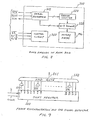
- Figure 5 is a block diagram of the message data processing circuit in the receiver of Figure 2;
- Figure 6 is a block diagram of the one chip CPU or microprocessor in the processing circuit of Figure 5;
- Figure 7 is a block diagram of the LCD driver circuit in the processing circuit of Figure 5, and its associated LCD display;
- Figure 8 is a block diagram of the random access memory (RAM) in the processing circuit of Figure 5;
- Figure 9 is a block diagram of a detector circuit, for detecting certain frame and stop signals, used by the address decoder in the receiver of Figure 2;
- Figure 10 is a simplified schematic of a detecting circuit, for detecting selective paging signals, used by the address decoder in the receiver of Figure 2;
- Figure 11 is a simplified schematic of the buffer amplifier and paging speaker circuits in the receiver of Figure 2;
- Figure 12 is an explanatory chart of the various memory storage areas (a) - (i) provided for message and control information;
- Figure 13 is a sample flow chart showing how a summary display function can be provided by the receiver of Figure 2; and
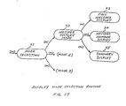
- Figure 14 is an illustration of a routine by which the pager's various types of displays can be selected using operating switches.
- The inventive selective paging receiver receives paging signals by means of its radio receiver section. If the paging number in the signal is the receiver's own identification number, it then receives and decodes control data and message data from the paging signal
- The message data is stored in a first memory means and the control data is stored in a second memory means. The received control data is for controlling a display, in a limited area of a display panel, which helps the user to grasp the received message information. In addition to full message displays, the received control data includes information enabling a brief summary display of each received message.
- For example, the control data can be for controlling various helpful summary displays, such as a partial display, a key word display, an abbreviated display, or a message type display. A "partial display" comprises salient parts of a lengthy received message likely to convey its gist. A "key word display" attempts to report the principal information in a message by displaying a number of its key words. An "abbreviated display" employs prestored abbreviations of the words used in the partial and key word displays so a message of many words can be displayed in compressed form. A "message type display" shows to which classified topic the message information belongs; it enables the received message to be understood as "RE: CASE". The person carrying the receiver uses selection buttons or the like to choose the summary display function. This enables the summary displays provided by the sender to appear in the display panel.
- When the user has selected the summary display mode, the display controller, guided by the received control data stored in the second memory means, reads out selected message data stored in the first memory means and outputs it to the display means.
- As explained above, the invention gives the user the option of reviewing various helpful summary displays of paging messages stored in the receiver, such as a partial display, key word display, abbreviated display, or message type display. For convenience, the term "principal items" are used to refer generally to the words or abbreviations used in these summary displays.
- Figure l(a) shows the digital make-up of a typical paging signal received by a receiver according to the invention. These signals are constructed so that the principal items used in the summary displays can be extracted from the message information.
- The paging signal is a format having a 62 bit preamble signal P, a 31 bit frame synchronizing signal SC, a 31 bit address signal A, a message signal M, and a 31 bit end signal E.
- The frame synchronizing signal SC and the end signal E each have a predetermined fixed pattern. The message signal M has a length that depends on the amount of information in the message. As illustrated at Figure l(b), it is made up from as many 31 bit message portion signals Mn (n = 1, 2, ...) as are needed to convey the message.
- The make-up of the address signal A and the message portion signals Mn for Bose-Chandhuri-Hocquenghem BCH (31, 21) binary coded error correcting signals is shown at Figure l(b). Each signal is a 31 bit word comprising a 21 bit Information Area followed by a 10 bit Check Area.
- During processing, the address signal A and the initial message portion signal M1 are distinguished from each other by the leftmost or most significant bit (MSB),
bit # 1, in the Information Area. The MSB is a logical "0" in an address signal and a logical "1" in an initial message portion signal M1. - In the initial message portion signal, the twenty bits of Information Area which follow the MSB have a very important use in this invention. This is the area which makes it possible to extract the "principal items" used in the various summary displays. It indicates the particular-method of summary display for each message and the extraction points in the message.
- Following the MSB is
Classification Area 1, comprised of two bits,bits # 2 & 3, which designate the form of summary display that will appear in the limited display area used for messages. Next isControl Area 1 which designates the extraction points. - Figure 2 shows a simplified block diagram of an embodiment of the invention, a selective paging receiver with message display for receiving and using the paging signals of Figures l(a) and (b). Electromagnetic signal waves picked up by an
antenna 10 are fed to aradio receiver section 20, which recovers the baseband paging signal and sends it to a waveshape adjusting circuit 30. - From there the paging signal is input to an address decoder 40 having a timing clock the accuracy of which is assured by
crystal 41.Decoder 40 can read out data from a programmable read-only memory (PROM) 50 and exchange data with a messagedata processing circuit 60 via a multi-line signal f. Various information useful for running the receiver, such as its identification number, etc., have been written for storage intoPROM 50, a memory device which can be programmed with information (written into) once, but not reprogrammed. - The output from
decoder 40 is fed to aspeaker 80 via an isolatingbuffer amplifier 70. Processed message data fromcircuit 60 is output to liquid crystal display (LCD)device 90 for displaying message information, etc. to the user. Operating switches SWO, SW1, SW2, SW3 enable the user to turn off an audible speaker alarm, to select operation and display modes, etc. - The detailed operation of this selective paging receiver with message display will now be described.
- When the desired radio signal is picked up by
antenna 10 and recovered byradio receiver section 20, its waveform is shaped bycircuit 30 into a serial digital paging signal h, of the type shown at Figure l(a). Signal h is input to addressdecoder 40. -
Decoder 40 gets into bit synchronization using the preamble signal P, which has a repeating pattern of logical l's and 0's, and proceeds to detection of the frame synchronizing signal SC which comes right after it.' - Figure 3 is a flow chart showing the operation of the
address decoder 40 in the receiver of Figure 2. With power on, when detection of the frame synchronizing signal SC is confirmed,decoder 40 reads out its prestored selective paging address from PROM 50 and starts comparing it bit by bit with received address signal A, the next item in digital signal h. If the receiver's address matches the one in the paging signal,decoder 40 activates messagedata processing circuit 60 by means of signal f. - Immediately thereafter, message signal M is received and its 21 information bits are error corrected by using the 10 check bits. At the same time,
decoder 40 begins watching for an end or stop signal E portion in digital signal h. When an end signal E is detected, thedecoder 40 loops back to wait for detection of the next frame synchronizing signal SC. - Figures 4(a) and (b) show an example of the make-up of the
Classification Area 1 and Control Area appearing in the message signal of Figure l(b). - As stated earlier,
Classification Area 1 comprises two bits which designate the form of display that will appear in the limited display area used for messages. The Control Area designates the positions of the first characters of words to be displayed. Nine bits are used to designate the position of each such character. Therefore, its relative position can be as far away as the 512th position. - Next, using the sample message shown at Figure 4(c), examples will be given of the various methods of summary display.
- When the two
bit Classification Area 1 of initial message portion signal M1 is "00", it indicates that the next message portion signal M1's Information Area will also be a Control Area. Then, in initial message portion signal M1 several of the bits which immediately followClassification Area 1 are used as a further classification area,Classification Area 2, for enabling the method of display to be designated in more detail. This is explained more thoroughly below in connection with the expanded control area. - When the two
bit Classification Area 1 is "01", a partial display is designated. In the Control Area that follows, the next nine bits indicate the position of the first character of the first word used in the partial display, and the remaining nine bits indicate the position of the first character of the last word in the partial- display. For example, the Control Area might designate the string of bits "000101001000101111" . - For convenience, let us follow the convention of grouping these long bit strings by threes, viz: "000 101 001 000 101 111". The first nine bits (000 101 001) have the
decimal value 41. From the sample message in Figure 4(c), this means that the first letter of the first word of the partial display begins atcharacter position 41, at the letter "G" of "GO". The remaining nine bits (000 101 111) have the decimal value 47. This means that the first letter of the last word of the partial display begins at position 47, at the letter "N" of "NARITA". Therefore, the sample message information is shrunk for the partial display to "GO TO NARITA". - When the two
bit Classification Area 1 is "10", a key word display is indicated. In the Control Area that follows, each group of nine bits indicates the position of the first character of a word to be extracted from the message for the key word display. - For example, suppose that the Control Area designates the bits "000 000 101 000 101 111". The first nine bits (000 000 101) have the
decimal value 5. From the sample message in Figure 4(c), this means that the first letter of the first key word begins atcharacter position 5, that is, at the "S" of "SATO". The next nine bits (000 101 111) have the decimal value 47. This means that the first letter of the next key word begins at position 47, at the letter "N" of "NARITA". Therefore, the sample message information is reduced to the words "SATO NARITA" in the keyword display. - When the two
bit Classification Area 1 is "11", an abbreviated display is indicated. In the Control Area that follows, each group of nine bits indicates the position of the first character of a word to be used in the abbreviated display, in a prestored abbreviation form if possible. The abbreviations that can be used in the display are prestored inPROM 50. - For example, suppose that the Control Area designates the bits "000 000 101 000 110 110". The first nine bits (000 000 101) have the
decimal value 5. From the sample message in Figure 4(c), this means that the first letter of the first word for the abbreviated display begins atcharacter position 5, that is, at the "S" of "SATO". Therefore, a comparison is performed to see if an abbreviation for "SATO" is stored inPROM 50. If no prestored abbreviation exists, the word indicated is used as is. Let us assume that on checkingPROM 50, it is found that "SATO" has no prestored abbreviation. If so, it is used in the abbreviated display as is. - The next nine bits (000 110 110) have the decimal value 54. This means that the first letter of the next word for the abbreviated display begins at position 54, at the letter "A" of "AIRPORT". Let us assume that on checking
PROM 50, it is found that "AIRPORT" has a prestored abbreviation of "A. P.". If so, in the abbreviated display "A. P." is used in place of the word "AIRPORT". - Therefore, the sample message information is reduced to the expression "SATO A. P."in the abbreviated display.
- As illustrated above, the two bits of
Classification Area 1 are used to designate the type of summary display. WhenClassification Area 1 is "10" (Key Word Display) or "11" (Abbreviated Display), as shown at Figure 4(b) ii) only two nine bit "position-indicating" numbers can be stored in the control area. Therefore, the Key Word or Abbreviated display is limited to just two words or abbreviations, and not all the display area is used effectively. - If
Classification Area 1 is instead designated as "00", as shown at Figure 4(b) i), the Control Area is expanded by continuing it into the 21 bit Information Area of message portion signal M2. Then, in the initial message portion signal M1 a further classification area (Classification Area 2) is provided directly behindClassification Area 1, to enable a more detailed Key Word or Abbreviated display. - For example, if
Classification Area 2 is two bits long (bits #4 & 5), we can use the same classification codes for it that were used in Classification Area 1: - 01 = Partial Display
- 10 = Key Word Display
- 11 = Abbreviated Display
- For a Key Word display, the two bits of
Classification Area 2 are "10", and for an Abbreviated display the two bits are "11". SinceClassification Area 2 is assumed to take only two bits, as shown at Figure 4(b) i) there is still room in initial message portion signal M1 for a 16 bit Control Area at bits #6 - 21. In addition, becauseClassification Area 1 is "00", the Control Area continues to the next message portion signal M2, where there is room for another 21 control bits (bits #1 - 21). - Therefore, there is a total of 37 (16 + 21) control bits to designate a plurality of (9 bit) position-indicating numbers for the Key Word or Abbreviated display. At a 9 bits per position designation, a total of four (4 X 9 = 36 < 37) Key Words or Abbreviations can be designated. As before, each word is designated by giving the relative position in the message of its first character.
- In the embodiment disclosed above, as shown at Figure 4(a),
Classification Area 1 designates a two bit code indicating the type of summary display. However, with suitablemodifications Classification Area 1 can instead designate a code, extracted from the key words of long sentences, for making certain preselected sentences. - For example, consider paging those doing business in a market where there is frequent dealing in stock prices, etc. Key words can be extracted from the stock names and forecasts in a series of paging message information that reports stock names, prices, and forecasts of future-fluctuations. Then
Classification Area 1 can designate a code which indicates how to use the key words to form such summary displays such as "NEC -- BUY", "ABC -- SELL". When the user wants to learn more about these matters, he can also scroll the message information in its entirety to learn the specific details of stock prices, etc. - The mechanism by which words are designated for the display will now be explained, including the message
data processing circuit 60 and liquid crystal display (LCD) 90. - Figure 5 is a block diagram of the message
data processing circuit 60 in the receiver of Figure 2. - As shown in Figure 5, processing
circuit 60 receives the user's operating instructions by reading input lines from user operating switches SW1, SW2, SW3 (Figure 2), receives input fromaddress decoder 40 on line f, and outputs display driving signals to the liquid crystal display (LCD)- 90 (Figure 2) on line j. Processingcircuit 60 has a one chip CPU ormicroprocessor 100 that reads and writes data to a random access memory (RAM) 300 on line bl. AnLCD driver 200 receives input about the display contents frommicroprocessor 100 on line b2 and outputs display driving signals on line j. - In Figure 5, VDD indicates a power supply voltage applied from a battery 1000 (Figure 11) through a DC-DC converter (not shown). A power supply back-up
capacitor 62 is provided forRAM 300. Adiode 61 is inserted in the line from the power supply so that if voltage VDD drops below the voltage ofcapacitor 62, the diode will open, isolating the back-up capacitor from the power supply. -
RAM 300 acts as a first memory means for storing received message information, etc. TheLCD driver 200 andLCD display 90 together form a display means for displaying the message information to the user.Microprocessor 100 acts as a display controller means for controlling the display means. - It is convenient if the operating switches SWO, SW1, SW2, and SW3 are normally open push button switches that spring back to the open condition when released. Then the user can press (close) them one or more times in various sequences to give commands to the microprocessor (Figure 14).
- When the user closes operating switch SWO (Figure 2), it results in a trigger signal being input from
decoder 40 on line f tomicroprocessor 100. The microprocessor responds by entering a Mode Selection state Xl shown in Figure 14. In state X1, switch SW1 enables selection of a Message Display Mode X2, while SW2 and SW3 respectively enable selection ofModes - Assuming SW1 is pressed while in the Mode Selection state Xl, the microprocessor responds by entering the Message Display Mode or state X2. The user can then choose from among a Full Message Display (X3) by SW1, a Message Number Display (X4) by SW2, and a Summary Display (X5) by SW3. (The Message Number Display shows the number of each message so the user will know how many have been received, etc.)
- If desired, the default display mode (when none of switches SW1, SW2, or SW3 is pressed after a short wait) can be a "truncated display", causing
LCD display 90 to display only a preselected number of beginning characters from each of the various messages stored inRAM 300. - If the user selects the Summary Display by closing operating -switch SW3,--
microprocessor 100 causesLCD display 90, to display certain corresponding "principal items" from the messages stored inRAM 300 as a summary display in accordance with control data stored in a second memory means. The second memory means is discussed in more detail below. - Furthermore, there is an easy way for the user to read out all of a message having a summary display which has caught his attention. While the summary display of that message is still being shown by
LCD display 90, the user can again close switch SWO. This causes a trigger signal to be input tomicroprocessor 100 fromdecoder 40 on line f.Microprocessor 100 then returns to the Mode Selection state Xl of Figure 14. If the user next presses switch SW1 twice in succession,microprocessor 100 moves to the Message Display Mode X2 and then continues on into the Full Message Display mode X3. It reads out fromRAM 300 the entire stored message information for the message, displaying it viadisplay 90. - The details of
microprocessor 100,LCD driver 200, andRAM 300 are respectively shown in Figures 6, 7 and 8. - As shown in the block diagram of Figure 6, for input/output,
microprocessor 100 has input ports 101 - 106, aport 107 for interrupts, and aserial interface 108. It also has output ports 111 - 117 and adata bus 120. - A
program memory 140 stores the sequence of program instructions that must be executed. Aprogram counter 130 specifies the address of the next instruction to be read out ofmemory 140 and executed. Aninstruction decoder 160 decodes the program instruction information read out fromprogram memory 140. It then provides control signals in accordance with the instructions to the various circuits for execution of the instructions. An arithmetic/logic unit (ALU) 150 performs arithmetic and logical operations called for by the program instructions. - An accumulator (ACC) 170 is used in sending data to, and receiving it from,
RAM 180 and the various ports 101 - 117. Aninternal RAM 180 is a scratch pad memory for storing various types of data and providing temporary storage for program status information and program counts when executing subroutines and interrupts. A systemclock generator circuit 190 generates a series of timing pulses that determine the instruction execution cycle times. - Figure 7 shows a block diagram of the
LCD driver 200 in the processing circuit of Figure 5, and its associated LCD display 90. TheLCD driver 200 has acolumn driver 210 for controlling the columns shown bydisplay 90, and arow driver 220 for controlling the rows. Adisplay voltage controller 230 controls the voltage supplied to the LCD display, and atiming controller 240 controls timing of the driving signals to the LCD display. - In Figure 7, input line LCD P.S. indicates a power supply line from a battery 1000 (Figure 11). A clock input line CLK supplies a system clock from
system clock generator 190 on-the microprocessor chip 100 (Figure 6). -
Display driver 200 includes adata memory 250 which can store output from acharacter generator circuit 290 or store display data input via aserial interface 295.Circuit 260 is a system clock controller. Acommand decoder 270 takes in and decodes the display instructions input frommicroprocessor 100 viaserial interface 295. It then provides control signals in accordance with the instruction contents to the various circuits for execution of the instructions. - When data from
serial interface 295 is stored, a data pointer 280 holds the address indata memory 250 at which it is to be written. When data is read out fromdata memory 250 intoserial interface 295, data pointer.280 holds the address from which it is to be read. Thecharacter generating circuit 290 generates a 7X 5 dot matrix character pattern in accordance with - data input to it. The
serial interface 295 enablesdisplay driver 200 to receive data in serial form from, and send it to,microprocessor 100. - Figure 8 shows a block diagram of the random access memory (RAM) 300 in the processing circuit of Figure 5. A
serial interface 310 enables RAM-300 to receive data in serial form from, and send it to,microprocessor 100. Anaddress counter 320 receives input pulses viaserial interface 310. - RAM chip 300 includes a
memory array 340 having storage locations which are organized in rows and columns. An X-Y decoder 330 analyzes the data in theaddress counter 320 to designate a corresponding memory array address inmemory array 340. Display data is written into, or read out of, the memory array addresses designated byX-Y decoder 330. Acontrol circuit 350 receives control signals frommicroprocessor 100, such as those controlling the reading and writing of display data. - Figure 9 is a block diagram of a detector circuit, for detecting frame synchronization and stop signals, used by address decoder 40.in the receiver of Figure 2. A 31
bit shift register 500 is provided that receives the 31 bit words of the digital paging signal h as input from waveshape adjusting circuit 30 of Figure 2. A clock pulse is received for timing the shifting of the data in the register. Logical outputs (1's and O's) from the bits stored in the register are input to a multi-input ANDgate 540, preselected input lines to ANDgate 540 havinginverter circuits register bits # - Figure 10 shows a simplified schematic of a detecting circuit, for detecting selective paging signals, used by the
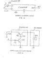
address decoder 40 in the receiver of Figure 2. Acounter 600 receives as input a clock signal and the output of an Exclusive NORgate 610. The inputs to Exclusive NORgate 610 are the digital paging signal h from waveshape adjusting circuit 30 and a signal p fromprogrammable ROM 50. The output of Exclusive NORgate 610 will only be a logical "1" for those bits where its two inputs agree, i.e. bits of signal h that agree with the bits of signal p, prestored inPROM 50. - Figure 11 shows a simplified schematic of an audio alarm, comprising the
buffer amplifier 70 andpaging speaker 80 circuits in the receiver of Figure 2. Inbuffer amplifier 70, the base of anNPN transistor 730 receives, via aninput resistor 710, an input alarm signal k from the output ofaddress.decoder 40 of Figure 2. The emitter oftransistor 730 is grounded, and its collector is coupled via aresistor 720 to the base of a drivingPNP transistor 740, the emitter of which is connected tobattery 1000. The collector output oftransistor 740 drives a horn orspeaker alarm 800 inspeaker circuit 80. - Signal waves picked up by
antenna 10 are demodulated byradio receiver section 20, and the recovered signal is shaped by waveshape adjusting circuit 30 into a serial digital paging signal h, of the type shown at Figure l(a). This is supplied to addressdecoder 40.Address decoder 40 gets into bit synchronization with signal h using the preamble signal portion P shown in Figure l(a). - Next,
decoder 40 proceeds to a detection of the 31 bit frame synchronizing signal SC which follows the preamble signal P. Figure 9 shows a detector circuit used indecoder 40 to detect the frame synchronizing signal SC. Serial digital signal h is input into the low end of a 31bit shift register 500 and shifted toward the right into the register, responsive to clock pulses. Register outputs #1 - 31, corresponding to the bits stored inregister 500, are input into a multi-input ANDgate 540. Certain of the register outputs are inverted before being input to gate 540, as indicated byinverter circuits bits # gate 540 and its inputs are arranged so that when the preselected 31 bit pattern of the frame synchronizing signal SC is input to register 500, all of the inputs to ANDgate 540 are logical 1's, causing it to output a 1 at gate output 541. - Detection of synchronizing signal SC causes
decoder 40 to read the next 31 bits of signal h as the address signal portion A. Received address signal A is compared with the receiver's prestored paging address signal by the detection circuit of Figure 10. The receiver's prestored digital paging address is read out fromPROM 50 as signal p. Signal p is compared, bit by bit, with the address signal A portion of signal h by an Exclusive NORgate 610. - Exclusive NOR
gate 610 only produces a logical 1 as an output to acounter 600 when the corresponding bits in input signals p and h match. Hence, if the received address portion A of signal h matches the receiver's prestored paging address, each of the 31 bit positions will match, and counter 600 will count up to 31. In practice,counter 600 is arranged to output a DET (Address Detected) signal if its count reaches 29 or more. That is, only 29 of the 31 bits of address A need to match the prestored paging address for the receiver to recognize that it is being paged. - A reset signal is provided on the
counter 600 at a reset terminal R, to clear the counter to all 0's after the 31 bits of address A have been compared with the bits of signal h. If a DET signal is output because of a count of 29 bits or more, the DET output signal will precede the clearing of the counter by the reset signal. - Meanwhile, the detector circuit of Figure 9 which was used to detect the frame synchronization signal has begun searching for the end or stop signal portion E, in signal h shown at Figure l(a).
- However, the portion of signal h following detection of the receiver's paging address is usually one or more 31 bit message portion signals Mn (n = 1, 2, ...).
- Therefore, from the microprocessor-based message data processing circuit of Figure 6, when the DET (Address Detected) signal is generated by
counter 600 inaddress decoder 40, it is fed as an interrupt signal tomicroprocessor 100 via interrupt port 107. The interrupt activatesmicroprocessor 100. At the same time,decoder 40 supplies a clock signal CL indicating a transmission speed to inputport 105 of the microprocessor. - Using clock signal CL,
microprocessor 100 reads in a 31 bit message signal D at itsinput port 106 fromdecoder 40. The bits in message signal D are the 31 bits in the received message portion signal Mn currently being processed. - By means of its
instruction decoder 160,microprocessor 100 translates instructions prestored inprogram memory 140 and processes signal D by executing them. That is, after being read in viadata bus 120 andaccumulator ACC 170, message signal D is written inscratchpad memory RAM 180.Unit microprocessor 100 then uses its Arithmetic-Logic Unit ALU 150 to carry out the necessary computations on each of the received 31 bits of message signal D stored inscratchpad memory 180 to recover 21 error-corrected information bits from message signal D. - Next, to be explained is how the various decoded BCH (31, 21) message portion signals Mn are handled in memory after error correction. Figure 12 shows an explanatory chart of the storage areas provided for storing messages and display control information. At (a) in Figure 12 is a message table having addresses Mi (i = 1, 2, ... n) storing the message file numbers Fj of new and old received message information. Initially the
- data at addresses Ml - Mn is all zeros, meaning that no messages are stored.
- Figure 12 shows examples of a file area (b) and a sector area (c) in the memory which are together used to store message information. File names Fl - Fm are assigned to correspond to a message file's position number in the file area of memory. The message information is stored in memory in regularly numbered memory sectors Sk. Each memory sector is of fixed length (e.g. 8 characters) and usually only holds a portion of a message. The sector names So - Sk are-assigned to correspond to the sector's position number in the sector area of memory.
- In each message file Fj, the names of the sectors Sk which compose the message information are stored in the order needed to make up the message. For example, at (a) in Figure 12 we learn that Message Ml is stored in file F1. At file area (b) in the same figure we learn that the message is stored in sectors S0, S2, S1, S4, ... Sk in that order. Using sector area (c), we can then read the message in file F1 as "MR. SATO CAME BACK FROM AMERICA...." The display control information is stored in memory areas indicated by (d), (e) and (f) in Figure 12. Area (d) is a control file area. In it are stored control files F'1 - F'm. Each control file F'j designates a summary display by means of a control code address Tc followed by several character address numbers CX.
- The control code address Tc in a control file F'j designates the address of a storage location in a control code area (e). The designated location holds the two bit display classification code from
Classification Areas - Each character address number Cx in a control file F'j designates the address of a storage location in a character address area (f). The designated location holds the 9 bit relative position number of the first character of a word used in the summary display.
- The control files F'j have a one to one correspondence with the message files Fj with the same index number j. They are arranged so the control instructions for a summary display of the message information in message file Fj are in a corresponding control file number F'j. Moreover, the memory is controlled so that when the message information in a message file Fj is deleted, the contents of the corresponding control file F'j are also deleted.
- In the control files of the present example, the two bit display control codes are replaced by control code addresses Tc. However, the two bit display control codes themselves could instead be used at the beginning of the control files F'j instead of the control code addresses Tc.
- To illustrate how this coding in memory of the summary displays works, recall the previous sample message file Fl which contains sector names that point to the message of shown at Figure 4(c), "MR. SATO CAME BACK FROM AMERICA. PLEASE GO TO-NARITA AIRPORT BY SEVEN". The corresponding control file F'1 designates a summary display by the string "Tl C1 C3 0 0 ".
- Looking at address T1 in control code area (e), we find the display code "01", which stands for a Partial Display. A Partial Display is a continuous string of words taken from the actual message; it is designated by indicating the first and last words in the string.
- Looking at character address Cl in character address area (f), we find the stored binary number "000 101 001", which is decimal 41. This means that the first letter of the first word of the partial display begins at
character position 41, at the letter "G" of "GO". - Looking at character address C3 in character address area (f), we find the stored binary number "000 101 111", which is decimal 47. This means that the first letter of the last word of the partial display begins at position 47, at the letter "N" of "NARITA". Therefore, the Partial Display will read "GO TO NARITA". Since no further character addresses are needed for the Partial Display, the last two items in the control file F'1 are filled with zeros.
- This same example appeared earlier relative to coding of the Classification Area and Control Area of received message portion signals. Now we are seeing the same Partial Display after it is stored in memory for use.
- Memory areas (g), (h) and (i) of Figure 12 are set aside as status registers. An F-STATUS register shown at (g) has m bits FSj (j = 1, 2, ... m) that indicate the current use status of the memory's message file area (b). Each bit FSj stores.an indication as to whether the area of the corresponding message file Fj is being used. Bit FSj is "0" when the area of the corresponding file Fj is not in use, and "1" when the area is in use.
- Similarly, an S-STATUS register shown at (h) has L bits SSk (k = 0, 1, 2, ... L) indicating the current use status of the memory's sector area (c). Bit SSk indicates whether the corresponding sector Sk is being used. A C-STATUS register shown at (i) has Y bits CSx (x = 1, 2, ... Y) indicating the current use status of the memory's character address area (f). Bit CSx indicates the use status of the corresponding character address area Cx.
-
Microprocessor 100 has access to both its internal scratchpad memory RAM 180 (Figure 7) and theexternal RAM 300 shown in Figures 5 and 8. The main difference between these two RAM memories is that becausescratchpad RAM 180 is on the microprocessor chip, it can be accessed faster than external RAM 300. Therefore, either of these memories could be used to provide the various message and display control memory areas shown in Figure 12. However, for convenience of explanation, let us assume that the memory areas for the message table (a) and the three registers at (g), (h) and (i) are provided onscratchpad memory 180. The three registers are respectively the F-STATUS register, the S-STATUS register, and the C-STATUS register. - The message file area (b), sector area (c), control file area (d), control code area (e), and character address area (f) will be provided on
external memory RAM 300. Earlier it was mentioned thatRAM 300 acts as a first memory means for storing received message information. In the example memory configuration, RAM 180 and the "control data" storing portions ofRAM 300 will together act as a second memory means for storing control data related to the display of the messages. - The decoded message portion signals Mn contain the 2-bit display control codes of
Classification Areas microprocessor 100 refers to the C-STATUS register to learn which character address numbers Cx are not yet being used. These available address numbers Cx are then stored in the control files F'j of control file area (d) to indicate the addresses where the 9-bit character position indicating numbers are stored. As each Cx is used,microprocessor 100 updates the C-STATUS register by putting a "1" in the appropriate bit CSx. The addresses Cx used to store the 9-bit character position indicating numbers are located inexternal RAM 300. - The decoded message portion signals Mn next contain the data of the message information areas. As these arrive,
microprocessor 100 refers to the F-STATUS and S-STATUS registers to learn which message files Fj and sectors Sk are not yet being used. The available sector names are then stored in the available message files Fj in the message file area (b) ofexternal RAM 300 to indicate the sectors where a message will be stored. As each sector Sk is used to store message information, microprocessor 100 updates the F-STATUS and S-STATUS registers by putting a "1" in the appropriate bits FSj and SSk. -
Microprocessor 100 transmits the 20 or 21 bits of data in each of the error corrected message portion signals Mn toexternal RAM 300, where the data is stored for safekeeping. Using Figures 6 and 8, how this is done will now be explained. First,microprocessor 100 outputs a logical "O" atport 113 as a chip enable signal CE to putexternal RAM 300 in its active mode. Next,microprocessor 100 refers to the F-STATUS, S-STATUS, and C-STATUS registers in itsscratchpad RAM 180 to confirm the use condition of the various memory areas inexternal RAM 300. - The address information about unused memory areas is transmitted to RAM 300 by a signal SOUT via
serial interface 108. To indicate that signal SOUT contains address information,microprocessor 100 outputs a logical "1" atport 114 to make an A/D (address/data) control signal to RAM 300 designate "address". It also sends clock timing pulses to RAM 300 as a system clock signal SCK viainterface 108. - In accordance with the various control signals (CE, A/D, R/W) input to it ,
RAM 300 of Figure 8 interprets signal SOUT as an address signal. Theaddress counter 320 andX-Y decoder 330 inRAM 300 are then used to designate the array addresses inmemory array 340 at which display data is written when received. - Next,
microprocessor 100 readiesRAM 300 to receive and store output signal SOUT as message and character position data, etc. It switches the A/D signal to "0" for "data" and the R/W signal to "0" for "write". Signal SOUT, transmitted viaserial interface 108, now carries the message and character position data, etc. to be received and stored byRAM 300. - In response to the various control signals,
RAM 300 writes the data received as signal SOUT inmemory array 340 at the previously designated array addresses as message and character position data. - As successive message signals are decoded by the microprocessor, eventually a preselected pattern indicating the end of the message signals is detected among the decoded message data. When
microprocessor 100 finds that it cannot receive the message signal for two successive words, it outputs an ME (message end) signal at output port 111 to informaddress decoder 40 that the message has ended. Whereupon,decoder 40 stops supplying clock signal CL to microprocessor 10o atinput port 105. Or alternatively, should decoder 40 be first in detecting an end or stop signal portion E in received signal h, it automatically stops supplying clock signal CL tomicroprocessor 100. - When it finds that the message has ended,
microprocessor 100 stops the processing by which it decodes the message signals. At the same time, it outputs an audio control signal AC atoutput port 112 to control a sound generating circuit indecoder 40. - In response to control signal AC, as shown in Figure 11, a sound generating signal k is applied to the base of NPN transistor 730 via
input resistor 710. The collector output of transistor 730 is coupled to the base ofPNP transistor 740 byresistor 720. As signal k drivestransistor 730 between conduction and non-conduction, the base voltage oftransistor 740 is correspondingly switched between two voltage levels corresponding to logical "0" and "1". - As a result,
transistor 740 is switched between conduction and non-conduction, regulating the driving current supplied tospeaker 80 bybattery 1000 which is coupled to the emitter oftransistor 740. This causesspeaker 80 to produces an audible alarm, informing the user of the paging receiver that he has been paged. - Typically, this type of paging receiver has an automatic alarm cutoff function (auto-reset function) which terminates the paging alarm after a preset period, such as about 8 seconds. In the present embodiment, also, the pager's alarm automatically stops after a short timed interval.
- The
frequency regulating crystal 41 which is coupled to decoder 40 is part of a crystal oscillator circuit within the decoder. The oscillator circuit produces a high frequency signal which is frequency divided to produce a periodic signal fT of about 2kHz. This is supplied tomicroprocessor 100 atinput port 104 and used as a timing signal. The pager's alarm is terminated after a timed interval of about 8 seconds. - 9 While the alarm is sounding, the user may choose to close operating switch SWO (Figure 2). This causes
address decoder 40 to output a signal R to interruptport 107 ofmicroprocessor 100.Microprocessor 100 then immediately terminates the audio control signal AC which is being sent todecoder 40 atoutput port 112. This cuts off the pager's alarm without waiting for the end of the 8 second interval. - Suppose that a number of paging messages have been received and stored in the pager's memory as described above, and that the paging alarm has been terminated. Now the user can close switch SW0, generating a trigger signal. This causes
decoder 40 to send an interrupt signal R tomicroprocessor 100 via interruptport 107.Microprocessor 100 responds by switching the paging receiver into its Mode Selection state Xl of Figure 14. - The user can then select the Summary Display mode X5 by closing switch SW1 (to pass to the Message Display Mode X2) and then closing switch SW3. Closing these switches produces further trigger signals, in accordance with which the microprocessor switches into the summary display function mode of the invention.
- That is, when several individual messages are stored in
RAM 300, successive closing of switches SWO, SWl, and SW3 puts the paging receiver in its Summary Display function mode. A summary display provided by the sender, such as a Partial display, a Key Word display, etc., is then shown of the stored messages, in order beginning with the most recently received. - Figure 13 shows a sample flow chart of how a summary display function can be provided by suitable programming of
microprocessor 100. - The summary display function routine begins when the microprocessor is in the Message Display Mode X2 and the user closes operating switch SW3 (Step 1). Then, an index variable i is initially set equal to the number 1 (
Step 2a). This preparesmicroprocessor 100 to begin by processing the most recently received of the stored messages. Next a register S is initially set equal to zero (Step 2b). - From the message table of (a) of Figure 12 the microprocessor determines which file name Fj is stored at address Mi. It then calls up the corresponding control file named F'j, which has the same subscript j that appears in file name Fj (Step 3).
- Since
Step 2 has set i = 1, the microprocessor enters the message table of (a) of Figure 12 at address Ml. Address Ml always holds the file name Fi of the most recently received of the stored messages. In the example of (a) of Figure 12, address Ml holds the file name F1, so corresponding control file F'l is called up. - The first character address stored in control file F'j of (d) of Figure 12 is read as Cx (Step 4). Then, the current character positior. number PN stored at character address Cx is read. The microprocessor uses the position number PN to read out the character at that position in the message that is stored in RAM 300 (Step 5). This character is the first character in the first word of the summary display made from the message.
- In the example of (d) of Figure 12, in control file F'1, the first character address is C1. The character position table at (f) of Figure 12 shows that the character position number stored at character address Cl is a binary "000 101 001", equivalent to
decimal 41. Therefore, the microprocessor will read out from RAM 300 the 41st character in the message of file F1. As shown in Figure 4(c), the 41st character in this message is the "G" of "GO". - In the Figures, the symbol "" is used to represent a blank character in the display. The microprocessor's

ALU circuit 150 determines if the character which has just been read out is a blank (Step 6). If it is not, the character is loaded in a buffer register (Step 7). - Then, to indicate the next character for the summary display, the character position number PN found at character address Cx is increased by one (Step 8). In the above example, the current character position is 41 for the letter "G"..This is increased to position 42, which corresponds to the "O" of "GO".
- If the summary display is a Partial Display, Steps 9, 10, and 11 will detect when the beginning of the last word of the Partial Display has been reached and set an indicating register S.
- The next character address in the control file F'j of (d) of Figure 12 is read as C'x (Step 9). For a Partial Display, the character position number stored at C'x is the position number PN of the first character in the last word of the Partial Display. In the example of (d) of Figure 12, control file F'1 begins.with code address T1 for a Partial Display. The C'x character address is C3. The character position number stored at character address C3 is a binary "000 101 111", equivalent to decimal 47. Therefore, the 47th character in the message file F1 is the first character of the last word of the Partial Display. (As shown in Figure 4 (c), this character is the "N" of "NARITA".)
- The current position number PN stored at character address Cx is compared with the position number stored at character address C'x (Step 10). If they are equal, a register S in
scratchpad RAM 180 which was initially at "0" is set to "1" for use later at Step 13 (Step 11). Otherwise, the microprocessor loops back toStep 5 to read out the next character in the message stored inRAM 300. - In the above example, the current character position number PN stored at character address Cx was increased to 42 at
Step 8. Since 42 does not equal the position number 47 stored at character address C3, the microprocessor loops back toStep 5 to read out the letter "O" stored at character position number 42. - As previously mentioned, after each additional character for the summary display is read out at
Step 5, it is checked to see if it is a blank (Step 6). A blank indicates the end of the current word the characters of which are being processed. - If a blank is detected at
Step 5, the control code address Tc in control file F'j is used to determine if the summary display is coded for a Partial Display (Step 12). - If the code is for a Partial Display, Register S is read to see if its contents are 1 (Step 13). A 1 in register S means that all the characters to be used in the Partial Display have been loaded into the buffer register. Therefore, the microprocessor now sends these characters to
LCD Driver 200 to have them displayed by LCD display 90 (Step 20). However, a 0 in register S means that there are further words for the Partial Display not yet loaded. Therefore, there is a jump back toStep 7 to continue loading characters for the display into the buffer register. - If, at
Step 12, a Partial Display is not called for, the control code address Tc in control file F'j is used to determine if the summary display is coded for an Abbreviated Display (Step 14). If it is,PROM 50 is checked to see if the word just ended by the space detected atStep 6 has a prestored abbreviation message (Step 15). If it does, the abbreviation message is substituted for the word in the buffer register (Step 16). Otherwise, there is no substitution, and the microprocessor moves on toStep 17. - The microprocessor will also reach
Step 17 if atStep 14 the control code address Tc in control file F'j indicates that the summary display is coded for a Key Word Display. In either case, an Abbreviated or Key Word Display, the next character address in the control file F'j of (d) of Figure 12 is read as C'x (Step 17). If character address C'x is 0, there are no more words for the Abbreviated or Key Word Display (Step 18). - This also means that all the characters to be used in the Abbreviated or Partial Display have been loaded into the buffer. register. Therefore, the microprocessor now sends these characters to
LCD Driver 200 to have them displayed byLCD display 90 as summary messages that fit within its limited; display area. - Except that they come from the buffer register, the characters for the summary display are sent by the microprocessor for display by the display means in the same way that the full message data stored in
external RAM 300 is sent and displayed. - Assuming that there are n messages to be displayed by summary display, a check is made to see if index variable i = n (Step 21). If it does not, index variable i is increased by 1 (Step 22) and a return is made to Step 2b to make a summary display of the next message. When all n messages have been displayed, i = n (Step 21) and the summary display routine ends.
- The flow chart of Figure 13-illustrates a technique by.which various summary displays, such as Partial Displays, Key Word Displays, and Abbreviated Displays can be provided.
- However, should other types of summary displays be desired, they can be provided. For example, a "Message Type Display" indicating the message topic or class may be needed. Or it may be desired to select key words from a message but change-their order of appearance for the Key Word Display, etc. The 00 code of Classification Area of Figure 4(a) could be used to indicate such further displays, and the number of bits in Classification Area 2 expanded to provide the necessary additional codes.
- In a selective paging receiver having the above described construction and operation, the received paging signals have control codes preceding the message information. The control codes enable only the principal items which tell the gist of the messages to be selected from the message contents. These appear in a summary display that fits within the limited display area of the display panel.
- In practice, various summary displays, such as Partial Display, Key Word Display, Abbreviated Display, and Message Type Display, can be provided. Such summary displays enable the user to quickly grasp the gist of a number of relatively long received messages without having to repeatedly scroll the display to read through each message in its entirety.
- Those who are skilled in the art will readily perceive how to modify the invention. Therefore, the appended claims are to be construed to cover all equivalent structures which fall within the true scope and spirit of the invention.
Claims (12)
Applications Claiming Priority (2)
| Application Number | Priority Date | Filing Date | Title |
|---|---|---|---|
| JP204912/85 | 1985-09-17 | ||
| JP60204912A JPH0669163B2 (en) | 1985-09-17 | 1985-09-17 | Wireless selective call receiver with display function |
Publications (3)
| Publication Number | Publication Date |
|---|---|
| EP0218936A2 true EP0218936A2 (en) | 1987-04-22 |
| EP0218936A3 EP0218936A3 (en) | 1988-09-14 |
| EP0218936B1 EP0218936B1 (en) | 1993-08-04 |
Family
ID=16498437
Family Applications (1)
| Application Number | Title | Priority Date | Filing Date |
|---|---|---|---|
| EP86112784A Expired - Lifetime EP0218936B1 (en) | 1985-09-17 | 1986-09-16 | Selective paging receiver with message display |
Country Status (7)
| Country | Link |
|---|---|
| US (1) | US4766434A (en) |
| EP (1) | EP0218936B1 (en) |
| JP (1) | JPH0669163B2 (en) |
| AU (1) | AU584557B2 (en) |
| CA (1) | CA1259377A (en) |
| DE (1) | DE3688819T2 (en) |
| HK (1) | HK140393A (en) |
Cited By (10)
| Publication number | Priority date | Publication date | Assignee | Title |
|---|---|---|---|---|
| EP0275165A2 (en) * | 1987-01-13 | 1988-07-20 | Nec Corporation | Selective calling radio display pager |
| EP0373176A1 (en) * | 1987-08-05 | 1990-06-20 | Motorola Inc | Paging receiver with dynamically allocated display rate. |
| EP0488104A2 (en) * | 1990-11-26 | 1992-06-03 | Nec Corporation | Radio communication apparatus capable of preventing miss display operation |
| EP0712100A1 (en) * | 1994-11-11 | 1996-05-15 | Casio Computer Company Limited | Receiving terminal with a message display function |
| EP0748134A2 (en) * | 1995-06-06 | 1996-12-11 | Nec Corporation | Radio selective calling receiver with message display capability |
| WO1997037447A1 (en) * | 1996-03-29 | 1997-10-09 | Casio Computer Co., Ltd. | Paging service using broadcasting |
| WO1997039540A1 (en) * | 1996-04-12 | 1997-10-23 | Casio Computer Co., Ltd. | Broadcasting system |
| EP0810566A2 (en) * | 1996-05-28 | 1997-12-03 | Nec Corporation | Data display radio pager |
| GB2320164A (en) * | 1996-11-05 | 1998-06-10 | Nec Corp | Restricting a function of a radio communication device in a specific area |
| US5801640A (en) * | 1992-01-17 | 1998-09-01 | Nec Corporation | Radio pager with a message processing function |
Families Citing this family (45)
| Publication number | Priority date | Publication date | Assignee | Title |
|---|---|---|---|---|
| JPH0624335B2 (en) * | 1987-02-27 | 1994-03-30 | 日本電気株式会社 | Selective call receiver with display |
| EP0308132B1 (en) * | 1987-09-14 | 1994-06-08 | Nec Corporation | Paging receiver with a display function |
| JP3159121B2 (en) * | 1987-09-30 | 2001-04-23 | カシオ計算機株式会社 | Information receiver |
| DE68922337T2 (en) * | 1988-05-17 | 1995-08-31 | Casio Computer Co Ltd | Paging communication system. |
| US5032835A (en) * | 1989-04-24 | 1991-07-16 | Motorola, Inc. | Out of range indication for radio receivers |
| US5218629A (en) * | 1989-05-12 | 1993-06-08 | Public Access Cellular Telephone, Inc. | Communication system for message display onboard mass transit vehicles |
| WO1991003040A1 (en) * | 1989-08-14 | 1991-03-07 | Motorola, Inc. | Ideographical character signalling system |
| US5223831A (en) * | 1989-08-14 | 1993-06-29 | Motorola, Inc. | Ideographical character signalling system |
| US5258739A (en) * | 1989-11-09 | 1993-11-02 | Motorola, Inc. | Efficient message storage within a selective call receiver |
| AU6638890A (en) * | 1989-11-09 | 1991-06-13 | Motorola, Inc. | Efficient message storage within a selective call receiver |
| US5146216A (en) * | 1989-12-14 | 1992-09-08 | Motorola, Inc. | Multiple message signalling protocol for a selective call receiver |
| US5283570A (en) * | 1989-12-14 | 1994-02-01 | Motorola, Inc. | Multiple format signalling protocol for a selective call receiver |
| US5323148A (en) * | 1991-02-28 | 1994-06-21 | Motorola, Inc. | Selective call receiver presenting the length of an alphanumeric message prior to presentation of the message |
| US5272465A (en) * | 1991-11-13 | 1993-12-21 | Telemessaging Devices, Inc. | Automatic alarm code converter |
| WO1993022882A1 (en) * | 1992-05-04 | 1993-11-11 | Motorola, Inc. | Receiver and method for presenting type of message |
| EP0583064B1 (en) * | 1992-07-09 | 1999-05-19 | Nec Corporation | Radio paging receiver with display unit |
| CA2145874C (en) * | 1992-09-30 | 1999-09-21 | John Richard Kane | Electronic mail message delivery system |
| US5495234A (en) * | 1993-01-21 | 1996-02-27 | Motorola, Inc. | Method and apparatus for length dependent selective call message handling |
| EP0660281A1 (en) * | 1993-12-24 | 1995-06-28 | Nec Corporation | Radio communication device combinable with a radio modem for computer |
| US7266186B1 (en) | 1994-01-05 | 2007-09-04 | Intellect Wireless Inc. | Method and apparatus for improved paging receiver and system |
| US6278862B1 (en) | 1994-01-05 | 2001-08-21 | Daniel A. Henderson | Method and apparatus for enhancing the efficient communication of information in an alphanumeric paging network |
| US6427064B1 (en) | 1994-01-05 | 2002-07-30 | Daniel A. Henderson | Method and apparatus for maintaining a database in a portable communication device |
| US7426264B1 (en) | 1994-01-05 | 2008-09-16 | Henderson Daniel A | Method and apparatus for improved personal communication devices and systems |
| US5539529A (en) * | 1994-04-04 | 1996-07-23 | Merchant; Zaffer S. | Facsimile communication with selective call receivers |
| KR0165210B1 (en) * | 1995-06-26 | 1999-02-01 | 김광호 | Apparatus and method of voice paging of wireless paging receiver |
| JP2957445B2 (en) * | 1995-08-21 | 1999-10-04 | 静岡日本電気株式会社 | Radio selective call receiver |
| JP2702463B2 (en) * | 1995-11-13 | 1998-01-21 | 静岡日本電気株式会社 | Radio selective call receiver |
| JP3497028B2 (en) * | 1995-11-17 | 2004-02-16 | 松下電器産業株式会社 | Message notification system, message notification method, and message receiving terminal |
| DE19610493C2 (en) * | 1996-03-18 | 1998-07-30 | Deutsche Telekom Mobil | Process for the dissemination of value added information |
| JP2919393B2 (en) * | 1996-10-29 | 1999-07-12 | 静岡日本電気株式会社 | Call control device and call control method using password |
| JP2972632B2 (en) * | 1997-03-26 | 1999-11-08 | 静岡日本電気株式会社 | Radio selective call receiver |
| JP3071716B2 (en) * | 1997-04-24 | 2000-07-31 | 静岡日本電気株式会社 | Information receiving device |
| US5936547A (en) * | 1997-07-15 | 1999-08-10 | Ameritech Corporation | System and method for providing user-selected information to a paging-capable device |
| US6233430B1 (en) * | 1997-09-19 | 2001-05-15 | Richard J. Helferich | Paging transceivers and methods for selectively retrieving messages |
| US6060997A (en) * | 1997-10-27 | 2000-05-09 | Motorola, Inc. | Selective call device and method for providing a stream of information |
| JPH11266472A (en) * | 1998-03-18 | 1999-09-28 | Nec Shizuoka Ltd | Selective calling radio receiver with display function |
| JP3226164B2 (en) * | 1998-11-06 | 2001-11-05 | 日本電気株式会社 | Mobile personal digital assistant and data display method thereof |
| US6260060B1 (en) * | 1998-11-13 | 2001-07-10 | Motorola Inc. | Method and apparatus for enhancing a message preview mode in a messaging unit |
| DE19861323B4 (en) * | 1998-12-08 | 2006-02-16 | Robert Bosch Gmbh | Method for transmitting short messages |
| EP1052839B1 (en) | 1999-05-13 | 2008-08-06 | Matsushita Electric Industrial Co., Ltd. | Terminal for mobile communication that can display text by switching between different character sets |
| JP2001028788A (en) * | 1999-05-13 | 2001-01-30 | Matsushita Electric Ind Co Ltd | Mobile communication terminal |
| US6993049B2 (en) * | 2000-06-26 | 2006-01-31 | Koninklijke Philips Electronics N.V. | Communication system |
| JP2003269969A (en) | 2002-03-13 | 2003-09-25 | Sony Corp | Navigation device, and spot information display method and program |
| JP5219664B2 (en) * | 2008-07-14 | 2013-06-26 | キヤノン株式会社 | Display device, image forming apparatus, display method, and program |
| JPWO2010113453A1 (en) * | 2009-04-02 | 2012-10-04 | パナソニック株式会社 | Wireless transmission / reception circuit, wireless communication device, and wireless transmission / reception method |
Citations (4)
| Publication number | Priority date | Publication date | Assignee | Title |
|---|---|---|---|---|
| GB2062320A (en) * | 1979-11-01 | 1981-05-20 | Nippon Electric Co | Paging receiver with dispaly |
| WO1982002975A1 (en) * | 1981-02-26 | 1982-09-02 | Gen Electric | Multi-format data display apparatus |
| EP0091691A2 (en) * | 1982-04-13 | 1983-10-19 | Nec Corporation | Radio paging receiver operable on a word-scrolling basis |
| GB2128004A (en) * | 1982-08-27 | 1984-04-18 | Nec Corp | Display radio paging receiver for variable length messages |
Family Cites Families (8)
| Publication number | Priority date | Publication date | Assignee | Title |
|---|---|---|---|---|
| US3757037A (en) * | 1972-02-02 | 1973-09-04 | N Bialek | Video image retrieval catalog system |
| US3976995A (en) * | 1975-05-22 | 1976-08-24 | Sanders Associates, Inc. | Precessing display pager |
| US4336524A (en) * | 1979-07-17 | 1982-06-22 | Levine Alfred B | Video display pager receiver with memory |
| US4385295A (en) * | 1981-09-29 | 1983-05-24 | Motorola, Inc. | Pager with visible display indicating unread messages |
| DE3209187C2 (en) * | 1982-03-13 | 1985-01-10 | Triumph-Adler Aktiengesellschaft für Büro- und Informationstechnik, 8500 Nürnberg | Method for displaying a text on a single-line display device of a text creation device |
| GB2124419B (en) * | 1982-05-31 | 1985-09-18 | Nec Corp | Radio paging apparatus |
| JPS58209238A (en) * | 1982-05-31 | 1983-12-06 | Nec Corp | Radio individual selecting and calling receiver provided with receiving function of message information |
| EP0136677B1 (en) * | 1983-09-30 | 1990-08-16 | Nec Corporation | Multifunctional pager receiver capable of reducing the number of manual switches |
-
1985
- 1985-09-17 JP JP60204912A patent/JPH0669163B2/en not_active Expired - Fee Related
-
1986
- 1986-09-11 US US06/906,148 patent/US4766434A/en not_active Expired - Lifetime
- 1986-09-16 EP EP86112784A patent/EP0218936B1/en not_active Expired - Lifetime
- 1986-09-16 DE DE86112784T patent/DE3688819T2/en not_active Expired - Fee Related
- 1986-09-16 CA CA000518236A patent/CA1259377A/en not_active Expired
- 1986-09-17 AU AU62766/86A patent/AU584557B2/en not_active Ceased
-
1993
- 1993-12-23 HK HK1403/93A patent/HK140393A/en not_active IP Right Cessation
Patent Citations (4)
| Publication number | Priority date | Publication date | Assignee | Title |
|---|---|---|---|---|
| GB2062320A (en) * | 1979-11-01 | 1981-05-20 | Nippon Electric Co | Paging receiver with dispaly |
| WO1982002975A1 (en) * | 1981-02-26 | 1982-09-02 | Gen Electric | Multi-format data display apparatus |
| EP0091691A2 (en) * | 1982-04-13 | 1983-10-19 | Nec Corporation | Radio paging receiver operable on a word-scrolling basis |
| GB2128004A (en) * | 1982-08-27 | 1984-04-18 | Nec Corp | Display radio paging receiver for variable length messages |
Cited By (20)
| Publication number | Priority date | Publication date | Assignee | Title |
|---|---|---|---|---|
| EP0275165A2 (en) * | 1987-01-13 | 1988-07-20 | Nec Corporation | Selective calling radio display pager |
| EP0275165A3 (en) * | 1987-01-13 | 1990-07-04 | Nec Corporation | Selective calling radio display pager |
| EP0373176A1 (en) * | 1987-08-05 | 1990-06-20 | Motorola Inc | Paging receiver with dynamically allocated display rate. |
| EP0373176A4 (en) * | 1987-08-05 | 1991-06-19 | Motorola, Inc. | Paging receiver with dynamically allocated display rate |
| EP0488104A2 (en) * | 1990-11-26 | 1992-06-03 | Nec Corporation | Radio communication apparatus capable of preventing miss display operation |
| EP0488104A3 (en) * | 1990-11-26 | 1993-03-31 | Nec Corporation | Radio communication apparatus capable of preventing miss display operation |
| US5801640A (en) * | 1992-01-17 | 1998-09-01 | Nec Corporation | Radio pager with a message processing function |
| US5966113A (en) * | 1994-11-11 | 1999-10-12 | Casio Computer Co., Ltd. | Receiving terminal with a message display function |
| EP0712100A1 (en) * | 1994-11-11 | 1996-05-15 | Casio Computer Company Limited | Receiving terminal with a message display function |
| EP0748134A3 (en) * | 1995-06-06 | 1998-03-18 | Nec Corporation | Radio selective calling receiver with message display capability |
| EP0748134A2 (en) * | 1995-06-06 | 1996-12-11 | Nec Corporation | Radio selective calling receiver with message display capability |
| US5774061A (en) * | 1995-06-06 | 1998-06-30 | Nec Corporation | Radio selective calling receiver with message display capability |
| WO1997037447A1 (en) * | 1996-03-29 | 1997-10-09 | Casio Computer Co., Ltd. | Paging service using broadcasting |
| WO1997039540A1 (en) * | 1996-04-12 | 1997-10-23 | Casio Computer Co., Ltd. | Broadcasting system |
| EP0810566A2 (en) * | 1996-05-28 | 1997-12-03 | Nec Corporation | Data display radio pager |
| EP0810566A3 (en) * | 1996-05-28 | 1998-06-03 | Nec Corporation | Data display radio pager |
| US6191702B1 (en) | 1996-05-28 | 2001-02-20 | Nec Corporation | Data display radio pager |
| GB2320164A (en) * | 1996-11-05 | 1998-06-10 | Nec Corp | Restricting a function of a radio communication device in a specific area |
| US6131045A (en) * | 1996-11-05 | 2000-10-10 | Nec Corporation | Radio communication device for restricting specific function and method for restricting the function |
| GB2320164B (en) * | 1996-11-05 | 1999-07-07 | Nec Corp | Radio communication device for restricting specific function and method for restricting the function |
Also Published As
| Publication number | Publication date |
|---|---|
| AU584557B2 (en) | 1989-05-25 |
| US4766434A (en) | 1988-08-23 |
| EP0218936B1 (en) | 1993-08-04 |
| CA1259377A (en) | 1989-09-12 |
| JPS6265528A (en) | 1987-03-24 |
| DE3688819D1 (en) | 1993-09-09 |
| JPH0669163B2 (en) | 1994-08-31 |
| HK140393A (en) | 1993-12-31 |
| AU6276686A (en) | 1987-03-19 |
| EP0218936A3 (en) | 1988-09-14 |
| DE3688819T2 (en) | 1994-03-17 |
Similar Documents
| Publication | Publication Date | Title |
|---|---|---|
| US4766434A (en) | Selective paging receiver with message display | |
| US4646081A (en) | Radio paging receiver operable on a word scrolling basis | |
| US6658409B1 (en) | Message data reception device and method for controlling display of message data items and other data items related to the message | |
| US4768031A (en) | Radio paging receiver having a message protection capability | |
| KR970068196A (en) | Information management system with data communication system and communication function applied to the system | |
| GB2263569A (en) | Paging receiver | |
| US5396229A (en) | Selective calling receiver | |
| US4857911A (en) | Multifunctional pager receiver capable of reducing the member of manual switches | |
| US5764157A (en) | Radio paging receiver with display unit having update means to eliminate redundant messages | |
| JPH0750951B2 (en) | Paging system | |
| JPS6074736A (en) | Radio selective calling receiver with display function | |
| US5973615A (en) | Display pager having message finder responsive to user-entered time indication | |
| JP2755334B2 (en) | Radio paging selection receiver | |
| JPH0445316Y2 (en) | ||
| JPH0683131B2 (en) | Wireless selective call receiver with display | |
| KR100228629B1 (en) | Pager with preformed sentence displying function | |
| JP2893079B2 (en) | Message receiver | |
| JPH03766Y2 (en) | ||
| JPH0474901B2 (en) | ||
| JPH0242256B2 (en) | ||
| JPH0321092Y2 (en) | ||
| JP2797758B2 (en) | Wireless paging receiver with display function | |
| JPH0646111Y2 (en) | Paging receiver with display function | |
| KR950014887B1 (en) | The pager having multi function | |
| US6906614B2 (en) | Selective call radio apparatus with improved display function |
Legal Events
| Date | Code | Title | Description |
|---|---|---|---|
| PUAI | Public reference made under article 153(3) epc to a published international application that has entered the european phase |
Free format text: ORIGINAL CODE: 0009012 |
|
| 17P | Request for examination filed |
Effective date: 19860916 |
|
| AK | Designated contracting states |
Kind code of ref document: A2 Designated state(s): DE GB SE |
|
| PUAL | Search report despatched |
Free format text: ORIGINAL CODE: 0009013 |
|
| AK | Designated contracting states |
Kind code of ref document: A3 Designated state(s): DE GB SE |
|
| 17Q | First examination report despatched |
Effective date: 19910416 |
|
| GRAA | (expected) grant |
Free format text: ORIGINAL CODE: 0009210 |
|
| AK | Designated contracting states |
Kind code of ref document: B1 Designated state(s): DE GB SE |
|
| PG25 | Lapsed in a contracting state [announced via postgrant information from national office to epo] |
Ref country code: SE Effective date: 19930804 |
|
| REF | Corresponds to: |
Ref document number: 3688819 Country of ref document: DE Date of ref document: 19930909 |
|
| PLBE | No opposition filed within time limit |
Free format text: ORIGINAL CODE: 0009261 |
|
| STAA | Information on the status of an ep patent application or granted ep patent |
Free format text: STATUS: NO OPPOSITION FILED WITHIN TIME LIMIT |
|
| 26N | No opposition filed | ||
| REG | Reference to a national code |
Ref country code: GB Ref legal event code: IF02 |
|
| PGFP | Annual fee paid to national office [announced via postgrant information from national office to epo] |
Ref country code: GB Payment date: 20030910 Year of fee payment: 18 |
|
| PGFP | Annual fee paid to national office [announced via postgrant information from national office to epo] |
Ref country code: DE Payment date: 20030925 Year of fee payment: 18 |
|
| PG25 | Lapsed in a contracting state [announced via postgrant information from national office to epo] |
Ref country code: GB Free format text: LAPSE BECAUSE OF NON-PAYMENT OF DUE FEES Effective date: 20040916 |
|
| PG25 | Lapsed in a contracting state [announced via postgrant information from national office to epo] |
Ref country code: DE Free format text: LAPSE BECAUSE OF NON-PAYMENT OF DUE FEES Effective date: 20050401 |
|
| GBPC | Gb: european patent ceased through non-payment of renewal fee |
Effective date: 20040916 |