EP0214476B1 - Method and circuit arrangement for the transmission of data signals between two control devices within a loop system - Google Patents
Method and circuit arrangement for the transmission of data signals between two control devices within a loop system Download PDFInfo
- Publication number
- EP0214476B1 EP0214476B1 EP86110945A EP86110945A EP0214476B1 EP 0214476 B1 EP0214476 B1 EP 0214476B1 EP 86110945 A EP86110945 A EP 86110945A EP 86110945 A EP86110945 A EP 86110945A EP 0214476 B1 EP0214476 B1 EP 0214476B1
- Authority
- EP
- European Patent Office
- Prior art keywords
- signal
- block
- control device
- address
- arrangement
- Prior art date
- Legal status (The legal status is an assumption and is not a legal conclusion. Google has not performed a legal analysis and makes no representation as to the accuracy of the status listed.)
- Expired - Lifetime
Links
Images


Classifications
-
- H—ELECTRICITY
- H04—ELECTRIC COMMUNICATION TECHNIQUE
- H04L—TRANSMISSION OF DIGITAL INFORMATION, e.g. TELEGRAPHIC COMMUNICATION
- H04L12/00—Data switching networks
- H04L12/28—Data switching networks characterised by path configuration, e.g. LAN [Local Area Networks] or WAN [Wide Area Networks]
- H04L12/42—Loop networks
- H04L12/427—Loop networks with decentralised control
- H04L12/433—Loop networks with decentralised control with asynchronous transmission, e.g. token ring, register insertion
-
- H—ELECTRICITY
- H04—ELECTRIC COMMUNICATION TECHNIQUE
- H04L—TRANSMISSION OF DIGITAL INFORMATION, e.g. TELEGRAPHIC COMMUNICATION
- H04L1/00—Arrangements for detecting or preventing errors in the information received
- H04L1/12—Arrangements for detecting or preventing errors in the information received by using return channel
- H04L1/16—Arrangements for detecting or preventing errors in the information received by using return channel in which the return channel carries supervisory signals, e.g. repetition request signals
- H04L1/1607—Details of the supervisory signal
- H04L1/1671—Details of the supervisory signal the supervisory signal being transmitted together with control information
-
- H—ELECTRICITY
- H04—ELECTRIC COMMUNICATION TECHNIQUE
- H04L—TRANSMISSION OF DIGITAL INFORMATION, e.g. TELEGRAPHIC COMMUNICATION
- H04L1/00—Arrangements for detecting or preventing errors in the information received
- H04L2001/0092—Error control systems characterised by the topology of the transmission link
- H04L2001/0095—Ring
Definitions
- the invention relates to a method and a circuit arrangement for transmitting data signals between control devices connected to one another via a clock-controlled, directionally dependent ring line system, according to the preamble of claim 1 and claim 2.
- the method according to claim 1 has the advantage that the received signal block is used directly for the generation of an acknowledgment signal intended for the transmitter of a signal block just received, by deleting the block start identifier belonging to the signal block only to the transmitter address identified by the block end identifier an acknowledgment signal relating to the reception of the signal block is added.
- the forwarded signal block is no longer identified as such by the deletion of the block start identifier.
- the sender address transmitted in connection with the block end identifier can also be seen, to which an acknowledgment signal relating to the reception of the signal block is appended by the control device selected as the receiver. In the control device from which the signal block was previously delivered, it is therefore only necessary to monitor the occurrence of the sender address in connection with the end of block identification in order to take over the acknowledgment signal intended for it.
- the circuit arrangement according to claim 2 has a reception control and a receiver arrangement consisting of a reception memory for the reception of signal blocks and an acknowledgment receiver.
- Claims 7 and 8 relate to advantageous refinements of the reception control and the receipt receiver.
- the reception control and the receipt receiver are characterized both by a low outlay in terms of circuitry and by a low outlay on control.
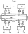
- FIG. 1 shows a data switching system with a plurality of switching units SUO to SUn. These switching units perform the switching functions required for the transmission of data signals based on the load sharing principle.
- the switching units are jointly connected to a ring line system.
- a ring line system can consist of a single closed ring line arrangement.
- Such a ring line system can, however, as shown in FIG. 1, for example, be made up of two parallel, independent ring line arrangements RING0 and RING1.
- Such redundancy makes it possible, for example, if one of the ring line arrangements fails, to carry out the transmission of signal blocks and acknowledgment signals on the other ring line arrangement.
- connection of the mentioned switching units SU0 to SUn The two ring line arrangements are each carried out via an interface circuit RA which is separate for each of the ring line arrangements and which will be discussed in more detail below.
- a plurality of line connection units TU0 to TUk are in each case connected to the ring line arrangements RING0 and RING1 again via an interface circuit RA separate for each of the ring line arrangements.
- These line connection units together with the associated interface circuits, serve for the data signal transmission between the aforementioned switching units and transmission lines connected to subscriber devices, which are connected to the line connection units TU0 to TUk.
- Each of the line connection units has a plurality of line connections LT0 to Ltm for such a connection of transmission lines.
- the circuit units formed from the aforementioned switching units or the line connection units and the associated interface circuits are also referred to below as control devices.
- control devices In the event that the ring line system consists of only one ring line arrangement, only one interface circuit belongs to a control device.
- data signals are transmitted in the form of signal blocks, each of which as data signals in the course of establishing a connection, signaling information and, in the case of an established connection, that between the subscriber devices in question have transmitting message signals.
- Each signal block to be transmitted contains in addition to the actual data signals, each consisting of a plurality of bits, e.g. B. 8 bits, are formed, at least one of the control devices as a receiver address, a start identifier denoting the start of a signal block, an end identifier denoting the end of a signal block, a sender address denoting the control unit emitting the signal block and at least one acknowledgment signal or an empty receipt.
- a signal block constructed in this way can only be delivered to one of the ring line arrangements if the control device in question has previously received a transmission authorization signal transmitted from control device to control device and controlling it in a transmission authorization state.
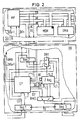
- FIG. 2 shows the structure of a control device in greater detail.
- a control device consists either of a switching unit or of a line connection unit, indicated in FIG. 2 by the designation SU / TU, and a number of interface circuits RA corresponding to the number of ring line arrangements. Only one of these interface circuits is shown in FIG. 2, since all of the interface circuits connected to the switching units or line connection units have the same internal structure.
- the unit shown in FIG. 2 with SU / TU and shown in sections has a microprocessor arrangement which controls both transmission and reception processes.
- Microprocessor MP a read-only memory (program memory) and read / write memory comprising memory arrangement MEM and a device for direct memory access DMA.
- the memory arrangement and the latter device are connected to the microprocessor MP via a bus line system.
- the bus line system consists of a data bus DB, an address bus AB and a control bus SB.
- the interface circuit RA is also connected to the microprocessor MP via the data bus and the lines of the control bus labeled RD and BC.
- INTn-1 and INTn lead to interrupt inputs IN-Tn-1 and INTn of the microprocessor MP.
- the interface circuit RA is connected to the device for direct memory access DMA via a further line labeled DMA.
- An interface circuit RA has both devices for the treatment of received signal blocks and acknowledgment signals and devices for the transmission of signal blocks available in the associated control device. In FIG. 2, of these devices, only the devices relating to the treatment of received signal blocks and acknowledgment signals relating to the present invention are shown.
- the interface circuit RA shown in FIG. 2 has a receive register Reg1 at the interface to the associated ring line arrangement, which may be the ring line arrangement RING0, for example, which receives signals transmitted in parallel via the ring line arrangement.
- This register is controlled by a clock generator, which Feeds clock signals corresponding to the transmission speed of the ring line arrangement to a clock input of the input register Reg1 via a line T.
- This input register is connected on the output side via a line arrangement ED on the one hand to a receive buffer arrangement EP and on the other hand to first inputs of a data switch DW1.
- the receive buffer arrangement serves, as will be explained in the following, for receiving signal blocks and acknowledgment signals and for forwarding them to the control device downstream in the ring line system.
- the receive buffer arrangement EP is connected to the unit SU / TU via the data bus DB, the lines RD and BC of the control bus SB already mentioned and via the lines DMA and INTn-1.
- the receive buffer arrangement receives clock signals via the already mentioned line T and itself outputs control signals via lines QE, QD, QK and F to a status register ZReg and via a line TL to a clock input of a register Reg2 serving as an acknowledgment receiver.
- the receive buffer arrangement is connected via a line arrangement ED 'to first inputs of a further data switch DW2.
- Second inputs of the data switch DW2 and data switch DW1 just mentioned are connected to outputs of the status register ZReg. Both data switches are controlled by the status register via lines SL1 and SL2.
- the data switch DW1 is connected to signal inputs of the already mentioned register Reg2, which is connected with its signal outputs to the data bus DB.
- the data switch DW2, on the other hand, is connected on the output side to signal inputs of an output register Reg3.
- This register receives Via the line T clock signals are supplied and at its signal outputs from the data switch DW2 signals supplied to the ring line arrangement connected to the interface circuit RA.
- the signal inputs of the output register are, moreover, also connected to devices for sending signal blocks available in the associated control device. However, as already mentioned, the structure of these facilities is not discussed in detail.
- data signals can optionally be transmitted to a single control device selected as a receiver or to a group of control devices. It is initially assumed that data signals from a control device of the ring line system are only to be transmitted to a single control device. For this transmission, the control device, from which the data signals are to be delivered, assembles the data signals in the associated unit SU / TU into a signal block. Such a signal block is shown schematically in FIG. 5a. It is initiated by a recipient address EADR which designates the control device selected as the recipient. The data signals DS1 to DSn to be transmitted follow this receiver address. Attached to these data signals is a transmitter address SADR that designates the control unit sending this signal block as a transmitter.
- SADR transmitter address
- a first identification bit designated A in FIG. 5, serves to identify the start of a signal block.
- the identification bit labeled E serves to identify the end of a signal block.
- the start and end of a signal block may be indicated, for example, by the logic state "1" of the respective identification bit.
- the logical state "1" of the identification bit A is referred to below as the block start identifier and the logical state "1" of the identification bit E as the block end identifier.
- the block start identifier is transmitted together with the recipient address and the block end identifier together with the sender address.
- a signal block compiled in the manner just described is then output upon arrival of a transmission authorization signal transmitted from the control device to the control device and controlling it in a transmission authorization state from the unit SU / TU (FIG. 2) via the output register Reg3 to the ring line arrangement connected to the interface circuit RA .
- Each of the interface circuits connected to the ring line arrangement receives the signals belonging to the transmitted signal block via the input register Reg1.
- a comparison is made of the receiver address transmitted in the signal block together with the block start identifier with the address assigned to the respective control device within the ring line system.
- the respective receive buffer arrangement EP continues to receive the received signal block unchanged via the line arrangement ED 'to the data switch DW2.
- the signal block then arrives at the ring line arrangement again via this and the output register Reg3.
- the signal block just received is copied in the receive buffer arrangement EP.
- the signal block itself is forwarded to the control device following in the ring line system by deleting the block start identifier (A) via the line arrangement ED '.
- the status register ZReg adds an acknowledgment signal (EADR, QS) to the transmitter address (SADR), so that the empty acknowledgment (LQ) originally contained in the signal block is overwritten.
- the status register ZReg receives a control signal from the receive buffer arrangement EP, which monitors the occurrence of the end-of-block identifier (E) and the sender address (SADR), via the line QE.
- the transmitted signal block is shown in FIG 5b.
- the reception buffer arrangement EP After the copying of a signal block mentioned, the reception buffer arrangement EP outputs a control signal indicating the availability of a received signal block via the line DMA to the device for direct memory access DMA. This device then causes the relevant signal block to be transferred to the SU / TU unit. The end of the signal block is indicated to the microprocessor MP by an interrupt signal at its interrupt input INTn-1 from the receive buffer arrangement EP.
- the block start identifier (A) originally transmitted in the signal block is deleted when it is forwarded, the signal block is no longer recognized as such, so that it cannot be picked up by subsequent control devices. Only the sender address (SADR) transmitted together with the block end identifier (E) can still be recognized as such.
- SADR sender address
- the occurrence of the end-of-block identifier and the sender address is monitored in the control device from which the signal block just acknowledged was previously delivered, specifically in the associated receive buffer arrangement EP. If the occurrence of end-of-block identification and sender address is recognized by the latter, it outputs a control signal via line TL to the associated acknowledgment register Reg2, which then receives the acknowledgment signal QS transmitted after the sender address from line arrangement ED via data switch DW1. Upon receipt of such an acknowledgment signal, the acknowledgment register issues an interrupt signal to the microprocessor MP via the line INTn. On the basis of this signal, the latter then accepts the acknowledgment signal available in the acknowledgment register for evaluation. A send process is now
- a signal block is to be transmitted to a group of control devices.
- a signal block is first compiled in the control device emitting the signal block in the manner shown in FIG. 5a and delivered to the ring line arrangement.
- the recipient address now designates a group of control devices.
- a group can optionally include all of the control devices belonging to the ring line arrangement or only a part of these control devices.
- the microprocessor MP of the control device in question also sends a broadcast signal BC to the receive buffer arrangement EP via the line of the same name.
- This broadcast signal indicates that a signal block has been delivered to a group of control devices.
- the signal block is again transmitted in the manner shown from control device to control device.
- Control devices that are not designated by the recipient address pass on the received signal block unchanged.
- the first control device belonging to the group designated by the recipient address copies the received signal block in the associated receive buffer arrangement EP.
- the signal block itself is passed on to the control device following in the ring line arrangement, omitting the previous block end identifier (E).
- the status register ZReg adds an acknowledgment information together with a block end identifier to the transmitter address (SADR) in response to a control signal emitted by the receive buffer arrangement, which is transmitted via the line QK.
- SADR transmitter address
- the acknowledgment information consists of the address (EADR1) assigned to the relevant control device within the ring line arrangement and the actual acknowledgment signal (QS1) relating to the reception of the signal block.
- the signal block emitted by the first control device belonging to the group is shown in FIG. 5c.
- the data switch DW2 shown in FIG. 2 is controlled accordingly via the line SL1 from the status register ZReg.
- the received signal block is copied to control devices and passed on to the control device following in the loop system, omitting the previous block end identifier. Acknowledgment information and a block end identifier are added to the last acknowledgment information transmitted in the signal block.
- the signal block emitted by the m-th control unit belonging to the group is shown in FIG. 5d. It follows from this that the signal block which the last control device belonging to the group emits has acknowledgment information for all control devices belonging to the group.
- the signal block containing the acknowledgment signals of all control devices belonging to the group is adopted in the control device from which the original signal block was emitted.
- This transfer can in turn take place in the form of a copying process in the associated receive buffer arrangement EP, to which a broadcast signal BC was supplied when the signal block was originally delivered.
- the copying process is initiated upon the occurrence of the block start identifier together with the broadcast signal.
- the signal block itself is returned to the associated ring line arrangement by deleting both the block start identifier and the block end identifier via the output register Reg3. Since both identifiers have now been deleted, the transmitted signal block can no longer be recognized by the control devices following in the ring line arrangement.
- the Receive buffer arrangement EP After copying the signal block including the acknowledgment information, ie when the end of block identification associated with this signal block occurs, the Receive buffer arrangement EP via the line QD from a control signal to the associated status register ZReg.
- This status register then provides an acknowledgment signal relating to the reception of this signal block, which is transferred to the acknowledgment register Reg2 via the data switch DW1.
- the acknowledgment register receives a corresponding control signal from the receive buffer arrangement via line TL.
- the data switch DW1 is controlled accordingly for this transfer from the status register ZReg via the line SL2.
- the receive buffer arrangement contains a read / write memory RAM with a plurality of memory cells for receiving signal blocks, including the associated block end identifiers.
- This memory is connected with its data signal inputs / outputs on the one hand for the reception of signal blocks with the line arrangement ED already shown in FIG. 2 and on the other hand for the delivery of signal blocks via a register Reg4 to the data bus DB also provided in FIG. He receives for the delivery of a signal block Reading clocks supplied via the line RD belonging to the control bus SB. These reading cycles correspond to the working speed of the respective control device.
- the read / write memory RAM is supplied with write clocks at an input WR. These write clocks occur on line T and are output via an AND gate G1 to the aforementioned input of the memory.
- This AND gate is controlled into the transferable state by a control signal appearing on a line ANF. This control signal is emitted by a receiving control EPS.
- the read / write memory is connected with its address inputs via a data switch DW3 on the one hand to a counter LZ and on the other hand to a counter SZ.
- the counter SZ serving as a write counter is connected with its clock input to the output of the previously mentioned AND gate G1, ie it receives the write clocks simultaneously with the read / write memory RAM.
- the counter SZ outputs its counter readings, which change in accordance with these write cycles, as address signals for the read / write memory.
- These counter outputs are also connected to a register Reg5, which receives a takeover clock via an AND gate G2.
- This AND gate is connected on the input side to line T and a line AK connected to the reception controller EPS.
- register Reg5 is connected to set inputs of counter SZ. These set inputs are released by a set signal appearing on a line F and output by the reception controller EPS.
- the counter LZ serves as a read counter. It receives the reading cycles occurring on line RD at its clock input and outputs its counter readings, which change according to these reading cycles, as address signals when reading a signal block to the read / write memory RAM.
- the data switch DW3 connected to the two counters mentioned is also connected to the line ANF with its control input.
- the receive buffer arrangement EP has a further counter IZ.
- This counter is an up / down counter which receives write clocks for counting in the one direction from the output of the AND gate G1 and for reading in the other direction the read clocks occurring on line RD.
- the counter IZ is connected to inputs of a decoder DEC, which at a specific counter reading of the counter IZ emits a message signal to the reception controller EPS via a line SUE.
- the counter IZ is also connected to a register Reg6 and to an OR gate G3.
- the register Reg6 receives a takeover clock at a clock input from the AND gate G2.
- this register is connected to set inputs of the counter IZ, which are released again by a set signal occurring on line F.
- OR gate G3 The output of the aforementioned OR gate G3 is connected to first inputs of an OR gate G4.
- This OR gate is connected to the negating output of a flip-flop FF with a further input.
- the output of the OR gate G4 is on line DMA connected.
- the non-negating output of flip-flop FF on the other hand, is connected to line INTn-1.
- the clock input of this flip-flop receives the reading clocks occurring on line RD.
- the data input of the flip-flop is connected to the line EK of the data bus DB which carries the block end identifier.
- the already mentioned receive control EPS is connected to a plurality of the lines shown in FIG. 2.
- these are the line arrangement ED and the lines BC and T.
- On the output side there is a connection on the one hand to the line arrangement ED 'and on the other hand to the lines TL, QE, QD, QK and F.
- the reception controller EPS emits a control signal via the line ANF.
- write / read memory RAM and the two counters SZ and IZ are supplied with write pulses for the reception of a received signal block via AND gate G1.
- Both counters may initially be in a basic counter reading, which may be counter reading "0", for example.
- the counter status is then changed with each write cycle, the memory cells of the read / write memory RAM being continuously addressed with the changing current counter status of the counter SZ, while the current counter status of the counter IZ corresponds to the current fill level of the read / write memory corresponds.
- the presence of a received signal block from the unit SU / TU is indicated by a control signal transmitted via the line DMA.
- the signal block located in the read / write memory is then converted into the unit by supplying read clocks via the line RD and continuously addressing the memory cells of the read / write memory from the counter LZ by means of direct memory access via the register Reg4 SU / TU taken over until the block end identifier contained in the signal block just read occurs.
- This end of block identifier occurs on line EK1 of data bus DB.
- This occurrence brings the flip-flop FF into its active state, in which it signals the microprocessor the end of a signal block via the line INTn-1.
- the microprocessor then interrupts the supply of further reading cycles.
- the flip-flop FF interrupts the control signal transmitted via line DMA for direct memory access.
- the counter LZ may also begin to count from a predetermined basic counter reading, which may also be the counter reading "0". The instantaneous counter reading which is then given by the counter LZ when the end of the block occurs occurs until a further reading process is initiated.
- the read clocks are also fed to the counter IZ. These reading cycles cause counting in the reverse direction, so that the current counter reading of this counter is reduced with each reading cycle.
- the current counter reading thus corresponds to the number of signals in the signal block which have not yet been read from the read / write memory.
- the OR gate G4 is blocked so that the supply of the control signal transmitted via the line DMA is interrupted.
- the control processes already explained also run again.
- the counters SZ, LZ and IZ continue to count from their pending counter readings.
- the initial counter readings of these counters now correspond to the counter readings last reached when transferring or reading out signal blocks.
- the rewriting of signal blocks in the read / write memory can also take place at a point in time at which previously received signal blocks have not yet or not yet been completely adopted into the unit SU / TU. In this case, the recording of a signal block just received has priority over the reading of previously received signal blocks.
- the counter IZ changes its counter reading in accordance with the number of memory cells in the read / write memory RAM which are occupied by signals from the signal blocks and have not yet been read out.
- a signal transmitted via line AK is used to indicate the occurrence of the block start identifier transmitted with it issued a takeover clock via the AND gate G2 to the two registers REG5 and Reg6. Each of these then takes over the current counter reading given by its associated counter as the initial counter reading for a further recording of signal blocks.
- the decoder does so DEC forth a message signal to the receiving controller EPS, which then transmits via the line F a set signal for the release of the set inputs of the counters SZ and IZ.
- the initial counter readings transferred to registers Reg5 and Reg6 at the beginning of the signal block just received are thus transferred to counters SZ and IZ, i.e. the memory cells of the write / store RAM, which have already been occupied by signals from the signal block which cannot be completely recorded, are released again.
- the recording of the signal block just received in the read / write memory is ended. This is done by blocking the AND gate G1 on the basis of a control signal transmitted via the line ANF.
- the incomplete recording of a signal block is also signaled via line F to the status register ZReg shown in FIG. 2, which then appends a corresponding acknowledgment signal to the transmitter address transmitted with the signal block just received.
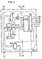
- FIG. 4 shows the structure of the reception control EPS.
- This contains two comparator arrangements Vg11 and Vg12 for comparing the receiver address transmitted in a signal block together with the block start identifier or that together with an acknowledgment signal Transmitted sender address with an address assigned to the associated control device within the ring line arrangement.
- the comparator arrangement Vg11 is used for an address comparison when a signal block intended only for one of the control devices is received and when an acknowledgment signal is received.
- the comparator arrangement VGL2, on the other hand is used for address comparison when a signal block intended for a group of control devices is received.
- the comparison address to be used for the respective comparison is provided by an arrangement S1 or S2, which is connected to the comparator arrangement Vg11 or Vg12 and is represented as a switch arrangement. These arrangements can be any storage devices.
- the comparator arrangement to be used for an address comparison is controlled by a signal on line GA. This signal is part of the receiver address that designates a group of control devices and designates it as such.
- the outputs of the two comparator arrangements are connected via an OR gate G5 to one of the address inputs of a read-only memory PROM. Further address inputs of this memory are connected to a line AK carrying the block start identifier, a line EK2 carrying the block end identifier, the lines SUE, BC and to the output of the comparator arrangement Vg12.
- the two lines AK and EK2 are associated with the line arrangement ED.
- the read-only memory PROM has a plurality of memory locations in which all control signals for the treatment of received signal blocks and acknowledgment signals are stored.
- This read-only memory is connected to a register Reg7 with its data outputs.
- This register is connected via data outputs to the lines ANF, QE, QD, QK, TL and F already shown in FIG.
- a data output is also connected to a first control input of a Reg8 register.
- the register is Reg7 with a clock input finally connected to line T.
- a second control input of the register Reg8 is connected to the line BC already shown in FIG. This register is connected on the input side to the line arrangement ED and on the output side to the line arrangement ED '.
- the read-only memory PROM Depending on the signals that the read-only memory PROM is currently receiving at its address inputs, it emits a control signal corresponding to these signals, which is accepted by the register Reg7 and sent to the line in question.
- the effect of the control signals occurring on the lines ANF, QE, QD, QK, TL and F has already been explained with reference to FIG. 2.
- Each of the signal blocks received by the associated control device is forwarded via register Reg8 to the control device downstream in the ring line arrangement.
- the signal block in question is possibly treated with regard to the block start identifier and block end identifier contained in it.
- the treatment consists, as already mentioned above, in that, depending on the type of signal block to be forwarded, the block start identifier, the block end identifier or both identifiers are deleted.
Abstract
Description
Die Erfindung betrifft ein Verfahren und eine Schaltungsanordnung zum Übertragen von Datensignalen zwischen über ein taktgesteuertes, richtungsabhängig betriebenes Ringleitungssystem miteinander verbundenen Steuereinrichtungen, nach dem Obergriff des Anspruchs 1 bzw. des Anspruchs 2.The invention relates to a method and a circuit arrangement for transmitting data signals between control devices connected to one another via a clock-controlled, directionally dependent ring line system, according to the preamble of
Ein Verfahren der gerade genannten Art ist aus dem Artikel in PROCEEDINGS OF THE SIXTH INTERNATIONAL CONFERENCE ON COMPUTER COMMUNICATION, London, GB, 7.-10. September 1982, Seiten 496-501, North-Holland Publishing Co., Amsterdam, NL; K.YAGYU et al.: "High throughput optical fiber loop network with effective detection mechanism of lost or duplicated token" bekannt.A method of the type just mentioned is from the article in PROCEEDINGS OF THE SIXTH INTERNATIONAL CONFERENCE ON COMPUTER COMMUNICATION, London, GB, 7-10. September 1982, pages 496-501, North-Holland Publishing Co., Amsterdam, NL; K.YAGYU et al .: "High throughput optical fiber loop network with effective detection mechanism of lost or duplicated token".
Es ist nun Aufgabe der vorliegenden Erfindung, einen Weg zu zeigen, wie bei einem Verfahren und einer Schaltungsanordnung der eingangs genannten Art Signalblöcke und Quittungssignale zwischen zwei zu dem Ringleitungssystem gehörenden Steuereinrichtungen sicher und mit einem geringen Steuerungsaufwand übertragen werden können, insbesondere wenn über das Ringleitungssystem Signalblöcke mit variabler Länge übertragen werden.It is an object of the present invention to show a way in which, in a method and a circuit arrangement of the type mentioned at the outset, signal blocks and acknowledgment signals can be transmitted safely and with little control effort between two control devices belonging to the ring line system, in particular if signal blocks are transmitted via the ring line system can be transmitted with variable length.
Gelöst wird die vorstehend aufgezeigte Aufgabe bei einem Verfahren der eingangs genannten Art erfindungsgemäß durch die Merkmale des kennzeichnenden Teils des Anspruchs 1 und bei einer Anordung der eingangs genannten Art durch die Merkmale des kennzeichnenden Teils des Anspruchs 2.The above-mentioned object is achieved according to the invention in a method of the type mentioned at the outset by the features of the characterizing part of
Das Verfahren nach dem Anspruch 1 bringt den Vorteil mit sich, daß für die Erzeugung eines für den Sender eines gerade empfangenen Signalblockes bestimmten Quittungssignals der empfangene Signalblock unmittelbar herangezogen wird, indem unter Löschung der zu dem Signalblock gehörenden Blockanfangskennung lediglich an die durch die Blockendekennung gekennzeichnete Senderadresse ein den Empfang des Signalblockes betreffendes Quittungssignal angefügt wird. Durch die Löschung der Blockanfangskennung ist der weitergeleitete Signalblock nicht mehr als solcher gekennzeichnet. Erkennbar ist jedoch noch die in Verbindung mit der Blockendekennung übertragene Senderadresse, an die von der als Empfänger ausgewählten Steuereinrichtung ein den Empfang des Signalblockes betreffendes Quittungssignal angefügt ist. In derjenigen Steuereinrichtung, von der zuvor der Signalblock abgegeben worden ist, braucht somit lediglich das Auftreten der Senderadresse in Verbindung mit der Blockendekennung überwacht zu werden, um das für sie bestimmte Quittungssignal zu übernehmen.The method according to
Die Schaltungsanordnung nach dem Anspruch 2 weist eine Empfangssteuerung und eine aus einem Empfangsspeicher für die Aufnahme von Signalblöcken und einem Quittungsempfänger bestehende Empfängeranordnung auf. Durch die Trennung der Empfängeranordnung in einen Empfangsspeicher und in einen Quittungsempfänger ist es möglich, mit einem geringen Steuerungsaufwand Signalblöcke und Quittungssignale in die jeweilige Steuereinrichtung aufzunehmen und diese in der jeweiligen Empfängeranordnung nachgeschalteten Einrichtungen zu verarbeiten.The circuit arrangement according to
Vorteilhafte Ausgestaltungen der Schaltungsanordnung gemäß Patentanspruch 2 gehen aus den Patentansprüchen 3 bis 8 hervor. Ein Vorteil der den Empfangsspeicher betreffenden Ausgestaltungen besteht u. a.darin, daß durch das Vorhandensein eines für den Ablauf von Schreib- und Lesevorgängen von zwei gesonderten Anordnungen her steuerbaren Schreib-/Lese-Speichers eine Anpassung der Arbeitsgeschwindigkeit der Steuereinrichtungen an die Übertragungsgeschwindigkeit innerhalb des Ringleitungssystems möglich ist. Dabei ist es im Hinblick auf den Steuerungsaufwand zweckmäßig, wenn der Schreib-/Lese-Speicher durch die Zähleranordnungen entsprechend dem Patentanspruch 4 umlaufend adressiert wird. Um bei dieser umlaufenden Adressierung des Schreib-/Lese-Speichers ein Überschreiben von bereits in dem Schreib-/Lese-Speicher gespeicherten, jedoch noch nicht ausgelesenen Signalblöcklen zu vermeiden, ist es vorteilhaft, eine Zähleranordnung gemäß Patentanspruch 5 vorzusehen, die den Füllstand des Schreib-/Lese-Speichers überwacht und bei Erreichen eines vorgegebenen Füllstandes die Aufnahme des gerade empfangenen Signalblockes durch eine entsprechende Beeinflussung der für die Abwicklung von Schreibvorgängen vorgesehenen Zähleranordnung abbricht. Eine lediglich einen geringen schaltungstechnischen Aufwand erfordernde Anordnung für die Steuerung der beiden zuletzt genannten Zähleranordnungen bei Abbruch der Aufnahme eines gerade empfangenen Signalblockes geht aus Patentanspruch 6 hervor.Advantageous refinements of the circuit arrangement according to
Die Patentansprüche 7 und 8 beziehen sich auf vorteilhafte Ausgestaltungen der Empfangssteuerung und des Quittungsempfängers. Die Empfangssteuerung und der Quittungsempfänger zeichnen sich dabei sowohl durch einen geringen schaltungstechnischen Aufwand als auch durch einen geringen Steuerungsaufwand aus.
Im folgenden wird die Erfindung anhand von Zeichnungen beispielsweise näher erläutert.
- FIG 1
- zeigt in einem Blockschaltbild ein aus einem Ringleitungssystem gebildetes Datenvermittlungssystem, bei dem die Erfindung angewandt ist,
- FIG 2
- zeigt in einem Blockschaltbild ausschnittweise den Aufbau einer der in FIG 1 lediglich schematisch dargestellten Schnittstellenschaltungen und den Aufbau einer mit dieser verbundenen Vermittlungseinheit bzw. Leitungsanschlußeinheit,
- FIG 3
- zeigt den Aufbau einer in der Schnittstellenschaltung gemäß FIG 2 vorhandenen Empfangspuffer-Anordnung,
- FIG 4
- zeigt den Aufbau einer der Empfangspuffer-Anordnung gemäß FIG 3 zugehörigen Empfangssteuerung und
- FIG 5
- gibt die Struktur von Signalblöcken wieder, welche über das Ringleitungssystem übertragen werden.
- FIG. 1
- 1 shows a block circuit diagram of a data switching system formed from a ring line system, in which the invention is applied,
- FIG 2
- 1 shows in a block diagram a section of the structure of one of the interface circuits shown only schematically in FIG. 1 and the structure of a switching unit or line connection unit connected to it,
- FIG 3
- 2 shows the structure of a receive buffer arrangement in the interface circuit according to FIG. 2,
- FIG 4
- shows the structure of a receive control associated with the receive buffer arrangement according to FIG 3 and
- FIG 5
- reproduces the structure of signal blocks that are transmitted via the loop system.
In FIG 1 ist ein Datenvermittlungssystem mit einer Mehrzahl von Vermittlungseinheiten SUO bis SUn dargestellt. Diese Vermittlungseinheiten führen nach dem Lastteilungsprinzip die für die Übertragung von Datensignalen erforderlichen Vermittlungsfunktionen aus. Die Vermittlungseinheiten sind dafür gemeinsam an ein Ringleitungssystem angeschlossen. Ein solches Ringleitungssystem kann aus einer einzigen geschlossen Ringleitungsanordnung bestehen. Ein solches Ringleitungssystem kann jedoch auch, wie in FIG 1 beispielsweise dargestellt, aus zwei parallel verlaufenden, voneinander unabhängigen Ringleitungsanordnungen RING0 und RING1 aufgebaut sein. Durch eine solche Redundanz ist es beispielsweise bei Ausfall einer der Ringleitungsanordnungen möglich, die Übertragung von Signalblöcken und Quittungssignalen auf der jeweils anderen Ringleitungsanordnung auszuführen.1 shows a data switching system with a plurality of switching units SUO to SUn. These switching units perform the switching functions required for the transmission of data signals based on the load sharing principle. For this purpose, the switching units are jointly connected to a ring line system. Such a ring line system can consist of a single closed ring line arrangement. Such a ring line system can, however, as shown in FIG. 1, for example, be made up of two parallel, independent ring line arrangements RING0 and RING1. Such redundancy makes it possible, for example, if one of the ring line arrangements fails, to carry out the transmission of signal blocks and acknowledgment signals on the other ring line arrangement.
Der Anschluß der genannten Vermittlungseinheiten SU0 bis SUn an die beiden Ringleitungsanordnungen erfolgt jeweils über eine für jede der Ringleitungsanordnungen gesonderte Schnittstellenschaltung RA, auf die im folgenden noch näher eingegangen wird.The connection of the mentioned switching units SU0 to SUn The two ring line arrangements are each carried out via an interface circuit RA which is separate for each of the ring line arrangements and which will be discussed in more detail below.
Mit den genannten Ringleitungsanordnungen RING0 und RING1 ist außerdem eine Mehrzahl von Leitungsanschlußeinheiten TU0 bis TUk jeweils wieder über eine für jede der Ringleitungsanordnungen gesonderte Schnittstellenschaltung RA verbunden. Diese Leitungsanschlußeinheiten dienen zusammen mit den zugehörigen Schnittstellenschaltungen für die Datensignalübertragung zwischen den genannten Vermittlungseinheiten und mit Teilnehmereinrichtungen verbundenen Übertragungsleitungen, die an die Leitungsanschlußeinheiten TU0 bis TUk angeschlossen sind. Jede der Leitungsanschlußeinheiten weist für einen solchen Anschluß von Übertragungsleitungen eine Mehrzahl von Leitungsanschlüssen LT0 bis Ltm auf.A plurality of line connection units TU0 to TUk are in each case connected to the ring line arrangements RING0 and RING1 again via an interface circuit RA separate for each of the ring line arrangements. These line connection units, together with the associated interface circuits, serve for the data signal transmission between the aforementioned switching units and transmission lines connected to subscriber devices, which are connected to the line connection units TU0 to TUk. Each of the line connection units has a plurality of line connections LT0 to Ltm for such a connection of transmission lines.
Die aus den genannten Vermittlungseinheiten bzw. den Leitungsanschlußeinheiten und den zugehörigen Schnittstellenschaltungen gebildeten Schaltungseinheiten werden im folgenden auch als Steuereinrichtungen bezeichnet. Für den Fall, daß das Ringleitungssystem lediglich aus einer einzigen Ringleitungsanordnung besteht, gehört zu einer Steuereinrichtung lediglich eine einzige Schnittstellenschaltung.The circuit units formed from the aforementioned switching units or the line connection units and the associated interface circuits are also referred to below as control devices. In the event that the ring line system consists of only one ring line arrangement, only one interface circuit belongs to a control device.
Innerhalb des in FIG 1 dargestellten Vermittlungssystems, d. h. zwischen den Vermittlungseinheiten und den Leitungsanschlußeinheiten erfolgt die Übertragung von Datensignalen in Form von Signalblöcken, welche jeweils als Datensignale im Zuge des Aufbaus einer Verbindung Signalisierungsinformationen und bei einer eingerichteten Verbindung die zwischen den in Frage kommenden Teilnehmereinrichtungen zu übertragenden Nachrichtensignale aufweisen. Dabei enthält jeder zu übertragende Signalblock neben den eigentlichen Datensignalen, die jeweils aus einer Mehrzahl von Bits, z. B. 8 Bits, gebildet sind, eine mindestens eine der Steuereinrichtungen als Empfänger bezeichnende Empfängeradresse, eine den Beginn eines Signalblockes bezeichnende Anfangskennung, eine das Ende eines Signalblockes bezeichnende Endekennung, eine die den Signalblock abgebende Steuereinrichtung als Sender bezeichnende Senderadresse und mindestens ein Quittungssignal bzw. eine Leerquittung. Ein derartig aufgebauter Signalblock, auf den im folgenden noch näher eingegangen wird, kann dabei nur dann an eine der Ringleitungsanordnungen abgegeben werden, wenn zuvor von der in Frage kommenden Steuereinrichtung ein von Steuereinrichtung zu Steuereinrichtung übertragenes, diese jeweils in einen Sendeberechtigungszustand steuerndes Sendeberechtigungssignal empfangen wurde.Within the switching system shown in FIG 1, ie between the switching units and the line connection units, data signals are transmitted in the form of signal blocks, each of which as data signals in the course of establishing a connection, signaling information and, in the case of an established connection, that between the subscriber devices in question have transmitting message signals. Each signal block to be transmitted contains in addition to the actual data signals, each consisting of a plurality of bits, e.g. B. 8 bits, are formed, at least one of the control devices as a receiver address, a start identifier denoting the start of a signal block, an end identifier denoting the end of a signal block, a sender address denoting the control unit emitting the signal block and at least one acknowledgment signal or an empty receipt. A signal block constructed in this way, which will be dealt with in more detail below, can only be delivered to one of the ring line arrangements if the control device in question has previously received a transmission authorization signal transmitted from control device to control device and controlling it in a transmission authorization state.
In FIG 2 ist der Aufbau einer Steuereinrichtung detaillierter dargestellt. Wie bereits oben erwähnt, besteht eine solche Steuereinrichtung entweder aus einer Vermittlungseinheit oder aus einer Leitungsanschlußeinheit, in FIG 2 durch die Bezeichnung SU/TU angedeutet, und einer der Anzahl der Ringleitungsanordnungen entsprechenden Anzahl von Schnittstellenschaltungen RA. Dabei ist in FIG 2 lediglich eine dieser Schnittstellenschaltungen gezeigt, da sämtliche mit den Vermittlungseinheiten bzw. Leitungsanschlußeinheiten verbundenen Schnittstellenschaltungen intern den gleichen Aufbau aufweisen.2 shows the structure of a control device in greater detail. As already mentioned above, such a control device consists either of a switching unit or of a line connection unit, indicated in FIG. 2 by the designation SU / TU, and a number of interface circuits RA corresponding to the number of ring line arrangements. Only one of these interface circuits is shown in FIG. 2, since all of the interface circuits connected to the switching units or line connection units have the same internal structure.
Die in FIG 2 mit SU/TU bezeichnete, ausschnittweise dargestellte Einheit (Vermittlungseinheit oder Leitungsanschlußeinheit) weist eine sowohl Sende- als auch Empfangsvorgänge steuernde Mikroprozessoranordnung auf. Von dieser Mikroprozessoranordnung sind dargestellt ein Mikroprozessor MP, eine Festwertspeicher (Programmspeicher) und Schreib-/Lese-Speicher umfassende Speicheranordnung MEM und eine Einrichtung für einen direkten Speicherzugriff DMA. Die Speicheranordnung und die zuletzt genannte Einrichtung stehen dabei über ein Busleitungssystem mit dem Mikroprozessor MP in Verbindung. Das Busleitungssystem besteht aus einem Datenbus DB, einem Adressbus AB und einem Steuerbus SB. Über den Datenbus und über die mit RD und BC bezeichneten Leitungen des Steuerbusses steht auch die Schnittstellenschaltung RA mit dem Mikroprozessor MP in Verbindung. Weiterhin führen zwei mit INTn-1 und INTn bezeichnete Steuerleitungen der Schnittstellenschaltung zu Unterbrechungseingängen IN-Tn-1 und INTn des Mikroprozessors MP hin. Schließlich ist die Schnittstellenschaltung RA noch über eine weitere mit DMA bezeichnete Leitung mit der Einrichtung für einen direkten Speicherzugriff DMA verbunden.The unit shown in FIG. 2 with SU / TU and shown in sections (switching unit or line connection unit) has a microprocessor arrangement which controls both transmission and reception processes. Of this microprocessor arrangement are shown Microprocessor MP, a read-only memory (program memory) and read / write memory comprising memory arrangement MEM and a device for direct memory access DMA. The memory arrangement and the latter device are connected to the microprocessor MP via a bus line system. The bus line system consists of a data bus DB, an address bus AB and a control bus SB. The interface circuit RA is also connected to the microprocessor MP via the data bus and the lines of the control bus labeled RD and BC. Furthermore, two control lines of the interface circuit designated INTn-1 and INTn lead to interrupt inputs IN-Tn-1 and INTn of the microprocessor MP. Finally, the interface circuit RA is connected to the device for direct memory access DMA via a further line labeled DMA.
Eine Schnittstellenschaltung RA weist sowohl Einrichtungen für die Behandlung empfangener Signalblöcke und Quittungssignale als auch Einrichtungen für das Aussenden von in der zugehörigen Steuereinrichtung bereitstehenden Signalblöcken auf. In FIG 2 sind von diesen Einrichtungen lediglich die auf die vorliegende Erfindung sich beziehenden Einrichtungen für die Behandlung empfangener Signalblöcke und Quittungssignale dargestellt.An interface circuit RA has both devices for the treatment of received signal blocks and acknowledgment signals and devices for the transmission of signal blocks available in the associated control device. In FIG. 2, of these devices, only the devices relating to the treatment of received signal blocks and acknowledgment signals relating to the present invention are shown.
Die in FIG 2 dargestellte Schnittstellenschaltung RA weist an der Schnittstelle zu der zugehörigen Ringleitungsanordnung, die beispielsweise die Ringleitungsanordnung RING0 sein möge, ein Empfangsregister Reg1 auf, welches in paralleler Form über die Ringleitungsanordnung übertragene Signale zugeführt erhält. Gesteuert wird dieses Register dazu von einem Taktgenerator her, welcher über eine Leitung T der Übertragungsgeschwindigkeit der Ringleitungsanordnung entsprechende Taktsignale einem Takteingang des Eingangsregisters Reg1 zuführt. Dieses Eingangsregister ist ausgangsseitig über eine Leitungsanordnung ED einerseits mit einer Empfangspuffer-Anordnung EP und andererseits mit ersten Eingängen einer Datenweiche DW1 verbunden. Die Empfangspuffer-Anordnung dient dabei, wie im folgenden noch erläutert werden wird, für die Aufnahme von Signalblöcken und Quittungssignalen sowie für deren Weiterleitung an die im Ringleitungssystem nachfolgende Steuereinrichtung.The interface circuit RA shown in FIG. 2 has a receive register Reg1 at the interface to the associated ring line arrangement, which may be the ring line arrangement RING0, for example, which receives signals transmitted in parallel via the ring line arrangement. This register is controlled by a clock generator, which Feeds clock signals corresponding to the transmission speed of the ring line arrangement to a clock input of the input register Reg1 via a line T. This input register is connected on the output side via a line arrangement ED on the one hand to a receive buffer arrangement EP and on the other hand to first inputs of a data switch DW1. The receive buffer arrangement serves, as will be explained in the following, for receiving signal blocks and acknowledgment signals and for forwarding them to the control device downstream in the ring line system.
Die Empfangspuffer-Anordnung EP steht über den Datenbus DB, die bereits erwähnten Leitungen RD und BC des Steuerbusses SB und über die Leitungen DMA und INTn-1 mit der Einheit SU/TU in Verbindung. Die Empfangspuffer-Anordnung erhält über die bereits erwähnte Leitung T Taktsignale zugeführt und gibt selbst Steuersignale über Leitungen QE, QD, QK und F an ein Zustandsregister ZReg und über eine Leitung TL an einen Takteingang eines als Quittungsempfänger dienenden Registers Reg2 ab. Die Empfangspuffer-Anordnung steht schließlich noch über eine Leitungsanordnung ED' mit ersten Eingängen einer weiteren Datenweiche DW2 in Verbindung.The receive buffer arrangement EP is connected to the unit SU / TU via the data bus DB, the lines RD and BC of the control bus SB already mentioned and via the lines DMA and INTn-1. The receive buffer arrangement receives clock signals via the already mentioned line T and itself outputs control signals via lines QE, QD, QK and F to a status register ZReg and via a line TL to a clock input of a register Reg2 serving as an acknowledgment receiver. Finally, the receive buffer arrangement is connected via a line arrangement ED 'to first inputs of a further data switch DW2.
Zweite Eingänge der gerade erwähnten Datenweiche DW2 und der Datenweiche DW1 sind mit Ausgängen des Zustandsregisters ZReg verbunden. Beide Datenweichen werden dabei von dem Zustandsregister her über die Leitungen SL1 und SL2 gesteuert. Ausgangsseitig ist die Datenweiche DW1 an Signaleingänge des bereits erwähnten Registers Reg2 angeschlossen, welches mit seinen Signalausgängen mit dem Datenbus DB verbunden ist. Die Datenweiche DW2 ist dagegen ausgangsseitig an Signaleingänge eines Ausgangsregisters Reg3 angeschlossen. Dieses Register erhält über die Leitung T Taktsignale zugeführt und gibt an seinen Signalausgängen von der Datenweiche DW2 her zugeführte Signale an die mit der Schnittstellenschaltung RA verbundene Ringleitungsanordnung ab. Die Signaleingänge des Ausgangsregisters stehen im übrigen auch noch mit Einrichtungen für das Aussenden von in der zugehörigen Steuereinrichtung bereitstehenden Signalblöcken in Verbindung. Wie jedoch bereits erwähnt, wird auf den Aufbau dieser Einrichtungen nicht näher eingegangen.Second inputs of the data switch DW2 and data switch DW1 just mentioned are connected to outputs of the status register ZReg. Both data switches are controlled by the status register via lines SL1 and SL2. On the output side, the data switch DW1 is connected to signal inputs of the already mentioned register Reg2, which is connected with its signal outputs to the data bus DB. The data switch DW2, on the other hand, is connected on the output side to signal inputs of an output register Reg3. This register receives Via the line T clock signals are supplied and at its signal outputs from the data switch DW2 signals supplied to the ring line arrangement connected to the interface circuit RA. The signal inputs of the output register are, moreover, also connected to devices for sending signal blocks available in the associated control device. However, as already mentioned, the structure of these facilities is not discussed in detail.
Im folgenden wird nun zunächst das Zusammenwirken der in FIG 2 dargestellten Schaltungsteile bei der Aufnahme und Weiterleitung von Signalblöcken und Quittungssignalen erläutert, ehe auf den Aufbau der Empfangspuffer-Anordnung EP näher eingegangen wird.The interaction of the circuit parts shown in FIG. 2 during the recording and forwarding of signal blocks and acknowledgment signals will now be explained below, before the structure of the receive buffer arrangement EP is discussed in more detail.
Innerhalb des Ringleitungssystems können Datensignale wahlweise an eine einzige als Empfänger ausgewählte Steuereinrichtung oder an eine Gruppe von Steuereinrichtungen übertragen werden. Es wird dabei zunächst davon ausgegangen, daß Datensignale von einer Steuereinrichtung des Ringleitungssystems her lediglich an eine einzige Steuereinrichtung zu übertragen sind. Für diese Übertragung stellt die Steuereinrichtung, von der die Datensignale abzugeben sind, die Datensignale in der zugehörigen Einheit SU/TU zu einem Signalblock zusammen. Ein derartiger Signalblock ist in FIG 5a schematisch dargestellt. Er wird durch eine die als Empfänger ausgewählte Steuereinrichtung bezeichnende Empfängeradresse EADR eingeleitet. Dieser Empfängeradresse folgen die zu übertragenden Datensignale DS1 bis DSn. Angefügt ist diesen Datensignalen eine die diesen Signalblock sendende Steuereinrichtung als Sender bezeichnende Senderadresse SADR. Der Signalblock wird schließlich durch eine vom Sender vorbereitete Leerquittung LQ abgeschlossen. Den genannten Signalen eines Signalblockes sind jeweils u. a. zwei Kennbits beigefügt. Ein erstes, in FIG 5 mit A bezeichnetes Kennbit dient zur Kennzeichnung des Anfangs eines Signalblockes. In entsprechender Weise dient das mit E bezeichnete Kennbit zur Kennzeichnung des Endes eines Signalblockes. Der Anfang und das Ende eines Signalblockes mögen dabei beispielsweise durch den logischen Zustand "1" des jeweiligen Kennbits angezeigt werden. Der logische Zustand "1" des Kennbits A wird im folgenden als Blockanfangskennung und der logische Zustand "1" des Kennbits E als Blockendekennung bezeichnet. Wie in FIG 5a dargestellt, wird die Blockanfangskennung zusammen mit der Empfängeradresse und die Blockendekennung zusammen mit der Senderadresse übertragen.Within the ring line system, data signals can optionally be transmitted to a single control device selected as a receiver or to a group of control devices. It is initially assumed that data signals from a control device of the ring line system are only to be transmitted to a single control device. For this transmission, the control device, from which the data signals are to be delivered, assembles the data signals in the associated unit SU / TU into a signal block. Such a signal block is shown schematically in FIG. 5a. It is initiated by a recipient address EADR which designates the control device selected as the recipient. The data signals DS1 to DSn to be transmitted follow this receiver address. Attached to these data signals is a transmitter address SADR that designates the control unit sending this signal block as a transmitter. The signal block is finally replaced by a Empty acknowledgment LQ prepared by the sender completed. Two signals are added to each of the signals mentioned in a signal block. A first identification bit, designated A in FIG. 5, serves to identify the start of a signal block. In a corresponding manner, the identification bit labeled E serves to identify the end of a signal block. The start and end of a signal block may be indicated, for example, by the logic state "1" of the respective identification bit. The logical state "1" of the identification bit A is referred to below as the block start identifier and the logical state "1" of the identification bit E as the block end identifier. As shown in FIG. 5a, the block start identifier is transmitted together with the recipient address and the block end identifier together with the sender address.
Ein in der gerade beschriebenen Weise zusammengestellter Signalblock wird anschließend bei Eintreffen eines von Steuereinrichtung zu Steuereinrichtung übertragenen, diese jeweils in einen Sendeberechtigungszustand steuernden Sendeberechtigungssignals von der Einheit SU/TU (FIG 2) her über das Ausgangsregister Reg3 an die mit der Schnittstellenschaltung RA verbundene Ringleitungsanordnung abgegeben. Jede der mit der Ringleitungsanordnung verbundenen Schnittstellenschaltungen nimmt die zu dem übertragenen Signalblock gehörenden Signale über das Eingangsregister Reg1 auf. Dabei wird zunächst mit Hilfe der der jeweiligen Steuereinrichtung zugehörigen Empfangspuffer-Anordnung EP ein Vergleich der in dem Signalblock zusammen mit der Blockanfangskennung übertragenen Empfängeradresse mit der der jeweiligen Steuereinrichtung innerhalb des Ringleitungssystems zugewiesenen Adresse durchgeführt. Ergibt der Vergleich keine Übereinstimmung der miteinander verglichenen Adressen, so leitet die jeweilige Empfangspuffer-Anordnung EP den empfangenen Signalblock unverändert über die Leitungsanordnung ED' an die Datenweiche DW2 weiter. Über diese und das Ausgangsregister Reg3 gelangt dann der Signalblock wieder auf die Ringleitungsanordnung.A signal block compiled in the manner just described is then output upon arrival of a transmission authorization signal transmitted from the control device to the control device and controlling it in a transmission authorization state from the unit SU / TU (FIG. 2) via the output register Reg3 to the ring line arrangement connected to the interface circuit RA . Each of the interface circuits connected to the ring line arrangement receives the signals belonging to the transmitted signal block via the input register Reg1. First of all, with the aid of the receive buffer arrangement EP belonging to the respective control device, a comparison is made of the receiver address transmitted in the signal block together with the block start identifier with the address assigned to the respective control device within the ring line system. If the comparison does not reveal a match between the compared addresses, the respective receive buffer arrangement EP continues to receive the received signal block unchanged via the line arrangement ED 'to the data switch DW2. The signal block then arrives at the ring line arrangement again via this and the output register Reg3.
Ergibt dagegen der Adressenvergleich eine Übereinstimmung der miteinander verglichenen Adressen, so wird der gerade empfangene Signalblock in der Empfangspuffer-Anordnung EP kopiert. Der Signalblock selbst wird unter Löschung der Blockanfangskennung (A) über die Leitungsanordnung ED' an die im Ringleitungssystem folgende Steuereinrichtung weitergeleitet. Bei diesem Weiterleiten fügt das Zustandsregister ZReg an die Senderadresse (SADR) noch ein Quittungssignal (EADR, QS) an, so daß die ursprünglich in dem Signalblock enthaltene Leerquittung (LQ) überschrieben wird. Für dieses Anfügen erhält das Zustandsregister ZReg von der Empfangspuffer-Anordnung EP, die das Auftreten der Blockendekennung (E) und der Senderadresse (SADR) überwacht, ein Steuersignal über die Leitung QE zugeführt. Der weitergeleitete Signalblock ist in FIG 5b dargestellt.If, on the other hand, the address comparison shows that the addresses compared with one another match, the signal block just received is copied in the receive buffer arrangement EP. The signal block itself is forwarded to the control device following in the ring line system by deleting the block start identifier (A) via the line arrangement ED '. During this forwarding, the status register ZReg adds an acknowledgment signal (EADR, QS) to the transmitter address (SADR), so that the empty acknowledgment (LQ) originally contained in the signal block is overwritten. For this appending, the status register ZReg receives a control signal from the receive buffer arrangement EP, which monitors the occurrence of the end-of-block identifier (E) and the sender address (SADR), via the line QE. The transmitted signal block is shown in FIG 5b.
Nach dem erwähnten Kopieren eines Signalblockes gibt die Empfangspuffer-Anordnung EP ein das Bereitstehen eines empfangenen Signalblockes anzeigendes Steuersignal über die Leitung DMA an die Einrichtung für einen direkten Speicherzugriff DMA ab. Diese Einrichtung bewirkt dann die Übernahme des betreffenden Signalblockes in die Einheit SU/TU. Das Ende des Signalblockes wird dabei dem Mikroprozessor MP durch ein Unterbrechungssignal an seinem Unterbrechungseingang INTn-1 von der Empfangspuffer-Anordnung EP her angezeigt.After the copying of a signal block mentioned, the reception buffer arrangement EP outputs a control signal indicating the availability of a received signal block via the line DMA to the device for direct memory access DMA. This device then causes the relevant signal block to be transferred to the SU / TU unit. The end of the signal block is indicated to the microprocessor MP by an interrupt signal at its interrupt input INTn-1 from the receive buffer arrangement EP.
Da die ursprünglich in dem Signalblock übertragene Blockanfangskennung (A) bei dessen Weiterleitung gelöscht ist, wird der Signalblock als solcher nicht mehr erkannt, so daß er von nachfolgenden Steuereinrichtungen nicht aufgenommen werden kann. Lediglich die zusammen mit der Blockendekennung (E) übertragene Senderadresse (SADR) ist noch als solche erkennbar. Das Auftreten von Blockendekennung und Senderadresse wird in der Steuereinrichtung, von der der gerade quittierte Signalblock zuvor abgegeben worden ist, überwacht, und zwar in der zugehörigen Empfangspuffer-Anordnung EP. Wird das Auftreten von Blockendekennung und Senderadresse von dieser erkannt, so gibt sie über die Leitung TL ein Steuersignal an das zugehörige Quittungsregister Reg2 ab, das daraufhin das nach der Senderadresse übertragene Quittungssignal QS von der Leitungsanordnung ED über die Datenweiche DW1 aufnimmt. Auf die Aufnahme eines solchen Quittungssignals hin gibt das Quittungsregister ein Unterbrechungssignal über die Leitung INTn an den Mikroprozessor MP ab. Dieser übernimmt dann aufgrund dieses Signals das in dem Quittungsregister bereitstehende Quittungssignal für eine Auswertung. Damit ist ein Sendevorgang abgeschlossen.Since the block start identifier (A) originally transmitted in the signal block is deleted when it is forwarded, the signal block is no longer recognized as such, so that it cannot be picked up by subsequent control devices. Only the sender address (SADR) transmitted together with the block end identifier (E) can still be recognized as such. The occurrence of the end-of-block identifier and the sender address is monitored in the control device from which the signal block just acknowledged was previously delivered, specifically in the associated receive buffer arrangement EP. If the occurrence of end-of-block identification and sender address is recognized by the latter, it outputs a control signal via line TL to the associated acknowledgment register Reg2, which then receives the acknowledgment signal QS transmitted after the sender address from line arrangement ED via data switch DW1. Upon receipt of such an acknowledgment signal, the acknowledgment register issues an interrupt signal to the microprocessor MP via the line INTn. On the basis of this signal, the latter then accepts the acknowledgment signal available in the acknowledgment register for evaluation. A send process is now complete.
Es wird nun noch der Fall betrachtet, daß ein Signalblock an eine Gruppe von Steuereinrichtungen zu übertragen ist. Auch dafür wird zunächst in der den Signalblock abgebenden Steuereinrichtung ein Signalblock in der in FIG 5a dargestellten Weise zusammengestellt und an die Ringleitungsanordnung abgegeben. Ein Unterschied besteht lediglich darin, daß durch die Empfängeradresse (EADR) nunmehr eine Gruppe von Steuereinrichtungen bezeichnet ist. Dabei kann eine Gruppe wahlweise sämtliche zu der Ringleitungsanordnung gehörenden Steuereinrichtungen oder lediglich einen Teil dieser Steuereinrichtungen umfassen.The case is now considered that a signal block is to be transmitted to a group of control devices. For this purpose too, a signal block is first compiled in the control device emitting the signal block in the manner shown in FIG. 5a and delivered to the ring line arrangement. The only difference is that the recipient address (EADR) now designates a group of control devices. A group can optionally include all of the control devices belonging to the ring line arrangement or only a part of these control devices.
Mit der Abgabe des Signalblockes an die Ringleitungsanordnung gibt der Mikroprozessor MP der betreffenden Steuereinrichtung im übrigen noch ein Rundsendesignal BC über die gleichbezeichnete Leitung an die Empfangspuffer-Anordnung EP ab. Mit diesem Rundsendesignal wird angezeigt, daß ein Signalblock an eine Gruppe von Steuereinrichtungen abgegeben worden ist.With the delivery of the signal block to the ring line arrangement the microprocessor MP of the control device in question also sends a broadcast signal BC to the receive buffer arrangement EP via the line of the same name. This broadcast signal indicates that a signal block has been delivered to a group of control devices.
Die Übertragung des Signalblockes erfolgt wieder in der dargestellten Weise von Steuereinrichtung zu Steuereinrichtung. Nicht durch die Empfängeradresse bezeichnete Steuereinrichtungen leiten dabei den empfangenen Signalblock unverändert weiter. Die erste zu der durch die Empfängeradresse bezeichnete Gruppe gehörende Steuereinrichtung kopiert dagegen den empfangenen Signalblock in der zugehörigen Empfangspuffer-Anordnung EP. Der Signalblock selbst wird unter Weglassen der bisherigen Blockendekennung (E) an die in der Ringleitungsanordnung folgende Steuereinrichtung weitergeleitet. Bei diesem Weiterleiten fügt das Zustandsregister ZReg auf ein von der Empfangspuffer-Anordnung abgegebenes Steuersignal hin, welches über die Leitung QK übertragen wird, noch eine Quittungsinformation zusammen mit einer Blockendekennung an die Senderadresse (SADR) an. Die Quittungsinformation besteht dabei aus der der betreffenden Steuereinrichtung innerhalb der Ringleitungsanordnung zugewiesenen Adresse (EADR1) und dem eigentlichen, den Empfang des Signalblockes betreffenden Quittungssignal (QS1). Der von der ersten zu der Gruppe gehörenden Steuereinrichtung abgegebene Signalblock ist in FIG 5c dargestellt. Für das gerade erwähnte Anfügen der Quittungsinformation und der Blockendekennung wird im übrigen die in FIG 2 dargestellte Datenweiche DW2 über die Leitung SL1 von dem Zustandsregister ZReg her entsprechend gesteuert.The signal block is again transmitted in the manner shown from control device to control device. Control devices that are not designated by the recipient address pass on the received signal block unchanged. The first control device belonging to the group designated by the recipient address copies the received signal block in the associated receive buffer arrangement EP. The signal block itself is passed on to the control device following in the ring line arrangement, omitting the previous block end identifier (E). During this forwarding, the status register ZReg adds an acknowledgment information together with a block end identifier to the transmitter address (SADR) in response to a control signal emitted by the receive buffer arrangement, which is transmitted via the line QK. The acknowledgment information consists of the address (EADR1) assigned to the relevant control device within the ring line arrangement and the actual acknowledgment signal (QS1) relating to the reception of the signal block. The signal block emitted by the first control device belonging to the group is shown in FIG. 5c. For the addition of the acknowledgment information and the end of block identifier just mentioned, the data switch DW2 shown in FIG. 2 is controlled accordingly via the line SL1 from the status register ZReg.
Auch in den weiteren zu der Gruppe gehörenden Steuereinrichtungen wird der empfangene Signalblock kopiert und unter Weglassen der bisherigen Blockendekennung an die im Ringleitungssystem folgende Steuereinrichtung weitergeleitet. Dabei wird jeweils wieder eine Quittungsinformation und eine Blockendekennung an die bisher letzte in dem Signalblock übertragene Quittungsinformation angefügt.Der von der m-ten zu der Gruppe gehörenden Steuereinrichtung abgegebene Signalblock ist in FIG 5d dargestellt. Daraus ergibt sich, daß der Signalblock, den die letzte zu der Gruppe gehörende Steuereinrichtung abgibt, Quittungsinformationen für sämtliche zu der Gruppe gehörenden Steuereinrichtungen aufweist.Also in the others belonging to the group The received signal block is copied to control devices and passed on to the control device following in the loop system, omitting the previous block end identifier. Acknowledgment information and a block end identifier are added to the last acknowledgment information transmitted in the signal block. The signal block emitted by the m-th control unit belonging to the group is shown in FIG. 5d. It follows from this that the signal block which the last control device belonging to the group emits has acknowledgment information for all control devices belonging to the group.
Der die Quittungssignale sämtlicher zu der Gruppe gehörenden Steuereinrichtungen enthaltende Signalblock wird in diejenige Steuereinrichtung übernommen, von der der ursprüngliche Signalblock abgegeben worden ist. Diese Übernahme kann wiederum in Form eines Kopiervorganges in der zugehörigen Empfangspuffer-Anordnung EP erfolgen, der mit der ursprünglichen Abgabe des Signalblockes ein Rundsendesignal BC zugeführt worden ist. Eingeleitet wird dabei der Kopiervorgang auf das Auftreten der Blockanfangskennung zusammen mit dem Rundsendesignal hin. Der Signalblock selbst wird unter Löschung sowohl der Blockanfangskennung als auch der Blockendekennung über das Ausgangsregister Reg3 wieder an die zugehörige Ringleitungsanordnung abgegeben. Da beide Kennungen nunmehr gelöscht sind, kann der weitergeleitete Signalblock durch die in der Ringleitungsanordnung nachfolgenden Steuereinrichtungen nicht mehr erkannt werden.The signal block containing the acknowledgment signals of all control devices belonging to the group is adopted in the control device from which the original signal block was emitted. This transfer can in turn take place in the form of a copying process in the associated receive buffer arrangement EP, to which a broadcast signal BC was supplied when the signal block was originally delivered. The copying process is initiated upon the occurrence of the block start identifier together with the broadcast signal. The signal block itself is returned to the associated ring line arrangement by deleting both the block start identifier and the block end identifier via the output register Reg3. Since both identifiers have now been deleted, the transmitted signal block can no longer be recognized by the control devices following in the ring line arrangement.
Nach dem Kopieren des Signalblockes einschließlich der Quittungsinformationen, d. h. bei Auftreten der diesem Signalblock zugehörigen Blockendekennung, gibt die Empfangspuffer-Anordnung EP über die Leitung QD ein Steuersignal an das zugehörige Zustandsregister ZReg ab. Dieses Zustandsregister stellt daraufhin ein den Empfang dieses Signalblockes betreffendes Quittungssignal bereit, welches über die Datenweiche DW1 in das Quittungsregister Reg2 übernommen wird. Für diese Übernahe erhält das Quittungsregister von der Empfangspuffer-Anordnung über die Leitung TL ein entsprechendes Steuersignal zugeführt. Außerdem wird für diese Übernahme die Datenweiche DW1 von dem Zustandsregister ZReg her über die Leitung SL2 entsprechend gesteuert.After copying the signal block including the acknowledgment information, ie when the end of block identification associated with this signal block occurs, the Receive buffer arrangement EP via the line QD from a control signal to the associated status register ZReg. This status register then provides an acknowledgment signal relating to the reception of this signal block, which is transferred to the acknowledgment register Reg2 via the data switch DW1. For this transfer, the acknowledgment register receives a corresponding control signal from the receive buffer arrangement via line TL. In addition, the data switch DW1 is controlled accordingly for this transfer from the status register ZReg via the line SL2.
Die Übernahme des in das Quittungsregister Reg2 übertragenen Quittungssignals und des in der Empfangspuffer-Anordnung EP sich befindenden Signalblockes in die Einheit SU/TU erfolgt wieder in der bereits oben angegebenen Weise. Nach dieser Übernahme erfolgt in der Einheit SU/TU eine Auswertung sämtlicher übernommenen Quittungssignale. Außerdem wird das von der zugehörigen Steuereinrichtung empfangene Sendeberechtigungssignal an die in der Ringleitungsanordnung folgende Steuereinrichtung weitergeleitet.The transfer of the acknowledgment signal transmitted into the acknowledgment register Reg2 and the signal block located in the receive buffer arrangement EP into the unit SU / TU again takes place in the manner already indicated above. After this takeover, all accepted receipt signals are evaluated in the SU / TU unit. In addition, the transmission authorization signal received by the associated control device is forwarded to the control device following in the ring line arrangement.
Im folgenden wird nun noch unter Bezugnahme auf die Figuren 3 und 4 auf den Aufbau der in FIG 2 mit EP bezeichneten Empfangspuffer-Anordnung näher eingegangen. Wie in FIG 3 dargestellt, enthält die Empfangspfuffer-Anordnung einen Schreib-/Lese-Speicher RAM mit einer Mehrzahl von Speicherzellen für die Aufnahme von Signalblöcken einschließlich der jeweils zugehörigen Blockendekennungen. Dieser Speicher ist mit seinen Datensignalein-/Ausgängen einerseits für die Aufnahme von Signalblöcken mit der in FIG 2 bereits dargestellten Leitungsanordnung ED und andererseits für eine Abgabe von Signalblöcken über ein Register Reg4 mit dem ebenfalls bereits in FIG 2 bereitgestellten Datenbus DB verbunden. Für die Abgabe eines Signalblockes erhält er dabei Lesetakte über die zu dem Steuerbus SB gehörende Leitung RD zugeführt. Diese Lesetakte entsprechen der Arbeitsgeschwindigkeit der jeweiligen Steuereinrichtung.The structure of the receive buffer arrangement designated EP in FIG. 2 will now be discussed in more detail below with reference to FIGS. 3 and 4. As shown in FIG. 3, the receive buffer arrangement contains a read / write memory RAM with a plurality of memory cells for receiving signal blocks, including the associated block end identifiers. This memory is connected with its data signal inputs / outputs on the one hand for the reception of signal blocks with the line arrangement ED already shown in FIG. 2 and on the other hand for the delivery of signal blocks via a register Reg4 to the data bus DB also provided in FIG. He receives for the delivery of a signal block Reading clocks supplied via the line RD belonging to the control bus SB. These reading cycles correspond to the working speed of the respective control device.
Für die Aufnahme von Signalblöcken erhält der Schreib-/Lese-Speicher RAM dagegen an einem Eingang WR Schreibtakte zugeführt. Diese Schreibtakte treten auf der Leitung T auf und werden über ein UND-Glied G1 an den genannten Eingang des Speichers abgegeben. Dieses UND-Glied wird durch ein auf einer Leitung ANF auftretendes Steuersignal in den übertragungsfähigen Zustand gesteuert. Abgegeben wird dieses Steuersignal dabei von einer Empfangssteuerung EPS her.For the reception of signal blocks, on the other hand, the read / write memory RAM is supplied with write clocks at an input WR. These write clocks occur on line T and are output via an AND gate G1 to the aforementioned input of the memory. This AND gate is controlled into the transferable state by a control signal appearing on a line ANF. This control signal is emitted by a receiving control EPS.
Der Schreib-/Lese-Speicher ist mit seinen Adresseneingängen über eine Datenweiche DW3 zum einen mit einem Zähler LZ und zum anderen mit einem Zähler SZ verbunden. Der als Schreibzähler dienende Zähler SZ ist mit seinem Takteingang an den Ausgang des bereits erwähnten UND-Gliedes G1 angeschlossen, d. h. er erhält gleichzeitig mit dem Schreib-/Lese-Speicher RAM die Schreibtakte zugeführt. Seine nach Maßgabe dieser Schreibtakte sich ändernde Zählerstände gibt der Zähler SZ bei Aufnahme eines Signalblockes an seinen Zählerausgängen als Adressensignale für den Schreib-/Lese-Speicher ab. Diese Zählerausgänge stehen außerdem mit einem Register Reg5 in Verbindung, welches über ein UND-Glied G2 ein Übernahmetakt zugeführt erhält. Dieses UND-Glied ist eingangsseitig mit der Leitung T und einer an die Empfangssteuerung EPS angeschlossenen Leitung AK verbunden. Ausgangsseitig steht das Register Reg5 mit Setzeingängen des Zähler SZ in Verbindung. Diese Setzeingänge werden durch ein auf einer Leitung F auftretendes, von der Empfangssteuerung EPS abgegebenes Setzsignal freigegeben.The read / write memory is connected with its address inputs via a data switch DW3 on the one hand to a counter LZ and on the other hand to a counter SZ. The counter SZ serving as a write counter is connected with its clock input to the output of the previously mentioned AND gate G1, ie it receives the write clocks simultaneously with the read / write memory RAM. When a signal block is received at its counter outputs, the counter SZ outputs its counter readings, which change in accordance with these write cycles, as address signals for the read / write memory. These counter outputs are also connected to a register Reg5, which receives a takeover clock via an AND gate G2. This AND gate is connected on the input side to line T and a line AK connected to the reception controller EPS. On the output side, register Reg5 is connected to set inputs of counter SZ. These set inputs are released by a set signal appearing on a line F and output by the reception controller EPS.
Der Zähler LZ dient als Lesezähler. Er erhält die auf der Leitung RD auftretenden Lesetakte an seinem Takteingang zugeführt und gibt seinen nach Maßgabe dieser Lesetakte sich ändernde Zählerstände als Adressensignale beim Auslesen eines Signalblockes an den Schreib-/Lese-Speicher RAM ab.The counter LZ serves as a read counter. It receives the reading cycles occurring on line RD at its clock input and outputs its counter readings, which change according to these reading cycles, as address signals when reading a signal block to the read / write memory RAM.
Die mit den beiden genannten Zählern verbundene Datenweiche DW3 ist im übrigen mit ihrem Steuereingang ebenfalls mit der Leitung ANF verbunden.The data switch DW3 connected to the two counters mentioned is also connected to the line ANF with its control input.
Die Empfangspuffer-Anordnung EP weist einen weiteren Zähler IZ auf. Bei diesem Zähler handelt es sich um einen Vor-/Rückwärtszähler, welcher für das Zählen in der einnen Richtung vom Ausgang des UND-Gliedes G1 her Schreibtakte und für das Zählen in der anderen Richtung die auf der Leitung RD auftretenden Lesetakte zugeführt erhält. Ausgangsseitig ist der Zähler IZ mit Eingängen eines Decodierers DEC verbunden, welcher bei einem bestimmten Zählerstand des Zählers IZ über eine Leitung SUE ein Meldesignal an die Empfangssteuerung EPS abgibt.The receive buffer arrangement EP has a further counter IZ. This counter is an up / down counter which receives write clocks for counting in the one direction from the output of the AND gate G1 and for reading in the other direction the read clocks occurring on line RD. On the output side, the counter IZ is connected to inputs of a decoder DEC, which at a specific counter reading of the counter IZ emits a message signal to the reception controller EPS via a line SUE.
Der Zähler IZ ist ausgangsseitig außerdem mit einem Register Reg6 und mit einem ODER-Glied G3 verbunden. Das Register Reg6 erhält an einem Takteingang von dem UND-Glied G2 her ein Übernahmetakt zugeführt. Ausgangsseitig ist dieses Register mit Setzeingängen des Zählers IZ verbunden, die wieder durch ein auf der Leitung F auftretendes Setzsignal freigegeben werden.On the output side, the counter IZ is also connected to a register Reg6 and to an OR gate G3. The register Reg6 receives a takeover clock at a clock input from the AND gate G2. On the output side, this register is connected to set inputs of the counter IZ, which are released again by a set signal occurring on line F.
Der Ausgang des zuvor genannten ODER-Gliedes G3 ist mit ersten Eingängen eines ODER-Gliedes G4 verbunden. Mit einem weiteren Eingang ist dieses ODER-Glied an den negierenden Ausgang einer Kippstufe FF angeschlossen. Der Ausgang des ODER-Gliedes G4 ist mit der Leitung DMA verbunden. Der nichtnegierende Ausgang der Kippstufe FF ist dagegen an die Leitung INTn-1 angeschlossen. Der Takteingang dieser Kippstufe erhält die auf der Leitung RD auftretenden Lesetakte zugeführt. Der Dateneingang der Kippstufe ist dagegen mit der die Blockendekennung führenden Leitung EK des Datenbusses DB verbunden.The output of the aforementioned OR gate G3 is connected to first inputs of an OR gate G4. This OR gate is connected to the negating output of a flip-flop FF with a further input. The output of the OR gate G4 is on line DMA connected. The non-negating output of flip-flop FF, on the other hand, is connected to line INTn-1. The clock input of this flip-flop receives the reading clocks occurring on line RD. The data input of the flip-flop, on the other hand, is connected to the line EK of the data bus DB which carries the block end identifier.
Die bereits erwähnte Empfangssteuerung EPS steht mit einer Mehrzahl der in FIG 2 angegebenen Leitungen in Verbindung. Eingangsseitig sind dies die Leitungsanordnung ED sowie die Leitungen BC und T. Ausgangsseitig besteht eine Verbindung einerseits zu der Leitungsanordnung ED' und andererseits zu den Leitungen TL, QE, QD, QK und F.The already mentioned receive control EPS is connected to a plurality of the lines shown in FIG. 2. On the input side these are the line arrangement ED and the lines BC and T. On the output side there is a connection on the one hand to the line arrangement ED 'and on the other hand to the lines TL, QE, QD, QK and F.
In der in FIG 3 dargestellten Empfangspuffer-Anordnung EP laufen folgende Steuerungsvorgänge ab. Bei Auftreten einer Blockanfangskennung zusammen mit einer die zugehörige Steuereinrichtung bezeichnenden Empfängeradresse gibt die Empfangssteuerung EPS ein Steuersignal über die Leitung ANF ab. Aufgrund des Steuersignals werden dem Schreib-/Lese-Speicher RAM sowie den beiden Zählern SZ und IZ Schreibimpulse für die Aufnahme eines empfangenen Signalblockes über das UND-Glied G1 zugeführt. Beide Zähler mögen sich dabei zunächst in einem Grundzählerstand befinden, der beispielsweise der Zählerstand "0" sein möge. Mit jedem Schreibtakt wird dann der Zählerstand verändert, wobei mit dem sich ändernden momentanen Zählerstand des Zähler SZ die Speicherzellen des Schreib-/Lese-Speichers RAM fortlaufend adressiert werden, während der momentane Zählerstand des Zählers IZ dem momentanen Füllstand des Schreib-/Lese-Speichers entspricht. Die Aufnahme von zu einem Signalblock gehörenden Signale erfolgt nun so lange, bis mit dem Auftreten der zu dem Signalblock gehörenden Blockendekennung von der Empfangssteuerung EPS her ein das UND-Glied G1 sperrendes Steuersignal über die Leitung ANF übertragen wird, so daß die weitere Abgabe von Schreibtakten verhindert wird. Der zu diesem Zeitpunkt von den beiden Zählern SZ und IZ gerade abgegebene momentane Zählerstand bleibt dabei erhalten.The following control processes take place in the receive buffer arrangement EP shown in FIG. If a block start identifier occurs together with a receiver address designating the associated control device, the reception controller EPS emits a control signal via the line ANF. On the basis of the control signal, write / read memory RAM and the two counters SZ and IZ are supplied with write pulses for the reception of a received signal block via AND gate G1. Both counters may initially be in a basic counter reading, which may be counter reading "0", for example. The counter status is then changed with each write cycle, the memory cells of the read / write memory RAM being continuously addressed with the changing current counter status of the counter SZ, while the current counter status of the counter IZ corresponds to the current fill level of the read / write memory corresponds. Signals belonging to a signal block are now recorded until the end of block identification belonging to the signal block occurs a control signal blocking the AND gate G1 is transmitted to the reception control EPS via the line ANF, so that the further delivery of write clocks is prevented. The instantaneous meter reading that has just been output by the two counters SZ and IZ is retained.
Wie bereits in Verbindung mit der FIG 2 erläutert wurde, wird das Vorliegen eines empfangenen Signalblockes der Einheit SU/TU durch ein über die Leitung DMA übertragene Steuersignal angezeigt. Der in dem Schreib-/Lese-Speicher sich befindende Signalblock wird daraufhin durch Zuführen von Lesetakten über die Leitung RD und fortlaufende Adressierung der Speicherzellen des Schreib-/Lese-Speichers von dem Zähler LZ her durch einen direkten Speicherzugriff über das Register Reg4 in die Einheit SU/TU übernommen, und zwar bis zum Auftreten der im gerade ausgelesenen Signalblock enthaltenen Blockendekennung. Diese Blockendekennung tritt auf der Leitung EK1 des Datenbusses DB auf. Dieses Auftreten überführt die Kippstufe FF in ihren aktiven Zustand, in welchem sie dem Mikroprozessor das Ende eines Signalblockes über die Leitung INTn-1 signalisiert. Der Mikroprozessor unterbricht daraufhin die Zuführung von weiteren Lesetakten. Außerdem wird durch die Kippstufe FF das über die Leitung DMA übertragene Steuersignal für einen direkten Speicherzugriff unterbrochen.As has already been explained in connection with FIG. 2, the presence of a received signal block from the unit SU / TU is indicated by a control signal transmitted via the line DMA. The signal block located in the read / write memory is then converted into the unit by supplying read clocks via the line RD and continuously addressing the memory cells of the read / write memory from the counter LZ by means of direct memory access via the register Reg4 SU / TU taken over until the block end identifier contained in the signal block just read occurs. This end of block identifier occurs on line EK1 of data bus DB. This occurrence brings the flip-flop FF into its active state, in which it signals the microprocessor the end of a signal block via the line INTn-1. The microprocessor then interrupts the supply of further reading cycles. In addition, the flip-flop FF interrupts the control signal transmitted via line DMA for direct memory access.
Der Zähler LZ möge im übrigen auch zunächst von einem vorgegebenen Grundzählerstand aus zu zählen beginnen, der ebenfalls der Zählerstand "0" sein möge. Der dann bei Auftreten der Blockendekennung von dem Zähler LZ gerade abgegebene momentane Zählerstand bleibt bis zur Einleitung eines weiteren Lesevorganges erhalten.The counter LZ may also begin to count from a predetermined basic counter reading, which may also be the counter reading "0". The instantaneous counter reading which is then given by the counter LZ when the end of the block occurs occurs until a further reading process is initiated.
Bei Auslesen eines Signalblockes aus dem Schreib-/Lese-Speicher RAM werden die Lesetakte außerdem dem Zähler IZ zugeführt. Diese Lesetakte bewirken ein Zählen in Rückwärtsrichtung, so daß sich mit jedem Lesetakt der momentane Zählerstand dieses Zählers verringert. Damit entspricht der momentane Zählerstand der Anzahl der Signale des Signalblockes, die noch nicht aus dem Schreib-/Lese-Speicher ausgelesen worden sind. Bei Erreichen des Zählerstandes "0", welcher den Leerzustand des Schreib-/Lese-Speichers anzeigt, wird das ODER-Glied G4 gesperrt, so daß die Zuführung des über die Leitung DMA übertragenen Steuersignals unterbrochen wird.When reading a signal block from the read / write memory RAM the read clocks are also fed to the counter IZ. These reading cycles cause counting in the reverse direction, so that the current counter reading of this counter is reduced with each reading cycle. The current counter reading thus corresponds to the number of signals in the signal block which have not yet been read from the read / write memory. When the counter reading "0", which indicates the empty state of the read / write memory, is reached, the OR gate G4 is blocked so that the supply of the control signal transmitted via the line DMA is interrupted.
Werden nun weitere Signalblöcke empfangen, so laufen ebenfalls wieder die bereits erläuterten Steuerungsvorgänge ab. Ein Unterschied besteht lediglich darin, daß nunmehr die Zähler SZ, LZ und IZ von ihren noch anstehenden Zählerständen aus weiterzählen. Mit anderen Worten, die Anfangszählerstände dieser Zähler entsprechen nun den bei der Übernahme bzw. beim Auslesen von Signalblöcken zuletzt erreichten Zählerständen. Das erneute Einschreiben von Signalblöcken in den Schreib-/Lese-Speicher kann im übrigen auch bereits zu einem Zeitpunkt erfolgen, zu dem zuvor empfangene Signalblöcke noch nicht oder noch nicht vollständig in die Einheit SU/TU übernommen werden konnten. In diesem Fall hat die Aufnahme eines gerade empfangenen Signalblockes Vorrang vor dem Auslesen zuvor empfangener Signalblöcke. Bei der Aufnahme von Signalblöcken verändert im übrigen der Zähler IZ seinen Zählerstand entsprechend der Anzahl der durch Signale der Signalblöcke belegten und noch nicht ausgelesenen Speicherzellen des Schreib-/Lese-Speichers RAM.If further signal blocks are now received, the control processes already explained also run again. The only difference is that the counters SZ, LZ and IZ continue to count from their pending counter readings. In other words, the initial counter readings of these counters now correspond to the counter readings last reached when transferring or reading out signal blocks. In addition, the rewriting of signal blocks in the read / write memory can also take place at a point in time at which previously received signal blocks have not yet or not yet been completely adopted into the unit SU / TU. In this case, the recording of a signal block just received has priority over the reading of previously received signal blocks. When recording signal blocks, the counter IZ changes its counter reading in accordance with the number of memory cells in the read / write memory RAM which are occupied by signals from the signal blocks and have not yet been read out.
Bei Empfang eines Signalblockes wird im übrigen auf das Auftreten der mit diesem übertragenen Blockanfangskennung hin durch ein über die Leitung AK übertragenes Signal ein Übernahmetakt über das UND-Glied G2 an die beiden Register REG5 und Reg6 abgegeben. Diese übernehmen daraufhin jeweils den noch von ihrem zugehörigen Zähler als Anfangszählerstand für eine weitere Aufnahme von Signalblöcken abgegebenen momentanen Zählerstand.When a signal block is received, a signal transmitted via line AK is used to indicate the occurrence of the block start identifier transmitted with it issued a takeover clock via the AND gate G2 to the two registers REG5 and Reg6. Each of these then takes over the current counter reading given by its associated counter as the initial counter reading for a further recording of signal blocks.
Wird aufgrund der Aufnahme von Signalblöcken in den Schreib-/Lese-Speicher RAM und einer noch nicht erfolgten Übernahme in die Einheit SU/TU ein vorgegebener Zählerstand, welcher den maximalen Füllstand des Schreib-Lese-Speichers anzeigt, erreicht, so wird von dem Decodierer DEC her ein Meldesignal an die Empfangssteuerung EPS abgegeben, die daraufhin über die Leitung F ein Setzsignal für die Freigabe der Setzeingänge der Zähler SZ und IZ überträgt. Damit werden die in die Register Reg5 und Reg6 zu Beginn des gerade empfangenen Signalblockes übertragenen Anfangszählerstände in die Zähler SZ und IZ übernommen, d.h. die Speicherzellen des Schreib-/-Speichers RAM, die bereits durch Signale des nicht vollständig aufnehmbaren Signalblockes belegt worden sind, werden wieder freigegeben. Außerdem wird die Aufnahme des gerade empfangenen Signalblockes in den Schreib-/Lese-Speicher beendet. Dies erfolgt durch Sperren des UND-Gliedes G1 aufgrund eines über die Leitung ANF übertragenen Steuersignals. Die nicht vollständige Aufnahme eines Signalblockes wird im übrigen auch über die Leitung F dem in Figur 2 dargestellten Zustandsregister ZReg signalisiert, das daraufhin an die mit dem gerade empfangenen Signalblock übertragene Senderadresse ein entsprechendes Quittungssignal anfügt.If, due to the inclusion of signal blocks in the read / write memory RAM and a transfer to the SU / TU unit that has not yet taken place, a predetermined counter reading, which indicates the maximum fill level of the read / write memory, is reached, the decoder does so DEC forth a message signal to the receiving controller EPS, which then transmits via the line F a set signal for the release of the set inputs of the counters SZ and IZ. The initial counter readings transferred to registers Reg5 and Reg6 at the beginning of the signal block just received are thus transferred to counters SZ and IZ, i.e. the memory cells of the write / store RAM, which have already been occupied by signals from the signal block which cannot be completely recorded, are released again. In addition, the recording of the signal block just received in the read / write memory is ended. This is done by blocking the AND gate G1 on the basis of a control signal transmitted via the line ANF. The incomplete recording of a signal block is also signaled via line F to the status register ZReg shown in FIG. 2, which then appends a corresponding acknowledgment signal to the transmitter address transmitted with the signal block just received.
In Figur 4 ist der Aufbau der Empfangssteuerung EPS dargestellt. Diese enthält zwei Vergleicheranordnungen Vg11 und Vg12 für den Vergleich der in einem Signalblock zusammen mit der Blockanfangskenrung übertragenen Empfängeraddresse bzw. der zusammen mit einem Quittungssignal übertragenen Senderadresse mit einer der zugehörigen Steuereinrichtung innerhalb der Ringleitungsanordnung zugewiesenen Adresse. Die Vergleicheranordnung Vg11 dient dabei für einen Adressenvergleich bei Empfang eines lediglich für eine der Steuereinrichtungen bestimmten Signalblockes und bei Empfang eines Quittungssignals. Die Vergleicheranordnung VGL2 dient dagegen für den Adressenvergleich bei Empfang eines für eine Gruppe von Steuereinrichtungen bestimmten Signalblockes. Die für den jeweiligen Vergleich heranzuziehende Vergleichsadresse wird von einer mit der Vergleicheranordnung Vg11 bzw. Vg12 verbundenen, als Schalteranordnung dargestellten Anordnung S1 bzw. S2 bereitgestellt. Bei diesen Anordnungen kann es sich dabei um beliebige Speichereinrichtungen handeln. Die für einen Adressenvergleich jeweils heranzuziehende Vergleicheranordnung wird im übrigen durch ein Signal auf der Leitung GA gesteuert. Dieses Signal ist Bestandteil der eine Gruppe von Steuereinrichtungen bezeichnenden Empfängeradresse und bezeichnet diese als solche.FIG. 4 shows the structure of the reception control EPS. This contains two comparator arrangements Vg11 and Vg12 for comparing the receiver address transmitted in a signal block together with the block start identifier or that together with an acknowledgment signal Transmitted sender address with an address assigned to the associated control device within the ring line arrangement. The comparator arrangement Vg11 is used for an address comparison when a signal block intended only for one of the control devices is received and when an acknowledgment signal is received. The comparator arrangement VGL2, on the other hand, is used for address comparison when a signal block intended for a group of control devices is received. The comparison address to be used for the respective comparison is provided by an arrangement S1 or S2, which is connected to the comparator arrangement Vg11 or Vg12 and is represented as a switch arrangement. These arrangements can be any storage devices. The comparator arrangement to be used for an address comparison is controlled by a signal on line GA. This signal is part of the receiver address that designates a group of control devices and designates it as such.
Die Ausgänge der beiden Vergleicheranordnungen sind über ein ODER-Glied G5 mit einem der Adresseneingänge eines Festwertspeichers PROM verbunden. Weitere Adresseneingänge dieses Speichers stehen mit einer die Blockanfangskennung fürhrenden Leitung AK, einer die Blockendekennung führenden Leitung EK2, den Leitungen SUE, BC und mit dem Ausgang der Vergleicheranordnung Vg12 in Verbindung. Die beiden Leitungen AK und EK2 sind dabei der Leitungsanordnung ED zugehörig.The outputs of the two comparator arrangements are connected via an OR gate G5 to one of the address inputs of a read-only memory PROM. Further address inputs of this memory are connected to a line AK carrying the block start identifier, a line EK2 carrying the block end identifier, the lines SUE, BC and to the output of the comparator arrangement Vg12. The two lines AK and EK2 are associated with the line arrangement ED.
Der Festwertspeicher PROM weist eine Mehrzahl von Speicherplätzen auf, in welchen sämtliche Steuersignale für die Behandlung von empfangenen Signalblöcken und Quittungssignalen gespeichert sind. Mit seinen Datenausgängen ist dieser Festwertspeicher mit einem Register Reg7 verbunden. Dieses Register steht über Datenausgänge mit den bereits in Figur 2 dargestellten Leitungen ANF, QE, QD, QK, TL und F in Verbindung. Ein Datenausgang ist außerdem noch an einen ersten Steuereingang eines Registers Reg8 angeschlossen. Mit einem Takteingang ist das Register Reg7 schließlich noch mit der Leitung T verbunden.The read-only memory PROM has a plurality of memory locations in which all control signals for the treatment of received signal blocks and acknowledgment signals are stored. This read-only memory is connected to a register Reg7 with its data outputs. This register is connected via data outputs to the lines ANF, QE, QD, QK, TL and F already shown in FIG. A data output is also connected to a first control input of a Reg8 register. The register is Reg7 with a clock input finally connected to line T.
Ein zweiter Steuereingang des Registers Reg8 ist mit der in Figur 2 bereits dargestellten Leitung BC verbunden. Eingangsseitig steht dieses Register mit der Leitungsanordnung ED und ausgangsseitig mit der Leitungsanordnung ED' in Verbindung.A second control input of the register Reg8 is connected to the line BC already shown in FIG. This register is connected on the input side to the line arrangement ED and on the output side to the line arrangement ED '.
Je nach den Signalen, die der Festwertspeicher PROM gerade an seinen Adresseneingängen zugeführt erhält, gibt er ein diesen Signalen entsprechendes Steuersignal ab, welches von dem Register Reg7 übernommen und an die in Frage komnende Leitung abgegeben wird. Die Wirkung der auf den Leitungen ANF, QE QD, QK, TL und F auftretenden Steuersignale ist bereits unter Bezugnahme auf die Figur 2 erläutert worden.Depending on the signals that the read-only memory PROM is currently receiving at its address inputs, it emits a control signal corresponding to these signals, which is accepted by the register Reg7 and sent to the line in question. The effect of the control signals occurring on the lines ANF, QE, QD, QK, TL and F has already been explained with reference to FIG. 2.
Über das Register Reg8 wird jeder der von der zugehörigen Steuereinrichtung empfangenen Signalblöcke an die in der Ringleitungsanordnung nachfolgende Steuereinrichtung weitergeleitet. Bei diesem Weiterleiten erfolgt gegebenenfalls eine Behandlung des betreffenden Signalblockes hinsichtlich der in ihm enthaltenen Blockanfangskennung und Blockendekennung. Die Behandlung besteht dabei, wie bereits oben erwähnt, darin, daß, abhängig von der Art des gerade weiterzuleitenden Signalblockes, die Blockanfangskennung, die Blockendekennung oder beide Kennungen gelöscht werden.Each of the signal blocks received by the associated control device is forwarded via register Reg8 to the control device downstream in the ring line arrangement. During this forwarding, the signal block in question is possibly treated with regard to the block start identifier and block end identifier contained in it. The treatment consists, as already mentioned above, in that, depending on the type of signal block to be forwarded, the block start identifier, the block end identifier or both identifiers are deleted.
Claims (8)
- Method for transmitting data signals between control devices (SU0, SA;...;SUn, RA; TU0, RA;...; TUm, RA), connected to one another via a clock-controlled directionally dependently operated loop network (RING0, RING1), which are formed, in particular, by control devices of a data switching system, in which method data signals (DS1 to DSn) to be delivered from one control device to a further control device are transmitted section by section from control device to control device in the form of a signal block identified by a block start identification (A) and a block end identification (E), together with a receiver address (EADR) designating one of the control devices as receiver and preceding the data signals, with a transmitter address (SADR) designating the control device delivering the signal block as transmitter and with a dummy acknowledgement (LQ), in which method, in the control device designated by the receiver address, the signal block just received is copied for possible processing following the occurrence of the block start identification (A) and the receiver address (EADR) and the signal block itself is forwarded to the following control device in the loop network with replacement of the dummy acknowledgement (LQ) by an acknowledgement signal (QS) and in which method, during this forwarding, the acknowledgement signal (QS) is taken over for evaluation by the control device designated by the transmitter address (SADR), characterised in that a signal block is subdivided into a plurality of words having in each case a fixed number of bits, that two identification bits (A, E) are added to each of the words, that a first one of the identification bits (A) is only set to a fixed logic level ("1") as block start identification in the word carrying the receiver address, that the word carrying the transmitter address is transmitted before the word carrying the dummy acknowledgement (LQ) at the end of the signal block and in this connection the second one of the identification bits (E) is set to the fixed level ("1") as block end identification in the word carrying the transmitter address, that during the transmission of such a signal block by the control device designated by the receiver address (EADR), with the copying of the signal block concerned, the latter itself is forwarded, the first identification bit hitherto set as block start identification being reset and the dummy acknowledgement (LQ) being replaced by the acknowledgement signal (QS), and that in the control device by which the signal block concerned has previously been delivered, only the occurrence of the word carrying the transmitter address and having the set second identification bit is monitored for a taking-over of the word following this word and carrying the acknowledgement signal (QS).
- Circuit arrangement for carrying out the method according to Claim 1, characterised in that each of the control devices exhibits a receiver arrangement (EP, Reg3) which is associated with a receive memory (EP) for accommodating at least one signal block intended for the associated control device and an acknowledgement receiver (Reg3) for accepting an acknowledgement signal, that the receive memory is connected to a receive control (EPS, zReg) which, following the occurrence of a block start identification (A) and a receiver address (EADR) corresponding to the address allocated to the respective control device, controls, on the one hand, the copying of the signal block just received into the receive memory (EP) and, on the other hand, the forwarding of the signal block to the following control device in the loop network with deletion of the block start identification (A) and addition of an acknowledgement signal (QS) to the transmitter address (SADR), and that the receive control (EPS, zReg), following the occurrence of the block end identification (E) in conjunction with a transmitter address (SADR) corresponding to the address allocated to the associated control device, effects the transfer of the acknowledgement signal transmitted together with this transmitter address into the acknowledgement receiver (Reg3).
- Circuit arrangement according to Claim 2, characterised in that the receive memory (EP) exhibits a read/write memory (RAM) having a plurality of storage cells for accommodating at least one signal block including the associated block end identification (E), that the read/write memory is connected to a first counter arrangement (SZ, Reg5) which continuously addresses the said storage cells for the acceptance of a received signal block starting from a predetermined initial count, as determined by a count changing with a write clock corresponding to the transmission speed of the loop system, until the block end identification occurs, and that a second counter arrangement (LZ) is provided which, by means of a change in its count proceeding with a read clock corresponding to the operating speed of the respective control device, starting from a predetermined initial count, enables a signal block stored in the storage cells of the read/write memory (RAM) to be read out until the block end identification (E) contained in it occurs.
- Circuit arrangement according to Claim 3, characterised in that the storage cells of the read/write memory (RAM) can be addressed in a circulating manner by the first counter arrangement (SZ, Reg5) and, respectively, the second counter arrangement (LZ) for the acceptance and, respectively, emission of successive signal blocks and that the initial count of the first counter arrangement (SZ, Reg5) and, respectively, of the second counter arrangement (LZ) is given by a basic count, identically fixed for both counter arrangements, before the acceptance of a first signal block into the read/write memory (RAM) and, respectively, before the reading of this signal block out of the read/write memory and, during acceptance and, respectively, during reading-out of a signal block following this first signal block, is given by the instantaneous count in each case present after the occurrence of the block end identification (E) associated with the preceding signal block.
- Circuit arrangement according to Claim 4, characterised in that a third counter arrangement (IZ, Reg6) having an up/down counter (IZ) is provided which, starting from an initial count indicating the empty state of the read/write memory (RAM), changes its instantaneous count in one direction of counting with each occurrence of a write clock and changes its instantaneous count in the other direction with each occurrence of a read clock and which, when a predetermined final count is reached, emits an indicating signal indicating the maximum loading state of the read/write memory, and that, following the occurrence of this indicating signal, on the one hand, the first counter arrangement (SZ, Reg5) again assumes the initial count provided by it before the acceptance of the signal block just received and, on the other hand, the third counter arrangement (IZ, Reg6) changes its instantaneous count in such a manner that the latter corresponds to the loading state of the read/write memory (RAM) before the acceptance of the signal block just received.
- Circuit arrangement according to Claim 5, characterised in that the first counter arrangement (SZ, Reg5) and the third counter arrangement (IZ, Reg6) in each case exhibit a register (Reg5 and, respectively, Reg6) into which the instantaneous count just provided by the associated counter arrangement can be written following the occurrence of a block start identification (A) and that the two counter arrangements take over as initial count the count entered in their associated register following the occurrence of an indicating signal.
- Circuit arrangement according to one of Claims 2 to 6, characterised in that the receive control (EPS, zReg) exhibits a comparator arrangement (Vg11) for a comparison of an accepted receiver address and, respectively, transmitter address with an address allocated to the respectively associated control device within the loop network, that the comparator arrangement is connected to a storage arrangement (PROM, Reg7) having a plurality of storage cells, in which all control signals for processing received signal blocks and acknowledgement signals are stored, that the storage arrangement is supplied with comparator signals delivered by the comparator arrangement and with signals indicating the occurrence of block start identification and block end identification as address signals for activating the respective storage cell concerned and that the signal block or acknowledgement signal just received is processed as determined by the control signal provided by the storage arrangement (PROM, Reg7).
- Circuit arrangement according to one of Claims 2 to 7, characterised in that the acknowledgement receiver is formed by a register (Reg3) which, following the occurrence of a block end identification (E) in conjunction with a transmitter address (SADR) corresponding to the address allocated to the associated control device, is supplied with a transfer signal by the receive control (EPS, ZReg) for taking over the acknowledgement signal (QS) transmitted together with this address.
Priority Applications (1)
| Application Number | Priority Date | Filing Date | Title |
|---|---|---|---|
| AT86110945T ATE64804T1 (en) | 1985-09-11 | 1986-08-07 | METHOD AND CIRCUIT ARRANGEMENT FOR TRANSMISSION OF DATA SIGNALS BETWEEN TWO CONTROL EQUIPMENTS PARTICIPATING IN A RING LINE SYSTEM. |
Applications Claiming Priority (2)
| Application Number | Priority Date | Filing Date | Title |
|---|---|---|---|
| DE3532460 | 1985-09-11 | ||
| DE3532460 | 1985-09-11 |
Publications (2)
| Publication Number | Publication Date |
|---|---|
| EP0214476A1 EP0214476A1 (en) | 1987-03-18 |
| EP0214476B1 true EP0214476B1 (en) | 1991-06-26 |
Family
ID=6280708
Family Applications (1)
| Application Number | Title | Priority Date | Filing Date |
|---|---|---|---|
| EP86110945A Expired - Lifetime EP0214476B1 (en) | 1985-09-11 | 1986-08-07 | Method and circuit arrangement for the transmission of data signals between two control devices within a loop system |
Country Status (14)
| Country | Link |
|---|---|
| US (1) | US4700018A (en) |
| EP (1) | EP0214476B1 (en) |
| JP (1) | JP2818163B2 (en) |
| AT (1) | ATE64804T1 (en) |
| AU (1) | AU588364B2 (en) |
| BR (1) | BR8604336A (en) |
| CA (1) | CA1266920A (en) |
| DE (1) | DE3679949D1 (en) |
| ES (1) | ES2002316A6 (en) |
| GR (1) | GR862300B (en) |
| IN (1) | IN166388B (en) |
| PT (1) | PT83341B (en) |
| YU (1) | YU158186A (en) |
| ZA (1) | ZA866882B (en) |
Families Citing this family (3)
| Publication number | Priority date | Publication date | Assignee | Title |
|---|---|---|---|---|
| EP0215276B1 (en) * | 1985-09-11 | 1991-06-26 | Siemens Aktiengesellschaft | Method and circuit arrangement for the transmission of data signals to a group of control devices within a loop system |
| GB2289394B (en) * | 1994-05-09 | 1998-06-10 | Europlex Res Ltd | A ring network system |
| EP0682431B1 (en) * | 1994-05-09 | 2002-10-02 | Europlex Research Limited | A ring network system |
Family Cites Families (7)
| Publication number | Priority date | Publication date | Assignee | Title |
|---|---|---|---|---|
| CH591190A5 (en) * | 1975-04-25 | 1977-09-15 | Hasler Ag | |
| JPS607812B2 (en) * | 1977-07-11 | 1985-02-27 | 富士電機株式会社 | Data buffering device |
| DE3136495A1 (en) * | 1981-09-15 | 1983-03-24 | Siemens AG, 1000 Berlin und 8000 München | Method and circuit arrangement for transmitting information signals between control devices which are connected to one another via a highway system which is operated as a function of direction |
| DE3136586A1 (en) * | 1981-09-15 | 1983-03-31 | Siemens AG, 1000 Berlin und 8000 München | Method and circuit arrangement for transmitting signals between any control devices of a clock-controlled highway system which is operated as a function of direction |
| JPS60132441A (en) * | 1983-12-21 | 1985-07-15 | Hitachi Ltd | Data transmission method |
| EP0215276B1 (en) * | 1985-09-11 | 1991-06-26 | Siemens Aktiengesellschaft | Method and circuit arrangement for the transmission of data signals to a group of control devices within a loop system |
| DE3679948D1 (en) * | 1985-09-11 | 1991-08-01 | Siemens Ag | CIRCUIT ARRANGEMENT FOR TRANSMITTING DATA SIGNALS BETWEEN CONTROL DEVICES CONNECTED TO A RING PIPING SYSTEM. |
-
1986
- 1986-08-07 AT AT86110945T patent/ATE64804T1/en not_active IP Right Cessation
- 1986-08-07 EP EP86110945A patent/EP0214476B1/en not_active Expired - Lifetime
- 1986-08-07 DE DE8686110945T patent/DE3679949D1/en not_active Expired - Fee Related
- 1986-08-26 IN IN649/CAL/86A patent/IN166388B/en unknown
- 1986-08-27 US US06/900,900 patent/US4700018A/en not_active Expired - Lifetime
- 1986-09-09 CA CA000517748A patent/CA1266920A/en not_active Expired - Fee Related
- 1986-09-09 GR GR862300A patent/GR862300B/en unknown
- 1986-09-10 ZA ZA866882A patent/ZA866882B/en unknown
- 1986-09-10 YU YU01581/86A patent/YU158186A/en unknown
- 1986-09-10 BR BR8604336A patent/BR8604336A/en not_active IP Right Cessation
- 1986-09-10 JP JP61211826A patent/JP2818163B2/en not_active Expired - Lifetime
- 1986-09-10 PT PT83341A patent/PT83341B/en not_active IP Right Cessation
- 1986-09-10 AU AU62535/86A patent/AU588364B2/en not_active Ceased
- 1986-09-11 ES ES8601820A patent/ES2002316A6/en not_active Expired
Also Published As
| Publication number | Publication date |
|---|---|
| IN166388B (en) | 1990-04-28 |
| ES2002316A6 (en) | 1988-08-01 |
| AU6253586A (en) | 1987-03-12 |
| JP2818163B2 (en) | 1998-10-30 |
| AU588364B2 (en) | 1989-09-14 |
| YU158186A (en) | 1989-02-28 |
| US4700018A (en) | 1987-10-13 |
| ATE64804T1 (en) | 1991-07-15 |
| ZA866882B (en) | 1987-04-29 |
| PT83341A (en) | 1986-10-01 |
| CA1266920A (en) | 1990-03-20 |
| BR8604336A (en) | 1987-05-12 |
| PT83341B (en) | 1992-10-30 |
| JPS6262694A (en) | 1987-03-19 |
| EP0214476A1 (en) | 1987-03-18 |
| DE3679949D1 (en) | 1991-08-01 |
| GR862300B (en) | 1987-01-12 |
Similar Documents
| Publication | Publication Date | Title |
|---|---|---|
| DE3043894C2 (en) | ||
| DE69916937T2 (en) | INPUT OUTPUT SUB-SYSTEM OF A CONTROL SYSTEM | |
| DE3127321C2 (en) | ||
| DE4104601C2 (en) | Receive data processing system | |
| DE2913288C2 (en) | Multiprocessor system with a large number of processor modules | |
| DE3642324C2 (en) | Multiprocessor system with processor access control | |
| EP0329005B1 (en) | Method for establishing virtual circuits via switches of a multistage switching arrangement | |
| DE2039040C3 (en) | Method for controlling the data exchange between a central station and one of several data terminal stations and addressable data terminal station for carrying out the method | |
| DE2943149C2 (en) | Ring network with several processors connected to a data ring line | |
| DE3301628A1 (en) | CIRCUIT ARRANGEMENT FOR DATA EXCHANGE BETWEEN TWO COMPUTERS | |
| DE4432061C1 (en) | Packet data transmission system with input number generation circuits | |
| EP0453607A1 (en) | Method and circuit arrangement for reducing the loss of information packets transmitted through a packet switch | |
| EP0214474B1 (en) | Method and circuit arrangement for the transmission of data signals between control devices interconnected by a loop system | |
| EP0453606B1 (en) | Method and circuit arrangement for reducing the loss of information packets transmitted through a packet switch | |
| DE3400464A1 (en) | DATA TRANSFER SYSTEM | |
| DE2027159B2 (en) | DATA PROCESSING SYSTEM | |
| EP0215276B1 (en) | Method and circuit arrangement for the transmission of data signals to a group of control devices within a loop system | |
| EP0214476B1 (en) | Method and circuit arrangement for the transmission of data signals between two control devices within a loop system | |
| EP0009600B1 (en) | Method and interface device for carrying out maintenance operations over an interface between a maintenance processor and a plurality of individually testable functional units of a data processing system | |
| DE1808678B2 (en) | PROCEDURE AND CIRCUIT ARRANGEMENT FOR ELECTRONIC DATA DIALING SYSTEMS WITH A CENTRAL MEMORY | |
| EP0214475B1 (en) | Circuit arrangement for the transmission of data signals between control devices interconnected by a loop system | |
| DE3136586C2 (en) | ||
| DE3329228A1 (en) | DATA TRANSFER METHOD IN A DIGITAL TRANSMISSION NETWORK AND DEVICE FOR IMPLEMENTING THE METHOD | |
| EP0214473B1 (en) | Circuit arrangement for the transmission of data signals between control devices interconnected by a loop system | |
| DE3136495C2 (en) |
Legal Events
| Date | Code | Title | Description |
|---|---|---|---|
| PUAI | Public reference made under article 153(3) epc to a published international application that has entered the european phase |
Free format text: ORIGINAL CODE: 0009012 |
|
| AK | Designated contracting states |
Kind code of ref document: A1 Designated state(s): AT BE CH DE FR GB IT LI LU NL SE |
|
| 17P | Request for examination filed |
Effective date: 19870914 |
|
| 17Q | First examination report despatched |
Effective date: 19890607 |
|
| GRAA | (expected) grant |
Free format text: ORIGINAL CODE: 0009210 |
|
| AK | Designated contracting states |
Kind code of ref document: B1 Designated state(s): AT BE CH DE FR GB IT LI LU NL SE |
|
| REF | Corresponds to: |
Ref document number: 64804 Country of ref document: AT Date of ref document: 19910715 Kind code of ref document: T |
|
| REF | Corresponds to: |
Ref document number: 3679949 Country of ref document: DE Date of ref document: 19910801 |
|
| ET | Fr: translation filed | ||
| ITF | It: translation for a ep patent filed |
Owner name: STUDIO JAUMANN |
|
| GBT | Gb: translation of ep patent filed (gb section 77(6)(a)/1977) | ||
| PLBE | No opposition filed within time limit |
Free format text: ORIGINAL CODE: 0009261 |
|
| STAA | Information on the status of an ep patent application or granted ep patent |
Free format text: STATUS: NO OPPOSITION FILED WITHIN TIME LIMIT |
|
| 26N | No opposition filed | ||
| PGFP | Annual fee paid to national office [announced via postgrant information from national office to epo] |
Ref country code: GB Payment date: 19920717 Year of fee payment: 7 |
|
| PGFP | Annual fee paid to national office [announced via postgrant information from national office to epo] |
Ref country code: AT Payment date: 19920722 Year of fee payment: 7 |
|
| PGFP | Annual fee paid to national office [announced via postgrant information from national office to epo] |
Ref country code: SE Payment date: 19920814 Year of fee payment: 7 |
|
| PGFP | Annual fee paid to national office [announced via postgrant information from national office to epo] |
Ref country code: LU Payment date: 19920820 Year of fee payment: 7 |
|
| PGFP | Annual fee paid to national office [announced via postgrant information from national office to epo] |
Ref country code: FR Payment date: 19920821 Year of fee payment: 7 |
|
| PGFP | Annual fee paid to national office [announced via postgrant information from national office to epo] |
Ref country code: NL Payment date: 19920831 Year of fee payment: 7 |
|
| PGFP | Annual fee paid to national office [announced via postgrant information from national office to epo] |
Ref country code: CH Payment date: 19921120 Year of fee payment: 7 |
|
| EPTA | Lu: last paid annual fee | ||
| PG25 | Lapsed in a contracting state [announced via postgrant information from national office to epo] |
Ref country code: LU Free format text: LAPSE BECAUSE OF NON-PAYMENT OF DUE FEES Effective date: 19930807 Ref country code: GB Effective date: 19930807 Ref country code: AT Effective date: 19930807 |
|
| PG25 | Lapsed in a contracting state [announced via postgrant information from national office to epo] |
Ref country code: SE Effective date: 19930808 |
|
| PG25 | Lapsed in a contracting state [announced via postgrant information from national office to epo] |
Ref country code: LI Effective date: 19930831 Ref country code: CH Effective date: 19930831 |
|
| PG25 | Lapsed in a contracting state [announced via postgrant information from national office to epo] |
Ref country code: NL Effective date: 19940301 |
|
| GBPC | Gb: european patent ceased through non-payment of renewal fee |
Effective date: 19930807 |
|
| NLV4 | Nl: lapsed or anulled due to non-payment of the annual fee | ||
| PG25 | Lapsed in a contracting state [announced via postgrant information from national office to epo] |
Ref country code: FR Effective date: 19940429 |
|
| REG | Reference to a national code |
Ref country code: CH Ref legal event code: PL |
|
| REG | Reference to a national code |
Ref country code: FR Ref legal event code: ST |
|
| EUG | Se: european patent has lapsed |
Ref document number: 86110945.2 Effective date: 19940310 |
|
| PGFP | Annual fee paid to national office [announced via postgrant information from national office to epo] |
Ref country code: BE Payment date: 19980818 Year of fee payment: 13 |
|
| PGFP | Annual fee paid to national office [announced via postgrant information from national office to epo] |
Ref country code: DE Payment date: 19981020 Year of fee payment: 13 |
|
| PG25 | Lapsed in a contracting state [announced via postgrant information from national office to epo] |
Ref country code: BE Free format text: LAPSE BECAUSE OF NON-PAYMENT OF DUE FEES Effective date: 19990831 |
|
| BERE | Be: lapsed |
Owner name: SIEMENS A.G. Effective date: 19990831 |
|
| PG25 | Lapsed in a contracting state [announced via postgrant information from national office to epo] |
Ref country code: DE Free format text: LAPSE BECAUSE OF NON-PAYMENT OF DUE FEES Effective date: 20000601 |
|
| PG25 | Lapsed in a contracting state [announced via postgrant information from national office to epo] |
Ref country code: IT Free format text: LAPSE BECAUSE OF NON-PAYMENT OF DUE FEES;WARNING: LAPSES OF ITALIAN PATENTS WITH EFFECTIVE DATE BEFORE 2007 MAY HAVE OCCURRED AT ANY TIME BEFORE 2007. THE CORRECT EFFECTIVE DATE MAY BE DIFFERENT FROM THE ONE RECORDED. Effective date: 20050807 |