EP0209141B1 - Pcm signal recording and reproducing apparatus - Google Patents
Pcm signal recording and reproducing apparatus Download PDFInfo
- Publication number
- EP0209141B1 EP0209141B1 EP86109836A EP86109836A EP0209141B1 EP 0209141 B1 EP0209141 B1 EP 0209141B1 EP 86109836 A EP86109836 A EP 86109836A EP 86109836 A EP86109836 A EP 86109836A EP 0209141 B1 EP0209141 B1 EP 0209141B1
- Authority
- EP
- European Patent Office
- Prior art keywords
- circuit
- error correction
- pcm signal
- correction code
- pcm
- Prior art date
- Legal status (The legal status is an assumption and is not a legal conclusion. Google has not performed a legal analysis and makes no representation as to the accuracy of the status listed.)
- Expired
Links
Images


Classifications
-
- G—PHYSICS
- G11—INFORMATION STORAGE
- G11B—INFORMATION STORAGE BASED ON RELATIVE MOVEMENT BETWEEN RECORD CARRIER AND TRANSDUCER
- G11B20/00—Signal processing not specific to the method of recording or reproducing; Circuits therefor
- G11B20/02—Analogue recording or reproducing
- G11B20/08—Pulse-modulation recording or reproducing
-
- G—PHYSICS
- G11—INFORMATION STORAGE
- G11B—INFORMATION STORAGE BASED ON RELATIVE MOVEMENT BETWEEN RECORD CARRIER AND TRANSDUCER
- G11B20/00—Signal processing not specific to the method of recording or reproducing; Circuits therefor
- G11B20/10—Digital recording or reproducing
- G11B20/18—Error detection or correction; Testing, e.g. of drop-outs
- G11B20/1806—Pulse code modulation systems for audio signals
- G11B20/1809—Pulse code modulation systems for audio signals by interleaving
-
- G—PHYSICS
- G11—INFORMATION STORAGE
- G11B—INFORMATION STORAGE BASED ON RELATIVE MOVEMENT BETWEEN RECORD CARRIER AND TRANSDUCER
- G11B20/00—Signal processing not specific to the method of recording or reproducing; Circuits therefor
- G11B20/10—Digital recording or reproducing
- G11B20/10527—Audio or video recording; Data buffering arrangements
-
- G—PHYSICS
- G11—INFORMATION STORAGE
- G11B—INFORMATION STORAGE BASED ON RELATIVE MOVEMENT BETWEEN RECORD CARRIER AND TRANSDUCER
- G11B5/00—Recording by magnetisation or demagnetisation of a record carrier; Reproducing by magnetic means; Record carriers therefor
- G11B5/86—Re-recording, i.e. transcribing information from one magnetisable record carrier on to one or more similar or dissimilar record carriers
Definitions
- the present invention relates to PCM signal recording and reproduction, and more particularly to a PCM signal recording and reproducing apparatus suitable for copying PCM signals.
- the rotary member is then rotated while the magnetic tape is run in one direction. Then, PCM signals are recorded one track after another on the magnetic tape in the direction slanted relative to the longitudinal direction thereof alternately using the two heads, or PCM signals already recorded on the magnetic tape are reproduced using the two heads.
- PCM recorders of this type are advantageous in that high fidelity audio signals can be recorded and reproduced and that signal quality is not degraded even after plural copies.
- the conventional PCM recorders record or reproduce PCM signals using only one magnetic tape, as in the case of the JP-A-59-16111. Therefore, two PCM recorders have been required for copying recorded PCM signals; one for reproducing PCM signals recorded on a magnetic tape, and the other for recording the reproduced PCM signals on another magnetic tape. Further, a high speed copying such as a double speed copying has not been considered.
- Fig. 2 shows an example of a record pattern on a magnetic tape recorded by a conventional single PCM recorder of a rotary head type.
- Reference numeral 1 generally represents a magnetic tape
- reference numeral 30 represents one block.
- One track is constructed of a plurality of blocks, for example, 128 blocks, including synchronizing signals 31, control signals 32 such as signals associated with PCM signals and a block number, and PCM signals and error correcting code 33 (the latter is used for correcting errors and called parity hereinafter).
- the format of one block data is disclosed in the JP-A-5916111.
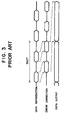
- Fig. 3 is a timing chart for reproducing PCM signals recorded as in Fig. 2.
- PCM signals of two tracks are reproduced every time the two rotary heads rotate once as previously discussed.
- a PCM signal reproduced is temporarily stored in a memory circuit, such as a RAM and thereafter, subjected to error correction and converted into an analog signal to output it.
- the PCM signal after error correction is once stored in another memory circuit similar to the above-described RAM where a parity (error correcting code) shown by numeral 33 in Fig. 2 is added.
- An object of these present invention is to provide a PCM signal recording and reproducing apparatus capable of copying PCM signals, not requiring the addition of an error detection code in copying, which is relatively inexpensive.
- two memory circuits are used. While PCM signals are read and written using one of the two memory circuits, PCM signals stored in the other memory circuit are error-corrected. At the end of writing with respect to the former memory circuits are interchanged to read the error-corrected PCM signals stored in the latter memory circuit. The readout error-corrected PCM signals are then recorded on another magnetic tape, thus dispensing with a parity adding circuit necessary for recording, and realizing inexpensive copying. Further, a high speed copying is possible without incorporating a high speed access to memory circuits.
- a first rotary head 3 has two magnetic heads 3b and 3c mounted on the periphery of a rotary member 3a, the heads being angularly spaced apart by 180 degrees.
- the magnetic tape 1 is slantwise wound about the periphery of the rotary member 3a over the angular range of 90 degrees, and disposed so as to alternately contact the two magnetic heads 3b and 3c.
- a second rotary head 4 has two magnetic heads 4b and 4c mounted on the periphery of a rotary member 4a, the heads being angularly spaced apart by 180 degrees.
- the magnetic tape 2 is slantwise wound about the periphery of the rotary member 4a over the angular range of 90 degrees, and disposed so as to alternately contact the two magnetic heads 4b and 4c.
- Other circuit elements include a reproducing amplifier 5, a recording amplifier 6, a recording/reproducing circuit 7, switching circuits 8 and 9, RAMs 10 and 11, an error correcting circuit 12, and a timing control circuit 13.
- a signal reproduced by the first rotary head 3 from the first magnetic tape 1 is amplified, waveform-equalized and converted into a digital signal by the reproducing amplifier 5.
- the digital signal is then inputted to a demodulation circuit 15 and a synchronizing signal detection circuit 16.
- the demodulation circuit 15 demodulates a PCM signal and a parity from the reproduced signal outputted by the reproducing amplifier 5.
- the synchronizing signal detection circuit 16 detects synchronizing signals in the reproduced signal.
- a write address generation circuit 17 generates an address indicative of the area of RAM 10 or RAM 11 where the PCM signal and the parity are written, based on the synchronizing signals detected by the synchronizing signal detection circuit 16 by the demodulation circuit 15 which also demodulated the PCM signal.
- the PCM signal and the parity demodulated by the demodulation circuit 15 are written in a first memory circuit or RAM 10 or a second memory circuit or RAM 11 in accordance with the generated address.
- the control signals in the reproduced signal are detected by the control signal detection circuit 18 and temporarily stored in this circuit.
- a modulation circuit 20 modulates the PCM signal and the parity read from either RAM 10 or RAM 11 in accordance with an address generated by a read address generating circuit 21, and modulates also the control signals stored in the control signal detecting circuit 18. These modulated signals, together with the synchronizing signals generated by the synchronizing signal generating circuit 19, are recorded on the second magnetic tape 2 using the second rotary head 4.
- a buffer 22 is used in switching input and output operations with respect to RAMs 10 and 11, and a multiplexer 23 is for switching addresses of RAMs 10 and 11.
- the PCM signal and the parity which are read from RAM 10 or RAM 11 in accordance with an address generated by an error correction address generating circuit 25, are inputted via a switching circuit 9 to an error correcting circuit 24 to perform error correction.
- the error-corrected PCM signal and parity are again written in RAM 10 or RAM 11 for completing error correction.
- the timing control circuit 13 is for controlling switching timings of the switching circuits 8 and 9, i.e., switching timings of recording, reproducing, error-correcting, and RAMs 10 and 11.
- the switching circuits 8 and 9 are for switching data input/output and addresses with respect to RAMs 10 and 11, at the timings in units of 180 degrees, and are controlled by the timing control circuit 13.
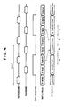
- the timing control circuit 13 itself is known as disclosed in the JP-A-59-16111. For instance, clocks from a clock generator are supplied to an address counter whose output is supplied to a ROM. The output from the ROM reverses its state at 30 Hz between the 180 degree rotating period of the rotary head 3 and that of the rotary head 4. In this embodiment, such a reversing signal is used as a RAM switching signal. In response to the RAM switching signal, if one of the switching circuits 8 and 9 selects RAM 10, then the other of the switching circuits 8 and 9 selects RAM 11.
- the switching circuit 8 is selecting RAM 10 during which one track data is reproduced from the magnetic tape 1 at timing a.
- the reproduced PCM signal and parity are written in RAM 10.
- the switching circuits 8 and 9 are interchanged. That is, the switching circuit 9 selects this time RAM 10 so that at timings b and c PCM signal written at timing a is error-corrected using the parity.
- the switching circuit 8 is selecting RAM 11 so that at timing b the error-corrected PCM signal and parity stored in RAM 11 are read and recorded on the magnetic tape 2 through the modulation circuit 20.
- the PCM signal and parity reproduced from the magnetic tape 1 are written in RAM 11.
- the switching circuits 8 and 9 are again interchanged and the switching circuit 8 selects RAM 10. Then, the error-corrected PCM signal and parity at timings b and c recorded on the second magnetic tape 2 through the modulation circuit 20. During this period, the switching circuit 9 is selecting RAM 11 and the PCM signal stored in RAM 11 is error-corrected.
- the angular phases of the rotary heads 3 and 4 are controlled so that the reproducing and the recording are alternately performed.
- a RAM switching signal is obtained from the ROM of the timing control circuit 13 as described before, a recording servo reference signal and a reproducing servo reference signal are also intended to be obtained from the ROM in this embodiment. Therefore, a minor change of the content of the ROM enables obtaining these reference signals for alternately using the rotary heads 3 and 4 for recording/reproducing.
- FIG. 5 Another embodiment of the present invention will be described with reference to Fig. 5.
- a circuit capable of outputting PCM signals in the form of sounds during a copying operation is added to the PCM signal recording and reproducing apparatus shown in Fig. 1.
- Additional elements include a D/A address generating circuit 40, a multiplexer 41, a latch circuit 42, and a D/A converter 43.
- the capacity of RAM 10 and RAM 11 of Fig. 1 suffices if it can store PCM signals and parities corresponding to one track. However, in the circuit of Fig. 5, the capacity of RAM 10 and RAM 11 is such that it can store PCM signals and parities corresponding to two tracks.
- the operation timings of RAMs and associated circuits will be described referring to Fig. 6.
- the timings of recording/reproducing and error correcting are the same as in the case of Fig. 4, however, in this embodiment the memory area of the RAM 10 and RAM 11 is divided into two areas to be alternately used. For instance, if read and write operations are performed for a first area of RAM 10 at timing e, then at timing gread and write operations are carried out for a second area of RAM 10. Error correction is carried out immediately after a write operation to the RAM 10.
- the PCM signal and parity written in the first area of RAM 10 at timing e are error-corrected at timing f. Thereafter, at a succeeding timing i the corrected PCM signal and parity are read and recorded.
- the output of PCM signals to the D/A converter 43 is effected from RAM selected by the switching circuit 9, i.e., from the same RAM associated with error correction. While error correction is carried out for the first area of RAM, the PCM signal stored in the second area of the same RAM is outputted to the D/A converter 43. Alternatively, while error correction is carried out for the second area, the PCM signal stored in the first area is outputted to the D/A converter 43.
- the PCM signal written at timing e for example is error-corrected at timing f and thereafter, outputted to the D/A converter 43 at timing h and read and recorded at timing i.
- the error-corrected PCM signal can be outputted to the D/A converter 43 prior to reading-out thereof so that the PCM signal can be outputted in the form of sound signal.
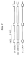
- Fig. 7 shows the output timing of PCM signals to the D/A converter 43.
- PCM signals can be outputted during the period between error corrections because the sampling frequency of PCM signals is in the order of 48 KHz. It is assumed here that the PCM signal is a two-channel signal of a sampling frequency 48 KHz and that the RAM access speed is 3.072 MHz (48 k x 64). Then, the output timing of PCM signals to the D/A converter 43 may be once per 32 slots of RAM access. For instance, during 4 slots among 32 slots PCM signals are outputted to the D/A converter 43, while on the other hand, the input/output operation with respect to the error correcting circuit 12 is carried out during the remaining 28 slots.
- the multiplexer 41 selects the D/A address generating circuit 40 to input an address of PCM signals, to be outputted to the D/A converter 43, to RAM 10 or RAM 11. During the remaining 28 slots, the multiplexer 41 selects the error correcting circuit 12 to input PCM signals and parities thereto or output them therefrom.
- the PCM signal read from RAM or RAM 11 in accordance with an address generated from the D/A address generating circuit 40 is latched by the latch circuit 42 and thereafter, inputted to the D/A converter 43 and converted into an analog signal which in turn is outputted from an output terminal 44.
- PCM signals can be outputted in the from of sound during a copying operation.
- PCM signals can be outputted in the form of sound during a high-speed copying.
- Figs. 8A and 8B show waveforms of output sounds during a double-speed copying.
- Fig. 8A shows a waveform of a PCM signal outputted from the D/A converter 43 at timings e to h.
- the front halves of the PCM signal at respective timings are sampled as shown in Fig. 8B to obtain a new PCM signal which in turn is converted into an analog signal at the same conversion period as in the ordinary reproduction.
- sounds during a double-speed copying can be outputted without raising the sound frequency.
- the flag may be stored in a specific area provided in RAM 10 or RAM 11, or in a memory circuit provided in the error correcting circuit 12.
Landscapes
- Engineering & Computer Science (AREA)
- Signal Processing (AREA)
- Multimedia (AREA)
- Signal Processing For Digital Recording And Reproducing (AREA)
- Digital Magnetic Recording (AREA)
Description
- The present invention relates to PCM signal recording and reproduction, and more particularly to a PCM signal recording and reproducing apparatus suitable for copying PCM signals.
- Of PCM signal recording and reproducing apparatus, there is disclosed in JP-A-59-16111 laid-open on January 27, 1984 (Japanese Patent Application No. 57-125565 filed on July 19, 1982) a rotary head type PCM recorder which records PCM signals on a magnetic tape using a rotary head. In the case where a rotary head type PCM recorder having a plurality of rotary heads, for example, two rotary heads, is used, the two heads are mounted on a rotary member each angularly spaced apart by 360°/2 = 180°. A magnetic tape is slantwise wound about the periphery of the rotary member over an angular range less than 180 degrees, for example, 90 degrees. The rotary member is then rotated while the magnetic tape is run in one direction. Then, PCM signals are recorded one track after another on the magnetic tape in the direction slanted relative to the longitudinal direction thereof alternately using the two heads, or PCM signals already recorded on the magnetic tape are reproduced using the two heads.
- PCM recorders of this type are advantageous in that high fidelity audio signals can be recorded and reproduced and that signal quality is not degraded even after plural copies. However, the conventional PCM recorders record or reproduce PCM signals using only one magnetic tape, as in the case of the JP-A-59-16111. Therefore, two PCM recorders have been required for copying recorded PCM signals; one for reproducing PCM signals recorded on a magnetic tape, and the other for recording the reproduced PCM signals on another magnetic tape. Further, a high speed copying such as a double speed copying has not been considered.
- Fig. 2 shows an example of a record pattern on a magnetic tape recorded by a conventional single PCM recorder of a rotary head type.
Reference numeral 1 generally represents a magnetic tape, andreference numeral 30 represents one block. One track is constructed of a plurality of blocks, for example, 128 blocks, including synchronizingsignals 31,control signals 32 such as signals associated with PCM signals and a block number, and PCM signals and error correcting code 33 (the latter is used for correcting errors and called parity hereinafter). The format of one block data is disclosed in the JP-A-5916111. - Fig. 3 is a timing chart for reproducing PCM signals recorded as in Fig. 2. With rotary head type PCM recorders as disclosed in JP-A-59-16111, PCM signals of two tracks are reproduced every time the two rotary heads rotate once as previously discussed. A PCM signal reproduced is temporarily stored in a memory circuit, such as a RAM and thereafter, subjected to error correction and converted into an analog signal to output it. In order to copy the reproduced PCM signal, the PCM signal after error correction is once stored in another memory circuit similar to the above-described RAM where a parity (error correcting code) shown by
numeral 33 in Fig. 2 is added. Thereafter, the PCM signal with a parity is applied to a modulating circuit and recorded on another magnetic tape using other rotary heads. Consequently, there arises a problem that the conventional apparatus become expensive. Further, in case of a high speed copying, reproduction, error correction and recording must be carried out at high speed so that signal processing circuits and recording circuits must be accessed at high speed. For instance, in case of a double speed copying, the time required for reproducing and error-correcting PCM signals becomes half, respectively. Moreover, a time for recording is needed so that memory circuits and signal processing circuits must be operated at a double speed or higher. Particularly, in case of error correction, it is necessary to input data from a memory circuit to an error correcting circuit and write the corrected data in another memory circuit, thus causing a number of accesses to RAMs and therefore leaving only a short time for error correction. - A PCM signal recording and reproducing apparatus is disclosed in JP-A 60-15 826 laid open on January 26, 1985 (Japanese patent Application No. 58-124 313 filed on July 7, 1983), requiring the addition of an error detection code in copying.
- An object of these present invention is to provide a PCM signal recording and reproducing apparatus capable of copying PCM signals, not requiring the addition of an error detection code in copying, which is relatively inexpensive.
- The above object is achieved by the apparatus defined in
claim 1. - According to one feature of the present invention, two memory circuits (RAMs) are used. While PCM signals are read and written using one of the two memory circuits, PCM signals stored in the other memory circuit are error-corrected. At the end of writing with respect to the former memory circuits are interchanged to read the error-corrected PCM signals stored in the latter memory circuit. The readout error-corrected PCM signals are then recorded on another magnetic tape, thus dispensing with a parity adding circuit necessary for recording, and realizing inexpensive copying. Further, a high speed copying is possible without incorporating a high speed access to memory circuits.
-
- Fig. 1 is a circuit diagram of the PCM signal recording and reproducing apparatus according to an embodiment of the present invention.
- Fig. 2 is an example of a record pattern on a magnetic tape.
- Fig. 3 is a timing chart for reproducing operation according to the prior art.
- Fig. 4 is a timing chart for the circuit of Fig. 1.
- Fig. 5 is a circuit diagram of the PCM signal recording and reproducing apparatus according to another embodiment of the present invention.
- Fig. 6 is a timing chart for the circuit of Fig. 5.
- Fig. 7 is a timing chart for D/A converter output.
- Figs. 8A and 8B are waveforms of analog signals during a double-speed copying.
- First, an embodiment of the present invention will be described with reference to Fig. 1.
- In the circuit shown in Fig. 1, PCM signals recorded on a first
magnetic tape 1 are copied on a secondmagnetic tape 2. A first rotary head 3 has twomagnetic heads rotary member 3a, the heads being angularly spaced apart by 180 degrees. Themagnetic tape 1 is slantwise wound about the periphery of therotary member 3a over the angular range of 90 degrees, and disposed so as to alternately contact the twomagnetic heads rotary head 4 has twomagnetic heads 4b and 4c mounted on the periphery of arotary member 4a, the heads being angularly spaced apart by 180 degrees. Themagnetic tape 2 is slantwise wound about the periphery of therotary member 4a over the angular range of 90 degrees, and disposed so as to alternately contact the twomagnetic heads 4b and 4c. Other circuit elements include a reproducing amplifier 5, arecording amplifier 6, a recording/reproducing circuit 7,switching circuits 8 and 9,RAMs 10 and 11, anerror correcting circuit 12, and atiming control circuit 13. - In the operation of reproducing, a signal reproduced by the first rotary head 3 from the first
magnetic tape 1 is amplified, waveform-equalized and converted into a digital signal by the reproducing amplifier 5. The digital signal is then inputted to a demodulation circuit 15 and a synchronizingsignal detection circuit 16. The demodulation circuit 15 demodulates a PCM signal and a parity from the reproduced signal outputted by the reproducing amplifier 5. The synchronizingsignal detection circuit 16 detects synchronizing signals in the reproduced signal. A writeaddress generation circuit 17 generates an address indicative of the area ofRAM 10 or RAM 11 where the PCM signal and the parity are written, based on the synchronizing signals detected by the synchronizingsignal detection circuit 16 by the demodulation circuit 15 which also demodulated the PCM signal. The PCM signal and the parity demodulated by the demodulation circuit 15 are written in a first memory circuit orRAM 10 or a second memory circuit or RAM 11 in accordance with the generated address. The control signals in the reproduced signal are detected by the controlsignal detection circuit 18 and temporarily stored in this circuit. - In the operation of recording, a
modulation circuit 20 modulates the PCM signal and the parity read from eitherRAM 10 or RAM 11 in accordance with an address generated by a readaddress generating circuit 21, and modulates also the control signals stored in the controlsignal detecting circuit 18. These modulated signals, together with the synchronizing signals generated by the synchronizingsignal generating circuit 19, are recorded on the secondmagnetic tape 2 using the secondrotary head 4. Abuffer 22 is used in switching input and output operations with respect toRAMs 10 and 11, and a multiplexer 23 is for switching addresses ofRAMs 10 and 11. - In the operation of error correction, the PCM signal and the parity, which are read from
RAM 10 or RAM 11 in accordance with an address generated by an error correctionaddress generating circuit 25, are inputted via a switching circuit 9 to anerror correcting circuit 24 to perform error correction. The error-corrected PCM signal and parity are again written inRAM 10 or RAM 11 for completing error correction. Thetiming control circuit 13 is for controlling switching timings of theswitching circuits 8 and 9, i.e., switching timings of recording, reproducing, error-correcting, andRAMs 10 and 11. - In the operation of copying PCM signals recorded on the
magnetic tape 1 to themagnetic tape 2, a signal reproduced from themagnetic tape 1 is stored inRAM 10 or RAM 11 and thereafter error-corrected. Then, the corrected signal is again read fromRAM 10 or RAM 11 to record it on themagnetic tape 2. In this case, by alternately usingRAMs 10 and 11 between read/write and error-correction, and access speed to RAMs and associated circuits will be lowered. Further, since there is provided only one set of the recording/reproducing circuit and the error correcting circuit, the scale of circuits will not become large. In particular, parities corrected during error correction are retained so that copying can be performed after error correction using the retained parities without newly generating parities. - The operation timings of RAMs and associated circuits will now be described with reference to Fig. 4.
- As described previously, PCM signals of two tracks are reproduced every time the rotary head rotates once (360 degrees). Since the wound-angle of the magnetic tape about the rotary head is 90 degrees, PCM signals of one track are reproduced by one fourth (90 degrees) of a single revolution. The switching
circuits 8 and 9 are for switching data input/output and addresses with respect toRAMs 10 and 11, at the timings in units of 180 degrees, and are controlled by thetiming control circuit 13. Thetiming control circuit 13 itself is known as disclosed in the JP-A-59-16111. For instance, clocks from a clock generator are supplied to an address counter whose output is supplied to a ROM. The output from the ROM reverses its state at 30 Hz between the 180 degree rotating period of the rotary head 3 and that of therotary head 4. In this embodiment, such a reversing signal is used as a RAM switching signal. In response to the RAM switching signal, if one of the switchingcircuits 8 and 9 selectsRAM 10, then the other of the switchingcircuits 8 and 9 selects RAM 11. - Assume that the
switching circuit 8 is selectingRAM 10 during which one track data is reproduced from themagnetic tape 1 at timing a. The reproduced PCM signal and parity are written inRAM 10. After the reproduced signal is written, the switchingcircuits 8 and 9 are interchanged. That is, the switching circuit 9 selects thistime RAM 10 so that at timings b and c PCM signal written at timing a is error-corrected using the parity. At this period, the switchingcircuit 8 is selecting RAM 11 so that at timing b the error-corrected PCM signal and parity stored in RAM 11 are read and recorded on themagnetic tape 2 through themodulation circuit 20. At timing c, the PCM signal and parity reproduced from themagnetic tape 1 are written in RAM 11. At timing d, the switchingcircuits 8 and 9 are again interchanged and theswitching circuit 8 selectsRAM 10. Then, the error-corrected PCM signal and parity at timings b and c recorded on the secondmagnetic tape 2 through themodulation circuit 20. During this period, the switching circuit 9 is selecting RAM 11 and the PCM signal stored in RAM 11 is error-corrected. - As described above, by alternately switching
RAM 10 and RAM 11 between recording/reproducing and error correcting, access to each RAM is performed either for recording/reproducing or for error correcting so that copying can be carried out without raising the access speed. Further, a high speed copying is also possible if the access speed is raised. For instance, assuming that the transfer rate of a reproduced signal is 1 MBPS (mega-byte/sec, the same rate is assumed for recording), a double speed copying is possible if the access speed to RAMs is set as twice higher than 2 MHz or more. For error correction, one error correction will suffice during 180 degree rotation. Therefore, an error correction is ensured if an access to RAMs is performed at the same access speed as that of recording/reproducing. - As to the timings for reproducing/recording of PCM signals, the angular phases of the rotary heads 3 and 4 are controlled so that the reproducing and the recording are alternately performed. In particular, although a RAM switching signal is obtained from the ROM of the
timing control circuit 13 as described before, a recording servo reference signal and a reproducing servo reference signal are also intended to be obtained from the ROM in this embodiment. Therefore, a minor change of the content of the ROM enables obtaining these reference signals for alternately using the rotary heads 3 and 4 for recording/reproducing. - Another embodiment of the present invention will be described with reference to Fig. 5. In the circuit shown in Fig. 5, a circuit capable of outputting PCM signals in the form of sounds during a copying operation is added to the PCM signal recording and reproducing apparatus shown in Fig. 1.
- Additional elements include a D/A
address generating circuit 40, amultiplexer 41, alatch circuit 42, and a D/A converter 43. The capacity ofRAM 10 and RAM 11 of Fig. 1 suffices if it can store PCM signals and parities corresponding to one track. However, in the circuit of Fig. 5, the capacity ofRAM 10 and RAM 11 is such that it can store PCM signals and parities corresponding to two tracks. - The operation timings of RAMs and associated circuits will be described referring to Fig. 6. The timings of recording/reproducing and error correcting are the same as in the case of Fig. 4, however, in this embodiment the memory area of the
RAM 10 and RAM 11 is divided into two areas to be alternately used. For instance, if read and write operations are performed for a first area ofRAM 10 at timing e, then at timing gread and write operations are carried out for a second area ofRAM 10. Error correction is carried out immediately after a write operation to theRAM 10. In particular, the PCM signal and parity written in the first area ofRAM 10 at timing e are error-corrected at timing f. Thereafter, at a succeeding timing i the corrected PCM signal and parity are read and recorded. - The output of PCM signals to the D/
A converter 43 is effected from RAM selected by the switching circuit 9, i.e., from the same RAM associated with error correction. While error correction is carried out for the first area of RAM, the PCM signal stored in the second area of the same RAM is outputted to the D/A converter 43. Alternatively, while error correction is carried out for the second area, the PCM signal stored in the first area is outputted to the D/A converter 43. As a result, the PCM signal written at timing e for example, is error-corrected at timing f and thereafter, outputted to the D/A converter 43 at timing h and read and recorded at timing i. As such, the error-corrected PCM signal can be outputted to the D/A converter 43 prior to reading-out thereof so that the PCM signal can be outputted in the form of sound signal. - Fig. 7 shows the output timing of PCM signals to the D/
A converter 43. PCM signals can be outputted during the period between error corrections because the sampling frequency of PCM signals is in the order of 48 KHz. It is assumed here that the PCM signal is a two-channel signal of a sampling frequency 48 KHz and that the RAM access speed is 3.072 MHz (48 k x 64). Then, the output timing of PCM signals to the D/A converter 43 may be once per 32 slots of RAM access. For instance, during 4 slots among 32 slots PCM signals are outputted to the D/A converter 43, while on the other hand, the input/output operation with respect to theerror correcting circuit 12 is carried out during the remaining 28 slots. During 4 slots for outputting PCM signals to the D/A converter 43, themultiplexer 41 selects the D/Aaddress generating circuit 40 to input an address of PCM signals, to be outputted to the D/A converter 43, to RAM 10 or RAM 11. During the remaining 28 slots, themultiplexer 41 selects theerror correcting circuit 12 to input PCM signals and parities thereto or output them therefrom. The PCM signal read from RAM or RAM 11 in accordance with an address generated from the D/Aaddress generating circuit 40 is latched by thelatch circuit 42 and thereafter, inputted to the D/A converter 43 and converted into an analog signal which in turn is outputted from anoutput terminal 44. - As above, PCM signals can be outputted in the from of sound during a copying operation. Obviously, PCM signals can be outputted in the form of sound during a high-speed copying.
- Figs. 8A and 8B show waveforms of output sounds during a double-speed copying. Fig. 8A shows a waveform of a PCM signal outputted from the D/
A converter 43 at timings e to h. In order to obtain an analog signal corresponding to the PCM signal, it is necessary to double the conversion period of the D/A converter 43, resulting in an indistinct sound having a frequency twice as high as in an ordinary speed copying. In view of this, the front halves of the PCM signal at respective timings are sampled as shown in Fig. 8B to obtain a new PCM signal which in turn is converted into an analog signal at the same conversion period as in the ordinary reproduction. With this analog signal, sounds during a double-speed copying can be outputted without raising the sound frequency. - It is necessary to add a flag to a PCM signal, during error correction and sound outputting, for indicating that error correction is being carried out or error is incorrectable. To this end, the flag may be stored in a specific area provided in
RAM 10 or RAM 11, or in a memory circuit provided in theerror correcting circuit 12.
Claims (5)
Applications Claiming Priority (2)
| Application Number | Priority Date | Filing Date | Title |
|---|---|---|---|
| JP158124/85 | 1985-07-19 | ||
| JP60158124A JPS6220180A (en) | 1985-07-19 | 1985-07-19 | Pcm signal recording and reproducing device |
Publications (3)
| Publication Number | Publication Date |
|---|---|
| EP0209141A2 EP0209141A2 (en) | 1987-01-21 |
| EP0209141A3 EP0209141A3 (en) | 1987-07-22 |
| EP0209141B1 true EP0209141B1 (en) | 1989-12-20 |
Family
ID=15664816
Family Applications (1)
| Application Number | Title | Priority Date | Filing Date |
|---|---|---|---|
| EP86109836A Expired EP0209141B1 (en) | 1985-07-19 | 1986-07-17 | Pcm signal recording and reproducing apparatus |
Country Status (5)
| Country | Link |
|---|---|
| US (1) | US4758902A (en) |
| EP (1) | EP0209141B1 (en) |
| JP (1) | JPS6220180A (en) |
| KR (1) | KR900006566B1 (en) |
| DE (1) | DE3667739D1 (en) |
Families Citing this family (24)
| Publication number | Priority date | Publication date | Assignee | Title |
|---|---|---|---|---|
| JPS6278779A (en) * | 1985-10-02 | 1987-04-11 | Hitachi Ltd | Recording and reproducing device for pcm signal |
| JPH0650870Y2 (en) * | 1986-09-19 | 1994-12-21 | パイオニア株式会社 | Information recording / reproducing device |
| JPS6390007A (en) * | 1986-10-02 | 1988-04-20 | Victor Co Of Japan Ltd | Rotary head type digital signal recording/reproducing device |
| US4833549A (en) * | 1987-01-07 | 1989-05-23 | Casio Computer Co., Ltd. | Digital audio tape record/play-back system for recording/playing back character data together with digital audio data |
| DE3883641T2 (en) * | 1987-06-30 | 1993-12-16 | Toshiba Kawasaki Kk | Recording control device. |
| DE3889804T2 (en) * | 1987-08-12 | 1994-09-08 | Hitachi Ltd | Device for recording / playing back PCM signals. |
| US4872070A (en) * | 1987-09-11 | 1989-10-03 | Electro Sound, Inc. | System and method for high speed video tape reproduction |
| US4866543A (en) * | 1987-09-11 | 1989-09-12 | Electro Sound, Inc. | Multiple slave video tape reproduction system |
| JPS6489678A (en) * | 1987-09-30 | 1989-04-04 | Hitachi Ltd | Signal processing system |
| US4975835A (en) * | 1987-10-30 | 1990-12-04 | Casio Computer Co., Ltd. | Variable length data processing apparatus for consecutively processing variable-length data responsive to one instruction |
| US4899230A (en) * | 1987-12-22 | 1990-02-06 | Idb Corporation | Taped data copying utilizing multiple addressable memories |
| US4928280A (en) * | 1988-04-29 | 1990-05-22 | International Business Machines Corporation | Fast processor for multi-bit error correction codes |
| US5187589A (en) * | 1988-07-28 | 1993-02-16 | Pioneer Electronic Corporation | Multiprogram video tape recording and reproducing device |
| US5793547A (en) * | 1989-10-02 | 1998-08-11 | Canon Kabushiki Kaisha | Information signal reproducing apparatus with signal correcting function |
| US5247402A (en) * | 1989-11-14 | 1993-09-21 | Matsushita Electric Industrial Co., Ltd. | Apparatus for high speed searching and reproduction of data recorded in a tape medium |
| NL9001039A (en) * | 1990-05-01 | 1991-12-02 | Philips Nv | DEVICE FOR OBTAINING PRE-PLAYED DIGITAL MUSIC CASSETTES. |
| IT1243715B (en) * | 1990-08-31 | 1994-06-21 | Bernardino Bernardini | ELECTRONIC DEVICE FOR THE FAST DUPLICATION OF MAGNETIC TAPES |
| JP3120533B2 (en) * | 1992-02-12 | 2000-12-25 | ソニー株式会社 | Image recognition improvement circuit |
| DE69229440T2 (en) * | 1992-03-10 | 1999-10-07 | Hewlett Packard Ltd | Data storage device |
| JP3433811B2 (en) * | 1992-09-30 | 2003-08-04 | ソニー株式会社 | Disk duplication device |
| JPH06162743A (en) * | 1992-11-13 | 1994-06-10 | Sony Corp | Method and device for optical disk reproducing |
| JP3340783B2 (en) * | 1993-03-24 | 2002-11-05 | 富士通株式会社 | Disk controller |
| US5699370A (en) * | 1994-02-17 | 1997-12-16 | Hitachi, Ltd. | Information recording and reproduction apparatus to be controlled by temporal information |
| US5515387A (en) * | 1994-12-12 | 1996-05-07 | Trw Inc. | Signal independent pulse code modulation data enhancer and associated method |
Family Cites Families (11)
| Publication number | Priority date | Publication date | Assignee | Title |
|---|---|---|---|---|
| JPS54137204A (en) * | 1978-04-17 | 1979-10-24 | Sony Corp | Digital signal transmission method |
| JPS57132486A (en) * | 1981-02-10 | 1982-08-16 | Sony Corp | Magnetic recorder and reproducer |
| JPS58143410A (en) * | 1982-02-18 | 1983-08-26 | Sony Corp | Copying method for video tape |
| JPS58179913A (en) * | 1982-04-15 | 1983-10-21 | Sony Corp | Recorder of audio signal |
| JPS591611A (en) * | 1982-06-28 | 1984-01-07 | Nisshin Steel Co Ltd | Treatment of dust from steel making furnace |
| JPS5916111A (en) * | 1982-07-19 | 1984-01-27 | Sony Corp | Recording and reproducing device of pcm signal |
| JPS59119519A (en) * | 1982-12-27 | 1984-07-10 | Sony Corp | Recorder of pcm signal |
| JPS59124010A (en) * | 1982-12-29 | 1984-07-18 | Sony Corp | Recording method of pcm signal |
| US4628373A (en) * | 1983-06-10 | 1986-12-09 | Hitachi, Ltd. | Rotating head type magnetic record/reproduce apparatus |
| JPS6015826A (en) * | 1983-07-06 | 1985-01-26 | Mitsubishi Electric Corp | Video recording and reproducing device |
| JPH0634314B2 (en) * | 1983-12-22 | 1994-05-02 | 松下電器産業株式会社 | Video signal recording / reproducing device |
-
1985
- 1985-07-19 JP JP60158124A patent/JPS6220180A/en active Pending
-
1986
- 1986-07-16 KR KR1019860005739A patent/KR900006566B1/en not_active IP Right Cessation
- 1986-07-16 US US06/886,235 patent/US4758902A/en not_active Expired - Fee Related
- 1986-07-17 EP EP86109836A patent/EP0209141B1/en not_active Expired
- 1986-07-17 DE DE8686109836T patent/DE3667739D1/en not_active Expired - Lifetime
Also Published As
| Publication number | Publication date |
|---|---|
| US4758902A (en) | 1988-07-19 |
| KR900006566B1 (en) | 1990-09-13 |
| EP0209141A2 (en) | 1987-01-21 |
| DE3667739D1 (en) | 1990-01-25 |
| JPS6220180A (en) | 1987-01-28 |
| KR870001579A (en) | 1987-03-14 |
| EP0209141A3 (en) | 1987-07-22 |
Similar Documents
| Publication | Publication Date | Title |
|---|---|---|
| EP0209141B1 (en) | Pcm signal recording and reproducing apparatus | |
| JP2574744B2 (en) | PCM signal recording / reproducing device | |
| KR850006958A (en) | Rotary head type PCM recording and playback method and system | |
| US5155636A (en) | Apparatus and method for recording and reproducing digital data | |
| JPS607651A (en) | Recording device of digital information signal | |
| JPH0357527B2 (en) | ||
| JPH0580749B2 (en) | ||
| JPH03119573A (en) | Magnetic recording and reproducing device | |
| JPH0661154B2 (en) | PCM signal recorder | |
| JPH0542069B2 (en) | ||
| JP2537903B2 (en) | Magnetic recording / reproducing device | |
| JPH0697543B2 (en) | Recording device for PCM data | |
| JPS6278779A (en) | Recording and reproducing device for pcm signal | |
| JPH0782713B2 (en) | PCM signal recording / reproducing apparatus and reproducing apparatus | |
| JP2576509B2 (en) | Data recorder | |
| JP3044845B2 (en) | Information playback device | |
| JPH09259528A (en) | Magnetic disk apparatus | |
| JPS63251971A (en) | Data recorder | |
| JP2616420B2 (en) | Magnetic playback device | |
| JP2542831B2 (en) | Rotating head type recording / reproducing device | |
| JPH0697538B2 (en) | Digital signal recording / reproducing device | |
| JP2576535B2 (en) | Data recorder | |
| JP2703935B2 (en) | Video data playback device | |
| JPH0782712B2 (en) | Digital signal recording / reproducing device | |
| EP0449213A2 (en) | Interleave address generating circuit of digital audio tape recorder |
Legal Events
| Date | Code | Title | Description |
|---|---|---|---|
| PUAI | Public reference made under article 153(3) epc to a published international application that has entered the european phase |
Free format text: ORIGINAL CODE: 0009012 |
|
| 17P | Request for examination filed |
Effective date: 19860717 |
|
| AK | Designated contracting states |
Kind code of ref document: A2 Designated state(s): DE FR GB |
|
| PUAL | Search report despatched |
Free format text: ORIGINAL CODE: 0009013 |
|
| AK | Designated contracting states |
Kind code of ref document: A3 Designated state(s): DE FR GB |
|
| 17Q | First examination report despatched |
Effective date: 19880208 |
|
| GRAA | (expected) grant |
Free format text: ORIGINAL CODE: 0009210 |
|
| AK | Designated contracting states |
Kind code of ref document: B1 Designated state(s): DE FR GB |
|
| REF | Corresponds to: |
Ref document number: 3667739 Country of ref document: DE Date of ref document: 19900125 |
|
| ET | Fr: translation filed | ||
| PLBE | No opposition filed within time limit |
Free format text: ORIGINAL CODE: 0009261 |
|
| STAA | Information on the status of an ep patent application or granted ep patent |
Free format text: STATUS: NO OPPOSITION FILED WITHIN TIME LIMIT |
|
| 26N | No opposition filed | ||
| PGFP | Annual fee paid to national office [announced via postgrant information from national office to epo] |
Ref country code: FR Payment date: 19950516 Year of fee payment: 10 |
|
| PGFP | Annual fee paid to national office [announced via postgrant information from national office to epo] |
Ref country code: GB Payment date: 19950707 Year of fee payment: 10 |
|
| PGFP | Annual fee paid to national office [announced via postgrant information from national office to epo] |
Ref country code: DE Payment date: 19950825 Year of fee payment: 10 |
|
| PG25 | Lapsed in a contracting state [announced via postgrant information from national office to epo] |
Ref country code: GB Effective date: 19960717 |
|
| GBPC | Gb: european patent ceased through non-payment of renewal fee |
Effective date: 19960717 |
|
| PG25 | Lapsed in a contracting state [announced via postgrant information from national office to epo] |
Ref country code: FR Effective date: 19970328 |
|
| PG25 | Lapsed in a contracting state [announced via postgrant information from national office to epo] |
Ref country code: DE Effective date: 19970402 |
|
| REG | Reference to a national code |
Ref country code: FR Ref legal event code: ST |