EP0209014A2 - Arrangement having a saturable carry-save adder - Google Patents
Arrangement having a saturable carry-save adder Download PDFInfo
- Publication number
- EP0209014A2 EP0209014A2 EP86109135A EP86109135A EP0209014A2 EP 0209014 A2 EP0209014 A2 EP 0209014A2 EP 86109135 A EP86109135 A EP 86109135A EP 86109135 A EP86109135 A EP 86109135A EP 0209014 A2 EP0209014 A2 EP 0209014A2
- Authority
- EP
- European Patent Office
- Prior art keywords
- carry
- adders
- inputs
- bits
- subtotal
- Prior art date
- Legal status (The legal status is an assumption and is not a legal conclusion. Google has not performed a legal analysis and makes no representation as to the accuracy of the status listed.)
- Granted
Links
Images


Classifications
-
- G—PHYSICS
- G06—COMPUTING; CALCULATING OR COUNTING
- G06F—ELECTRIC DIGITAL DATA PROCESSING
- G06F7/00—Methods or arrangements for processing data by operating upon the order or content of the data handled
- G06F7/38—Methods or arrangements for performing computations using exclusively denominational number representation, e.g. using binary, ternary, decimal representation
- G06F7/48—Methods or arrangements for performing computations using exclusively denominational number representation, e.g. using binary, ternary, decimal representation using non-contact-making devices, e.g. tube, solid state device; using unspecified devices
- G06F7/50—Adding; Subtracting
- G06F7/505—Adding; Subtracting in bit-parallel fashion, i.e. having a different digit-handling circuit for each denomination
- G06F7/509—Adding; Subtracting in bit-parallel fashion, i.e. having a different digit-handling circuit for each denomination for multiple operands, e.g. digital integrators
- G06F7/5095—Adding; Subtracting in bit-parallel fashion, i.e. having a different digit-handling circuit for each denomination for multiple operands, e.g. digital integrators word-serial, i.e. with an accumulator-register
-
- G—PHYSICS
- G06—COMPUTING; CALCULATING OR COUNTING
- G06F—ELECTRIC DIGITAL DATA PROCESSING
- G06F7/00—Methods or arrangements for processing data by operating upon the order or content of the data handled
- G06F7/38—Methods or arrangements for performing computations using exclusively denominational number representation, e.g. using binary, ternary, decimal representation
- G06F7/48—Methods or arrangements for performing computations using exclusively denominational number representation, e.g. using binary, ternary, decimal representation using non-contact-making devices, e.g. tube, solid state device; using unspecified devices
- G06F7/499—Denomination or exception handling, e.g. rounding or overflow
- G06F7/49905—Exception handling
- G06F7/4991—Overflow or underflow
- G06F7/49921—Saturation, i.e. clipping the result to a minimum or maximum value
Definitions
- the invention relates to an arrangement with a carry-save adder for the bit-parallel addition of binary numbers in two's complement according to the preamble of patent claim 1.
- a carry-save adder of this type is known from the book "Computer Arithmetic" by K.Hwang, published by John Wiley & Sons, New York, 1979, pp. 98-103, in particular Fig. 4.2.
- each first adder has three inputs, each of which is assigned the equivalent bits of three binary numbers to be added together.
- the sum outputs of the first adders are led to first inputs of the adder, the carry outputs of the first adders (with the exception of the most significant adder) to second inputs of the adder.
- a sum word appears at the outputs of the latter as a result of the addition.
- a binary number is externally supplied to the third inputs of the first adders, while the first two inputs have a first intermediate result achieved by a previous addition, which consists of a subtotal word supplied to the first inputs and a carry word supplied to the second inputs at the outputs of the first adders, a second intermediate result formed by adding the first intermediate result and this number.
- the object of the present invention is to provide an arrangement of the type mentioned at the outset in which an overflow of the accumulated sum word is reliably avoided. This is achieved according to the invention by training according to the characterizing part of patent claim 1.
- the advantage that can be achieved with the invention is, in particular, that subtotals or Carry-over words that can lead to an overflow of the sum word are used immediately to identify an overflow situation and to eliminate it. This eliminates uncontrolled fluctuations in the summation word.
- FIG. 1 shows three adders AD n - 1 , AD n - 2 and AD " . 3 , each of which has three inputs, for example 1 to 3, for equivalent bits of three binary numbers to be added together, represented by two's complement, a sum output, for example 4, and have a carry output, for example 5.
- FIG. 1 is supplemented by further adders AD n - 4 ... AD., Which correspond to those shown in terms of structure and mode of operation AD are connected to output lines, for example 6 to 8, which are connected to first inputs 11, 12, 13 ...
- the adder AS has outputs 31, 32 ... 3n.
- AS consists, for example, of n adders AS n-1 ... AS o , each with three inputs and one output.
- the first two inputs of AS n-1 correspond to inputs 11 and 21 of AS
- the output of AS n-1 corresponds to output 31 of AS.
- AS n-2 has two inputs 12, 22 and output 32 etc.
- the third input of AS n- 1 is connected to the carry output of ASn-2, the third input of AS n-2 , not shown, to the carry output from AS n-3 etc.
- a recursive circuit branch 16 connects the output line 6 connected to the sum output of AD n-1 to the first input of this adder.
- a second recursive circuit branch 17 connects the output line 14 connected to the carry output 5 of AD n-2 to the second input of AD n-1.
- recursive circuit branches 18, 19 lead to the first two inputs 1, 2 of AD n-2 , as well as further recursive circuit branches to the first two inputs of the remaining adders AD 1 - Logic circuits 23 to 25 are inserted into the output lines 6 to 8, further logic circuits 26 and 27 are inserted into the output lines 14 and 15.
- the output lines 6 to 8, 14 and 15 each inserted intermediate memories, in particular shift registers, 33 to 37.
- the recursive circuit branches, for example 16, 17, are connected to the associated output lines, for example 6, 14, in such a way that the connection points are on the output side of the logic circuits 23 to 27 and the intermediate memories 33 to 37.
- a decoder 28 has four inputs 29, 30, 38 and 39, of which 29 and 30 with the first two inputs of AD n-1 and 38 and 39 with the first two inputs of AD n . 2 are connected.
- Outputs 40 and 40 'of 28 are connected to inputs of all logic circuits, for example 23 to 27.
- An output 41 of 28 is fed to the inputs of some logic circuits, for example 25, which are arranged downstream of the sum outputs of the adders AD 1 , while an output 42 is fed to the inputs of the other logic circuits, for example 23 and 24, which are connected to the sum outputs of AD; are subordinate.
- the number D is thus supplemented by doubling its sign bit to an n-digit number. If the logic circuits 23 to 27 are not taken into account, the bits d n-2, d n - 3 ... occur after performing a bit-parallel addition in the adders AD 1 also at the sum outputs thereof, whereby they are stored in the intermediate memories 33 to 35 can be registered.
- these bits are then switched through by the recursive circuit branches 16, 18 ... to the first inputs, for example 1, of AD, while at the same time a new binary number D1 is applied to the third inputs of AD i .
- a first intermediate result corresponding to the sum of D + D1 is obtained in the form of a subtotal word at the sum outputs and a carry word at the carry outputs of AD i .
- the bits of the subtotal word are written into the intermediate memories 33, 34 ..., the bits of the carry word into the intermediate memories 36, 37 ...
- the logic circuits for example 26, 27 ..., are expediently connected to the carry outputs of AD ; by the signals ORALL and
- ORALL causes the carry bits C n-1, C n-2 ... on the input side, which are otherwise connected to their outputs, to be switched off by them. Instead of these bits, saturation carry bits 0 are now output via the outputs of all of these logic circuits.
- the logic circuits 23, 24 are connected to the sum outputs of the two most significant adders AD n-1 and AD n-2 by means of the signals - OVFL , ORALL and ORALL influenced so that they turn off the input subtotal bits S n-1 and S n-2, which are otherwise connected to their outputs, switch them off and replace them with saturation subtotal bits of the value 0.
- ORALL and ORALL also cause the logic circuits, for example 25, at the sum outputs of the adders AD n-3 ... AD 0 to switch off the subtotal bits present on the input side, which are otherwise connected through to their outputs, and replace them with saturation subtotal bits of the value 1.
- the logic circuits 23, 24 are connected to the sum outputs of the two most significant adders AD n-1 and AD n . 2 by means of the signals ORALL, ORALL and -OVFL influenced in such a way that they switch off the subtotal bits S n-1 and S n-2 from the outputs and replace them with saturation subtotal bits of the value 1.
- ORALL and ORALL further cause the logic circuits, e.g. B. 25, at the sum outputs of the adders AD n-3 ... AD 0, switch off the subtotal bits on the input side of their outputs and replace each with saturation subtotal bits of the value 0.
- the saturation measures described above can be generalized to the effect that the output lines, for example 6 to 8 and 14, 15, at the outputs of the adders AD ; if overflow conditions occur, the subtotal and carry words S and C output via the adders AD j are activated and instead, predetermined saturation subtotals and carry carry words are applied.
- the subtotal saturation and carry-over saturation words should be selected such that they result in an accumulator word or sum word S ', the associated accumulator content of which comes as close as possible to a limit value to which the positive (negative) overflow condition already applies, without, however, reaching or exceeding this limit value, regardless of how the accumulator word is composed of the saturation subtotal and saturation carry word.
- condition mentioned above is the same for the number example given for a 5-bit accumulator with a saturation carry word of 0000 and a saturation subtotal word of 00111 A positive overflow condition and a saturation subtotal of 11000 occurred when a negative overflow condition occurred.
- Fig. 2 shows an embodiment of the decoder 28 of Fig. 1.
- the inputs 29 and 30 are connected to the inputs of an AND gate 44 and to the inputs of a NOR gate 45.
- the inputs 38 and 39 are connected to the inputs of a NAND gate 46 and to the inputs of an OR gate 47.
- the outputs of 44 and 46 are at the inputs of an AND gate 48, the outputs of 45 and 47 are at the inputs of an AND gate 49.
- the outputs of 48 and 49 are in turn at the inputs of an OR gate 50, whose output forms the output 40 of the decoder 28. From this one reaches the output 40 'via an inverter 51.
- the output of 49 is connected to an inverter 52, the output of which corresponds to the output 41 of the decoder.
- the output of 48 is connected to an inverter 53. whose output represents the output 42 of the decoder. If the outputs 29, 30, 38 and 39 are each assigned the bits S n-1, C n-1, S n-2 and C n-2 , the positive overflow signal + OVFL can be tapped at the output of the AND gate 49, at the output of 48 of the negative overflow signal -OVFL.
- the signal ORALL is then available at the output 40 of the OR gate 50 and the signal inverted for this purpose at the output 40 ' ORALL
- the inverted overflow signals occur at the outputs 41 and 42 OVFL and - OVFL on.
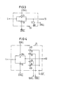
- FIG. 3 shows an exemplary embodiment of the logic circuit 26 which is connected downstream of the carry output 5 of AD n-2 .
- it contains two switching transistors 54 and 55 with their switching paths in parallel, the first of which is designed as a P-channel field-effect transistor and the second as an N-channel field-effect transistor.
- the source connections of these transistors are connected to the input of the logic circuit 26, which is connected to the carry output 5 of FIG. 1, the drain connections of these transistors to an output 56 of 26, which is connected to the input of the buffer 36.
- the output 56 is connected via a further N-channel switching transistor 57 to a switching point 58 which is at reference potential.
- the gates of 54 and 57 are assigned the ORALL signal, the gate of 55 the inverted signal ORALL .
- the other logic circuits, for example 27, which are connected downstream of the carry outputs of the adders AD n - 3 ... AD o are also expediently designed in accordance with FIG. 3.
- FIG. 4 An embodiment of the logic circuit 24 is shown in FIG. 4.
- two switching transistors 58a and 59 are provided with their switching paths in parallel, the source connections of which are connected to a switching point which is connected to the sum output 4 of AD n-2 .
- the drains of 58a and 59 are connected to a node 60, which is the output of 24.
- the circuit point 60 is connected via the series connection of two P-channel switching transistors 61 and 62 to a connection 63, which is connected to the supply voltage.
- 60 is connected to a connection 66 which is at reference potential via the series connection of two N-channel switching transistors 64 and 65.
- the gates of the P-channel transistor 58a and the transistor 64 are controlled via the output 40 with the signal ORALL, the gates of the N-channel transistor 59 and the transistor 62 with the signal which is output via the output 40 'and are inverted for this purpose
- ORALL The gates of 61 and 65 are connected to the output 42 of 28 and are connected with - OVFL acted upon.
- the logic circuit 23 is expediently also constructed in accordance with FIG. 4.
- the logic circuit 25 is advantageously constructed in accordance with FIG. 4, wherein only instead of the signal - OVFL the signal
- + OVFL is used to control the transistors 61 and 65.
- the logic circuits which are connected downstream of the sum outputs of the further adders AD n - 4 ... AD 0 are expediently likewise designed in accordance with the logic circuit 25.
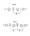
- FIG. 5 shows the development of an arrangement according to FIG. 1, which is used for the bit-parallel addition of four binary numbers in two's complement.
- the group of adders AD i already shown in FIG. 1 is followed by an additional group of adders ZA i , each adder ZA 1 being provided with three inputs.
- the output lines from AD I are omitted Logic circuits 23 to 27 and the latch 33 to 37 connected to the inputs of the adders ZA i .
- the output lines 6 to 8 are each led to the first inputs Z11, Z12 and Z13 of ZA n-1 , ZA n-2 and ZA n - 3 , the output lines 14 and 15 to the second inputs Z21 and Z22 of ZA n -1 and ZA n-2.
- the sum output of an adder AD with the first input of the adder ZA connected downstream; is connected while the carry output from AS; with the second input of the adder ZA i + 1 of the next higher value.
- the additional adders ZA are connected on their lower output sides in the same way and with the same circuit parts as the adders AD i in FIG. 1. These circuit parts are therefore provided with the same reference numerals as in FIG.
- the subtotal word occurring at points 11 ', 12' ..., which is applied to the first inputs of AD i via the intermediate memories 33 ', 34' ..., represents a first binary number, which appears at points 21 ', 22 '... occurring carry word, which is applied to the second inputs of AD i via the intermediate memories 36', 37 '..., a second binary number.
- the number D present at the third inputs of AD i forms a third binary number and a number E applied to the third inputs of the additional adders ZA i forms a fourth binary number.
- the decoder 28 in Depending on the bits at the first two inputs of AD n-1 and AD n-2, it is determined whether there is a positive or negative overflow condition and by means of the logic circuits 23 'to 27' etc., causes the saturation measures already explained with reference to FIG. 1.
- the arrangement according to FIG. 5 can be made in a corresponding manner by adding further adders ZA ; downstream groups of adders can be expanded for an addition of five or more binary numbers in two's complement.
- the circuit parts 23 'to 27' and 33 'to 37' are then provided on the output side by the further adders arranged in the lowest adder group and immediately preceding the adder AS '.
- the recursive circuit branches also run from the outputs of the intermediate memories 33' to 37 '. to the inputs of the adders AD. Circuit arrangements formed from a plurality of adder lines for adding five or more binary numbers are described, for example, in the book "Computer Arithmetic" by K.Hwang, published by John Wiley & Sons, New York, 1979, pp. 100-103, cf. in particular Fig. 4.3, removable.
- FIG. 6 shows a first-order recursive filter which contains an accumulator according to FIG. 1.
- a sequence of n-digit binary numbers Di which are respectively applied to the input 67 in successive clock periods and are represented in two's complement and correspond to a sequence of sampled amplitude values of an analog input signal, are initially bit-parallel by one in a delay stage 68, which consists of n buffers Delayed the cycle period and then supplied to the third inputs of the accumulator AD according to FIG. 1.
- the subtotals and carry words derived from this are delayed by a further clock period in a delay stage 69, which consists of the buffers 33 to 37, etc., and are then fed via a recursive loop 70 to the first and second inputs of the accumulator AD i . Both words can be shifted in their assignment to the individual adders AD i to the right or left by m bits, which corresponds to a multiplication by 2 -m or 2 m in an evaluator 70a. The more than 70 words supplied are added to the binary number D present at the third clock of AD i at the next clock cycle.
- the subtotal and carry words occurring at the output of delay stage 69 are fed to adder AS via their inputs 11, 12 ... 21, 22 ... and combined to form the filtered digital output signal Di '.
- FIG. 7 shows a recursive filter of the second order, which differs from FIG. 6 in that. that the subtotals and carry words given by 69 are fed to an accumulator according to FIG. 5, which is labeled AD ;, ZA; is indicated.
- the subtotals and carry words emitted by this are delayed by a clock period in a delay stage 71 (which corresponds to the buffers 33 'to 37') and via a recursive loop 72 both the first two inputs of the accumulator AD i and the first two inputs of the accumulator AD i , ZA i supplied.
- the third input of AD is assigned Di, the third and fourth inputs of AD ; , ZA i with the subtotal and carryover words of 69 of the first accumulator AD;
- the subtotals and carry words occurring at the output of the delay stage 71 are fed to the adder stage AS 'via their input 11', 12 '... 21', 22 'and combined to form the filtered digital output signal Di'.
- An accumulator according to FIG. 2 and n-1 accumulators according to FIG. 5 can be used in an analog manner in a recursive filter of the nth order.
- the buffers 33 to 37 or 33 'to 3T etc. can advantageously be designed as shift register stages, each consisting of master-slave flip-flops. Furthermore, the adding device AS or AS 'can be designed in accordance with the adding device shown in FIG. 9 of patent application P (VPA 85 P 1437 DE) and described in detail there.
- the adder AD n-1 can have a correction element on the output side which carries out an overflow correction which is necessary when relatively large sub-sum and carry words of opposite signs are combined to form a relatively small sum word.
- a correction element replaces the carry word of the adder AD n-2 with the second highest value by the carry bit of the most significant adder AD n-1 and in the event that the carry bits of the two most significant adders AD n-1 and AD n-2 are different the sum bit of AD n-1 is replaced by the carry bit of AD n-1 .
- Such overflow correction measures are described in detail in patent application P (VPA 85 P 1437 DE).
- each group in addition to the two most significant adders, for example AD n-1 and AD n-2, each group can also have other adders of subsequent valencies, for example AD n-3 and AD n-4, can each be assigned one and the same bit of a supplied binary number D or E via their third inputs. This then corresponds to a sign multiplication of the binary numbers represented in two's complement.
Landscapes
- Engineering & Computer Science (AREA)
- Physics & Mathematics (AREA)
- General Physics & Mathematics (AREA)
- Theoretical Computer Science (AREA)
- Pure & Applied Mathematics (AREA)
- Mathematical Analysis (AREA)
- Computational Mathematics (AREA)
- Computing Systems (AREA)
- Mathematical Optimization (AREA)
- General Engineering & Computer Science (AREA)
- Compression, Expansion, Code Conversion, And Decoders (AREA)
- Complex Calculations (AREA)
- Processing Of Color Television Signals (AREA)
Abstract
Anordnung mit einem sättigbaren Carry-Save-Addierer für eine bitparallele Addition von Binärzahlen im Zweierkomplement, bei der eine Reihe von Addierern (AD;) Zwischensummen-und Übertragsworte abgeben, die in einer Addiereinrichtung zu Summenworten zusammengesetzt werden. Zur Sättigung des Carry-Save-Addierers ist ein Dekoder (28) vorgesehen, der in Abhängigkeit von den beiden höchstwertigen Bits der Zwischensummen-und Übertragsworte Überlaufsignals erzeugt, durch die rekursive Schaltungszweige (16 bis 19) der Anordnung von den Zwischensummen-und Übertragsworten freigeschaltet und mit Sättigungszwischensummen-und
Sättigungsübertragsworten belegt werden. Diese ergeben Summenworte, die einen zulässigen Addiererinhalt nicht überschreiten.
Saturation transfer words are used. These result in sum words that do not exceed an admissible adder content.
Description
Die Erfindung bezieht sich auf eine Anordnung mit einem Carry-Save-Addierer zur bitparallelen Addition von Binärzahlen im Zweierkomplement nach dem Oberbegriff des Patentanspruchs 1.The invention relates to an arrangement with a carry-save adder for the bit-parallel addition of binary numbers in two's complement according to the preamble of
Ein Carry-Save-Addierer dieser Art ist aus dem Buch "Computer Arithmetic" von K.Hwang, Verlag John Wiley & Sons, New York, 1979, S. 98-103, insbesondere Fig. 4.2, bekannt. Hierbei weist jeder erste Addierer drei Eingänge auf, die jeweils mit gleichwertigen Bits dreier miteinander zu addierender Binärzahlen belegt sind. Die Summenausgänge der ersten Addierer sind an erste Eingänge der Addiereinrichtung geführt, die Übertragsausgänge der ersten Addierer (mit Ausnahme des höchstwertigen Addierers) an zweite Eingänge der Addiereinrichtung. An den Ausgängen der letzteren erscheint ein Summenwort als Ergebnis der Addition. Zum Unterschied von einer Addiereranordnung mit Übertragsdurchlauf ("Carry-Propagate"-Prinzip) werden hier die Überträge aller ersten Addierer bei einer Addition von drei Binärzahlen gleichzeitig gebildet und stehen als Übertragswort neben dem an den ersten Addierem abgegriffenen Zwischensummenwort für eine Addition in der Addiereinrichtung zur Verfügung. Ein in dieser Weise aufgebauter Addierer arbeitet nach dem sog. "Carry-Save"-Prinzip.A carry-save adder of this type is known from the book "Computer Arithmetic" by K.Hwang, published by John Wiley & Sons, New York, 1979, pp. 98-103, in particular Fig. 4.2. In this case, each first adder has three inputs, each of which is assigned the equivalent bits of three binary numbers to be added together. The sum outputs of the first adders are led to first inputs of the adder, the carry outputs of the first adders (with the exception of the most significant adder) to second inputs of the adder. A sum word appears at the outputs of the latter as a result of the addition. In contrast to an adder arrangement with carry-through ("carry-propagate" principle), the carry-overs of all first adders are formed simultaneously with an addition of three binary numbers and are available as a carry word in addition to the subtotal word picked up at the first adder for addition in the adder Available. An adder constructed in this way works according to the so-called "carry-save" principle.
Wird hierbei eine binäre Zahl den dritten Eingängen der ersten Addierer extern zugeführt, während an den ersten beiden Eingängen ein durch eine vorhergehende Addition erreichtes erstes Zwischenergebnis anliegt, das aus einem den ersten Eingängen zugeführten Zwischensummenwort und einem den zweiten Eingängen zugeführten Übertragswort besteht, so ergibt sich an den Ausgängen der ersten Addierer ein durch Addition des ersten Zwischenergebnisses und dieser Zahl gebildetes zweites Zwischenergebnis.If a binary number is externally supplied to the third inputs of the first adders, while the first two inputs have a first intermediate result achieved by a previous addition, which consists of a subtotal word supplied to the first inputs and a carry word supplied to the second inputs at the outputs of the first adders, a second intermediate result formed by adding the first intermediate result and this number.
Bei einer fortlaufenden Bildung immer neuer Zwischenergebnisse, die bei einer fortlaufenden Zuführung weiterer binärer Zahlen über die dritten Eingänge erhalten werden, spricht man auch von einer Akkumulation dieser Zahlen. Es kann nun ein Überlauf des Summenworts auftreten, der dadurch gekennzeichnet ist, daß der zulässige Addiererinhalt, der von der vorgegebenen Anzahl der ersten Addierer abhängt, für positive oder negative Inhalte überschritten oder unterschritten wird. Ein solcher Überlauf bedeutet beim Einsatz eines Carry-Save-Addierers in rekursiven Schaltungen oftmals, daß sich der Addiererinhalt periodisch zwischen zwei Grenzwerten zu verändern beginnt, wobei das sich fortlaufend ändernde Summenwort am Ausgang der Addiereinrichtung einer analogen Schwingung entspricht. Hinweise auf ein solches Verhalten eines Addierers in einer rekursiven Schaltung sind den Proc. of the IEEE, Vol. 63, No. 4, April 1975, S. 633-648, vgl. insbesondere Figuren 5 und 6 und zugehöriger Text auf Seite 636, zu entnehmen.In the case of continuous formation of new intermediate results, which are obtained with the continuous supply of further binary numbers via the third inputs, one also speaks of an accumulation of these numbers. An overflow of the sum word can now occur, which is characterized in that the permissible adder content, which depends on the predetermined number of the first adders, is exceeded or undershot for positive or negative content. When using a carry-save adder in recursive circuits, such an overflow often means that the adder content begins to change periodically between two limit values, the continuously changing sum word at the output of the adder corresponding to an analog oscillation. Proc is an indication of such an adder behavior in a recursive circuit. of the IEEE, Vol. 63, No. 4, April 1975, pp. 633-648, cf. in particular Figures 5 and 6 and associated text on page 636.
Aufgabe der vorliegenden Erfindung ist es, eine Anordnung der eingangs genannten Art anzugeben, bei der ein Überlauf des aufgelaufenen Summenworts sicher vermieden wird. Das wird erfindungsgemäß durch eine Ausbildung nach dem kennzeichnenden Teil des Patentanspruchs 1 erreicht.The object of the present invention is to provide an arrangement of the type mentioned at the outset in which an overflow of the accumulated sum word is reliably avoided. This is achieved according to the invention by training according to the characterizing part of
Der mit der Erfindung erzielbare Vorteil besteht insbesondere darin, daß Zwischensummen-bzw. Übertragsworte, die zu einem Überlauf des Summenworts führen können, unmittelbar zur Erkennung einer Überlaufsituation und zu deren Beseitung herangezogen werden. Hierdurch werden unkontrollierte Schwankungen des Summmenworts ausgeschaltet.The advantage that can be achieved with the invention is, in particular, that subtotals or Carry-over words that can lead to an overflow of the sum word are used immediately to identify an overflow situation and to eliminate it. This eliminates uncontrolled fluctuations in the summation word.
Die Ansprüche 2 bis 16 sind auf bevorzugte Weiterbildungen der Erfindung gerichtet.
Die Erfindung wird nachfolgend anhand von in der Zeichnung dargestellten, bevorzugten Ausführungbeispielen näher erläutert. Dabei zeigt:
- Fig. 1 eine nach der Erfindung ausgebildete Anordnung mit einem Carry-Save-Addierer zur bitparallelen Addition von drei Binärzahlen,
- Fig. 2 ein Schaltungsbeispiel einer ersten Teilschaltung nach Fig. 1,
- Fig. 3 ein Schaltungsbeispiel einer zweiten Teilschaltung nach Fig. 1,
- Fig. 4 ein Schaltungsbeispiel einer dritten Teilschaltung nach Fig. 1,
- Fig. 5 eine erfindungsgemäße Anordnung mit einem Carry-Save-Addierer zur bitparallelen Addition von vier Binärzahlen,
- Fig. 6 ein Anwendungsbeispiel für eine Anordnung nach Fig. 1 und
- Fig. 7 ein Anwendungsbeispiel für eine Anordnung nach Fig. 5.
- 1 shows an arrangement designed according to the invention with a carry save adder for the bit-parallel addition of three binary numbers,
- 2 shows a circuit example of a first subcircuit according to FIG. 1,
- 3 shows a circuit example of a second subcircuit according to FIG. 1,
- 4 shows a circuit example of a third subcircuit according to FIG. 1,
- 5 shows an arrangement according to the invention with a carry-save adder for the bit-parallel addition of four binary numbers,
- Fig. 6 shows an application example for an arrangement according to Fig. 1 and
- 7 shows an application example for an arrangement according to FIG. 5.
In Fig. 1 sind drei Addierer ADn-1, ADn-2 und AD ".3dargestellt, die jeweils drei Eingänge, z.B. 1 bis 3, für gleichwertige Bits dreier miteinander zu addierender, im Zweierkomplement dargestellter Binärzahlen, einen Summenausgang, z.B. 4, und einen Übertragsausgang, z.B. 5, aufweisen. Zur Addition von n-stelligen Binärzahlen ergänzt man die Fig. 1 durch weitere Addierer ADn-4... AD., die den dargestellten nach Aufbau und Wirkungsweise entsprechen. Die Summenausgänge der Addierer AD sind mit Ausgangsleitungen z.B. 6 bis 8, beschaltet, die an erste Eingänge 11, 12, 13 ... einer Addiereinrichtung AS geführt sind. Die Übertragsausgänge der Addierer AD mit Ausnahme von ADn-1 sind mit Ausgangsleitungen 14, 15 .. beschaltet, die jeweils mit zweiten Eingängen 21, 22 ... von AS verbunden sind. Die Addiereinrichtung AS weist Ausgänge 31, 32 ... 3n auf. AS besteht z.B. aus n Addierern ASn-1... ASo, die jeweils drei Eingänge und einen Ausgang besitzen. Die ersten beiden Eingänge von ASn-1 entsprechen dabei den Eingängen 11 und 21 von AS, der Ausgang von ASn-1 dem Ausgang 31 von AS. ASn-2 besitzt zwei Eingänge 12, 22 und den Ausgang 32 usw.. Der nicht dargestellte dritte Eingang von ASn- 1ist mit dem Übertragsausgang von ASn-2 verbunden, der nicht dargestellte dritte Eingang von ASn-2 mit dem Übertragsausgang von ASn-3 usw..1 shows three adders AD n - 1 , AD n - 2 and AD " . 3 , each of which has three inputs, for example 1 to 3, for equivalent bits of three binary numbers to be added together, represented by two's complement, a sum output, for example 4, and have a carry output, for example 5. For the addition of n-digit binary numbers, FIG. 1 is supplemented by further adders AD n - 4 ... AD., Which correspond to those shown in terms of structure and mode of operation AD are connected to output lines, for example 6 to 8, which are connected to
Ein rekursiver Schaltungszweig 16 verbindet die am Summenausgang von ADn-1 angeschlossene Ausgangsleitung 6 mit dem ersten Eingang dieses Addierers. Ein zweiter rekursiver Schaltungszweig 17 verbindet die am Übertragsausgang 5 von ADn-2 angeschlossene Ausgangsleitung 14 mit dem zweiten Eingang von ADn-1 In entsprechender Weise sind rekursive Schaltungszweige 18, 19 an die ersten beiden Eingänge 1, 2 von ADn-2 geführt, sowie jeweils weitere rekursive Schaltungszweige an die ersten beiden Eingänge der übrigen Addierer ADl- In die Ausgangsleitungen 6 bis 8 sind jeweils Logikschaltungen 23 bis 25 eingefügt, in die Ausgangsleitungen 14 und 15 weitere Logikschaltungen 26 und 27. Weiterhin sind in die Ausgangsleitungen 6 bis 8, 14 und 15 jeweils Zwischenspeicher, insbesondere Schieberegister, 33 bis 37 eingefügt. Die rekursiven Schaltungszweige, z.B. 16, 17, sind an die zugehörigen Ausgangsleitungen, z.B. 6, 14, so angeschlossen, daß die Anschlußpunkte ausgangsseitig von den Logikschaltungen 23 bis 27 und den Zwischenspeichern 33 bis 37 liegen.A
Ein Dekoder 28 weist vier Eingänge 29, 30, 38 und 39 auf, von denen 29 und 30 mit den beiden ersten Eingängen von ADn-1 und 38 und 39 mit den beiden ersten Eingängen von ADn.2 verbunden sind. Ausgänge 40 und 40' von 28 sind mit Eingängen sämtlicher Logikschaltungen, z.B. 23 bis 27, beschaltet. Ein Ausgang 41 von 28 ist an die Eingänge einiger Logikschaltungen, z.B. 25, geführt, die den Summenausgängen der Addierer AD l nachgeordnet sind, während ein Ausgang 42 an die Eingänge der übrigen Logikschaltungen, z.B. 23 und 24, geführt ist, die den Summenausgängen von AD; nachgeordnet sind.A
An die dritten Eingänge von ADi wird nun eine (n-1)-stellige, im Zweierkomplement dargestellte, binäre Zahl D mit den Bits dn-2, dn.3 ... d0 gelegt, wobei das höchstwertige Bit dn-2 wegen der Verbindung 43 den dritten Eingängen von ADn-1 und AD n. 2 zugeführt wird. Die Zahl D ist damit durch Verdoppelung ihres Vorzeichenbits zu einer n-stelligen Zahl ergänzt. Läßt man die Logikschaltungen 23 bis 27 außer Betracht, so treten die Bits dn-2, dn-3 ... nach Durchführung einer bitparallelen Addition in den Addierern ADl auch an den Summenausgängen derselben auf, wobei sie in die Zwischenspeicher 33 bis 35 eingeschrieben werden. Mit einem Taktimpuls werden diese Bits dann über die rekursiven Schaltungszweige 16, 18 ... an die ersten Eingänge, z.B. 1, von AD durchgeschaltet, während gleichzeitig eine neue binäre Zahl D1 an die dritten Eingänge von ADi gelegt wird. Nach Durchführung einer Addition erhält man ein der Summe von D+D1 entsprechendes erstes Zwischenergebnis in Form eines Zwischensummenwortes an den Summenausgängen und eines Übertragswortes an den Übertragsausgängen von ADi. Die Bits des Zwischensummenwortes werden in die Zwischenspeicher 33, 34 ... eingeschrieben, die Bits des Übertragsworts in die Zwischenspeicher 36, 37... Beim Auftreten eines weiteren Taktimpulses werden dann die Bits des Zwischensummenwortes an die ersten Eingänge von AD durchgeschaltet, die Bits des Übertragswortes an die zweiten Eingänge, wobei eine weitere binäre Zahl D2 an die dritten Eingänge von ADl angelegt wird. Nach Durchführung einer sich anschließenden Addition steht an den Ausgängen von AD, ein zweites Zwischenergebnis zur Verfügung, das der Summe aus D + D1 + D2 entspricht und in die Zwischenspeicher 33 bis 37 eingeschrieben wird. Mit jedem weiteren Taktimpuls wird dann eine neue Zahl Di an die dritten Eingänge angelegt und nach einem Additionsschritt ein neues Zwischenergebnis erhalten, das aus der Summe des vorher aufgelaufenen Zwischenergebnisses und der jeweiligen Zahl Di besteht.A (n-1) digit binary number D with bits d n-2, d n , represented in two's complement, is now connected to the third inputs of AD i . 3 ... d 0 , the most significant bit d n-2 due to
Die Zwischenergebnisse, die jeweils in Form eines Zwischensummenwortes S mit den Bits Sn-1, Sn-2 ... an den Eingängen 11, 12, 13 ... und eines Übertragswortes C mit den Bits Cn-1, C n-2 ....an den Eingängen 21, 22 ... von AS vorliegen, werden in AS zu Summenworten S' mit den Bits Sn-1', Sn-2' ...sa' zusammengefaßt, die an den Ausgängen 31, 32 ... 3n auftreten. Eine nach Fig. aufgebaute und in dieser Weise betriebene Anordnung bezeichnet man auch als Akkumulator, ihr Ausgangssignal S' als das jeweils aufgelaufene Akkumulatorwort, das den jeweiligen Akkumulatorinhalt kennzeichnet.The intermediate results, each in the form of a subtotal word S with bits S n-1, S n-2 ... at
Für den Fall, daß bei einem Akkumulator nach Fig. 1 mit n = 5 an die ersten Eingänge von ADl ein im Zweierkomplement dargestelltes Zwischensummenwort S = 01110, an die zweiten Eingänge ein Übertragswort C = 0111 und an die dritten Eingänge eine Binärzahl D = 00011 gelegt werden, ergibt sich hieraus nach Durchführung einer bitparallelen Addition ein neues Zwischensummenwort S1 = 00011 und ein neues Übertragswort C1 = 1110. Da S, C und D jeweils Dezimalzahlen von 14, 14 und 3 entsprechen, würde man bei ihrer Addition ein Akkumulatorwort erwarten, das dem (richtigen) Ergebnis von 31 entspricht. Das an den Ausgängen von AD; auftretende neue Zwischensummenwort S1 entspricht aber einer Dezimalzahl von +3, das neue Übertragswort C1 einer Dezimalzahl von -4, so daß sich hieraus ein Akkumulatorwort ergibt, das einem (falschen) Ergebnis von -1 entspricht. Dies ist auf eine Überlaufsituation zurückzuführen, die dadurch entstanden ist, daß ein Akkumulatorinhalt von 31 mit einer Wortbreite von n = 5 des Akkumulators nicht mehr dargestellt werden kann.In the event that, in the case of an accumulator according to FIG. 1 with n = 5, a subtotal word S = 01110 shown in two's complement to the first inputs of AD 1, a carry word C = 0111 to the second inputs and a binary number D = to the third inputs 00011, this results in a new subtotal word S1 = 00011 and a new carry word C1 = 1110 after performing a bit-parallel addition. Since S, C and D each Correspond to decimal numbers of 14, 14 and 3, one would expect an accumulator word when adding them, which corresponds to the (correct) result of 31. That at the outputs of AD; occurring new subtotal word S1 corresponds to a decimal number of +3, the new carry word C1 to a decimal number of -4, so that this results in an accumulator word that corresponds to a (wrong) result of -1. This is due to an overflow situation which has arisen because an accumulator content of 31 with a word length of n = 5 of the accumulator can no longer be represented.
Zur Ermittlung solcher Überlaufsituationen, die zu fehlerhaften Zwischenergebnissen führen, dient der Dekoder 28. Eine erste Überlaufbedingung, auf die der Dekoder 28 mit einem ersten Überlaufsignal antwortet, entsteht nach einer bevorzugten Ausgestaltung der Erfindung darin, daß die an seinen Eingängen 29 und 30 anliegenden Bits Sn-1 und Cn-1 jeweils 0 sind und wenigstens eines der an den Eingängen 38 und 39 anliegenden Bits Sn-2 und Cn-2 den Wert 1 aufweist. Diese Bedingung wird als positive Überlaufbedingung bezeichnet, das dabei am Ausgang 41 abgegebene, invertierte Überfaufsignal als
- -
OVF L reagiert, liegt dann vor, wenn die bei 29 und 30 anliegenden Bits Sn-1 und Cn-1 jeweils 1 sind und wenigstens eines der bei 38 und 39 anliegenden Bits Sn-2 und Cn.2 den Wert 0 aufweist. Beim Auftreten eines der Signale+ OVFL oder -
- OVFL werden zusätzlich äuber dieAusgänge 40 und 40' Signale ORALLmit dem Wert 1 undORALL mit dem Wert 0 abgegeben.
- -
OVF L reacts if the bits S n-1 and C n-1 applied to 29 and 30 are each 1 and at least one of the bits S n-2 and Cn applied to 38 and 39. 2 has the value 0. When one of the signals occurs+ OVFL or -
- OVFL In addition, outputs 40 and 40 'signal ORALL with thevalue 1 andORALL submitted with the value 0.
Zur Sättigung des Akkumulators beim Auftreten einer dieser beiden Überlaufbedingungen werden zweckmäßigerweise die Logikschaltungen, z.B. 26, 27 ..., an den Übertragsausgängen von AD; jeweils durch die Signale ORALL undTo saturate the accumulator when one of these two overflow conditions occurs, the logic circuits, for example 26, 27 ..., are expediently connected to the carry outputs of AD ; by the signals ORALL and
Weiterhin werden beim Auftreten der positiven Überlaufbedingung die Logikschaltungen 23, 24 an den Summenausgängen der beiden höchstwertigen Addierer ADn-1 und ADn-2 mittels der Signale -
Beim Auftreten der negativen Überlaufbedingung werden die Logikschaltungen 23, 24 an den Summenausgängen der beiden höchstwertigen Addierer ADn-1 und ADn.2 mittels der Signale ORALL,
Die vorstehend beschriebenen Sättigungsmaßnahmen können dahingehend verallgemeinert werden, daß die Ausgangsleitungen, z.B. 6 bis 8 und 14, 15, an den Ausgängen der Addierer AD; beim Auftreten von Überlaufbedingungen von den über die Addierer ADj abgegebenen Zwischensummen-und Übertragsworten S und C freigeschaltet und stattdessen mit vorgegebenen Sättigungszwischensummen-und Sättigungsübertragsworten beaufschlagt werden. Die Sättigungszwischensummen-und Sättigungsübertragsworte sollten dabei für den Fall einer positiven (negativen) Sättigungsbedingung so gewählt sein, daß sie ein Akkumulatorwort bzw. Summenwort S' ergeben, dessen zugehöriger Akkumulatorinhalt einem Grenzwert möglichst nahekommt, für den die positive (negative) Überlaufbedingung schon gilt, ohne diesen Grenzwert jedoch zu erreichen oder zu überschreiten, und zwar unabhängig davon, wie sich das Akkumulatorwort aus dem Sättigungszwischensummen-und Sättigungsübertragswort zusammensetzt. Die vorstehend genannte Bedingung ist bei dem für einen 5-Bit-Akkumulator genannten Zahlbeispiel mit einem Sättigungsübertragswort von 0000 und einem Sättigungszwischensummenwort von 00111 beim Auftreten einer positiven Überlaufbedingung und einem Sättigungszwischensummenwort von 11000 beim Auftreten einer negativen Überlaufbedingung erfüllt.The saturation measures described above can be generalized to the effect that the output lines, for example 6 to 8 and 14, 15, at the outputs of the adders AD ; if overflow conditions occur, the subtotal and carry words S and C output via the adders AD j are activated and instead, predetermined saturation subtotals and carry carry words are applied. In the case of a positive (negative) saturation condition, the subtotal saturation and carry-over saturation words should be selected such that they result in an accumulator word or sum word S ', the associated accumulator content of which comes as close as possible to a limit value to which the positive (negative) overflow condition already applies, without, however, reaching or exceeding this limit value, regardless of how the accumulator word is composed of the saturation subtotal and saturation carry word. The condition mentioned above is the same for the number example given for a 5-bit accumulator with a saturation carry word of 0000 and a saturation subtotal word of 00111 A positive overflow condition and a saturation subtotal of 11000 occurred when a negative overflow condition occurred.
Fig. 2 zeigt ein Ausführungsbeispiel des Dekoders 28 von Fig. 1. Hierbei sind die Eingänge 29 und 30 mit den Eingängen eines UND-Gatters 44 sowie mit den Eingängen eines NOR-Gatters 45 verbunden. Die Eingänge 38 und 39 sind an die Eingänge eines NAND-Gatters 46 sowie an die Eingänge eines ODER-Gatters 47 geführt. Die Ausgänge von 44 und 46 liegen an den Eingängen eines UND-Gatters 48, die Ausgänge von 45 und 47 an den Eingängen eines UND-Gatters 49. Die Ausgänge von 48 und 49 liegen ihrerseits an den Eingängen eines ODER-Gatters 50, dessen Ausgang den Ausgang 40 des Dekoders 28 bildet. Von diesem gelangt man über einen Inverter 51 zum Ausgang 40'. Der Ausgang von 49 ist mit einem Inverter 52 beschaltet, dessen Ausgang dem Ausgang 41 des Dekoders entspricht. Außerdem ist der Ausgang von 48 mit einem Inverter 53 beschaltet. dessen Ausgang den Ausgang 42 des Dekoders darstellt. Bei einer Belegung der Ausgänge 29, 30, 38 und 39 jeweils mit den Bits Sn-1, Cn-1, Sn-2 und Cn-2ist am Ausgang des UND-Gatters 49 das positive Überlaufsignal +OVFL abgreifbar, am Ausgang von 48 des negative Überlaufsignal -OVFL. Am Ausgang 40 des ODER-Gatters 50 steht dann das Signal ORALL zur Verfügung, am Ausgang 40' das hierzu invertierte Signal
In Fig. 3 ist ein Ausführungsbeispiel für die Logikschaltung 26 angegeben, die dem Übertragsausgang 5 von ADn-2nachgeschaltet ist. Sie enthält gemäß Fg. 3 zwei mit ihren Schaltstrecken zueinander parallel liegende Schalttransistoren 54 und 55, von denen der erste als P-KanalFeldeffekttransistor und der zweite als N-Kanal-Feldeffekttransistor ausgebildet ist. Die Sourceanschlüsse dieser Transistoren sind dabei mit dem Eingang der Logikschaltung 26 verbunden, der mit dem Übertragsausgang 5 von Fig. 1 in Verbindung steht, die Drainanschlüsse dieser Transistoren mit einem Ausgang 56 von 26, der mit dem Eingang des Zwischenspeichers 36 beschaltet ist. Der Ausgang 56 ist über einen weiteren N-Kanal-Schalttransistor 57 mit einem Schaltungspunkt 58 verbunden, der auf Bezugspotential liegt. Die Gates von 54 und 57 sind mit dem Signal ORALL belegt, das Gate von 55 mit dem hierzu invertierten Signal
Ein Ausführungsbeispiel für die Logikschaltung 24 ist in Fig. 4 gezeigt. Hier sind zwei mit ihren Schaltstrecken zueinander parallel liegende Schalttransistoren 58a und 59 vorgesehen, deren Sourceanschlüsse mit einem Schaltungspunkt verbunden sind, der mit dem Summenausgang 4 von ADn-2 in Verbindung steht. Die Drainanschlüsse von 58a und 59 sind an einen Schaltungspunkt 60 geführt, der den Ausgang von 24 darstellt. Der Schaltungspunkt 60 ist dabei über die Serienschaltung zweier P-Kanal-Schalttransistoren 61 und 62 mit einem Anschluß 63 ver bunden, der mit der Versorgungsspannung beschaltet ist. Weiterhin ist 60 über die Serienschaltung zweier N-Kanal-Schalttransistoren 64 und 65 mit einem auf Bezugspotential liegenden Anschluß 66 verbunden. Die Gates des P-Kanal-Transistors 58a und des Transistors 64 werden über den Ausgang 40 mit dem Signal ORALL angesteuert, die Gates des N-Kanal-Transistors 59 und des Transistors 62 mit dem über den Ausgang 40' abgegebenen, hierzu inversen SignalAn embodiment of the
Die Logikschaltung 25 ist mit Vorteil entsprechend Fig. 4 aufgebaut, wobei lediglich anstelle des Signals -
+
Mit dieser schaltungstechnischen Durchbildung der Logikschaltungen an den Ausgängen von ADi und bei Einsatz eines Dekoders nach Fig. 2 gelingt es, den Akkumulator nach Fig. 1 beim Auftreten der obengenannten positiven Überlaufbedingung mit einem Sättigungsübertragswort von 0000 und einem Sättigungszwischensummenwort von 00111 zu beaufschlagen, beim Auftreten der genannten negativen Überlaufbedingung mit einem Sättigungsübertragswort von 0000 und einem Sättigungszwischensummenwort von 11000.With this circuit design of the logic circuits at the outputs of AD i and when using a decoder according to FIG. 2, it is possible to apply a saturation carry word of 0000 and a saturation subtotal word of 00111 to the accumulator according to FIG. 1 when the above-mentioned positive overflow condition occurs Occurrence of the mentioned negative overflow condition with a saturation carry word of 0000 and a saturation subtotal word of 11000.
Fig. 5 zeigt die Weiterbildung einer Anordnung nach Fig. 1, die zur bitparallelen Addition von vier Binärzahlen im Zweierkomplement dient. Den bereits in Fig. 1 dargestellten Gruppe von Addierern ADi ist hier eine zusätz liche Gruppe von Addierern ZAi nachgeschaltet, wobei jeder Addierer ZA1 mit drei Eingängen versehen ist. Die Ausgangsleitungen von ADI sind dabei unter Weglassung der Logikschaltungen 23 bis 27 und der Zwischenspeicher 33 bis 37 mit den Eingängen der Addierer ZAi verbunden. Im einzelnen sind die Ausgangsleitungen 6 bis 8 jeweils an die ersten Eingänge Z11, Z12 and Z13 von ZAn-1, ZAn-2 und ZAn-3 geführt, die Ausgangsleitungen 14 und 15 an die zweiten Eingänge Z21 und Z22 von ZA n-1 und ZAn-2. Allgemein gilt, daß der Summenausgang eines Addierers AD; mit dem ersten Eingang des ihm nachgeschalteten Addierers ZA; verbunden ist, während der Übertragsausgang von AS; mit dem zweiten Eingang des Addierers ZAi+1 der nächsthöheren Wertigkeit beschaltet ist. Die zusätzlichen Addierer ZA; sind an ihren unteren Ausgangsseiten in derselben Weise und mit den gleichen Schaltungsteilen beschaltet, wie die Addierer ADi in Fig. 1. Diese Schaltungsteile sind daher mit denselben Bezugszeichen versehen wie in Fig. 1, jedoch unter Hinzufügung eines Bezugsstriches. Das an den Punkten 11', 12' ... auftretende Zwischensummenwort, das über die Zwischenspeicher 33', 34' ... an die ersten Eingänge von ADi gelegt wird, stellt eine erste Binärzahl dar, das an den Punkten 21', 22' ... auftretende Übertragswort, das über die Zwischenspeicher 36', 37'... an die zweiten Eingänge von ADi gelegt wird, eine zweite Binärzahl. Die an den dritten Eingängen von ADi anliegende Zahl D bildet eine dritte Binärzahl und eine an die dritten Eingänge der zusätzlichen Addierer ZAi gelegte Zahl E eine vierte Binärzahl. Diese vier Binärzahlen werden mit dem Addierer nach Fig. 5 bitparallel zueinander addiert. An den Schaltungspunkten 11', 12' ... und 21', 22' ... treten wieder die Zwischensummen-und Übertragsworte auf, aus denen in der Addiereinrichtung AS' das gewünschte Summenwort S" gebildet wird. Durch den Dekoder 28 wird in Abhängigkeit von den Bits an den ersten beiden Eingängen von ADn-1 und ADn-2 festgestellt, ob eine positive oder negative Überlaufbedingung vorliegt. Ist das der Fall, so werden über die Ausgänge 40, 40', 41 und 42 des Dekoders 28 und mittels der Logikschaltungen 23' bis 27' usw. die bereits anhand von Fig. 1 erläuterten Sättigungsmaßnahmen veranlaßt.FIG. 5 shows the development of an arrangement according to FIG. 1, which is used for the bit-parallel addition of four binary numbers in two's complement. The group of adders AD i already shown in FIG. 1 is followed by an additional group of adders ZA i , each adder ZA 1 being provided with three inputs. The output lines from AD I are omitted
Die Anordnung nach Fig. 5 kann in entsprechender Weise durch Hinzufügung weiterer, den Addierern ZA; nachgeschalteter Gruppen von Addierern für eine Addition von fünf oder mehr Binärzahlen im Zweierkomplement erweitert werden. Die Schaltungsteile 23' bis 27' und 33' bis 37' sind dann ausgangsseitig von den in der untersten Addierergruppe angeordneten, der Addiereinrichtung AS' unmittelbar vorgeordneten weiteren Addierern vorgesehen, Die rekursiven Schaltungszweige verlaufen auch hierbei von den Ausgängen der Zwischenspeicher 33' bis 37' zu den Eingängen der Addierer AD. Aus mehreren Addiererzeilen gebildete Schaltungsanordnungen zur Addition von fünf oder mehr Binärzahlen sind beispielsweise dem Buch "Computer Arithmetic" von K.Hwang, Verlag John Wiley & Sons, New York, 1979, S. 100-103, vgl. insbesondere Fig. 4.3, entnehmbar.The arrangement according to FIG. 5 can be made in a corresponding manner by adding further adders ZA ; downstream groups of adders can be expanded for an addition of five or more binary numbers in two's complement. The circuit parts 23 'to 27' and 33 'to 37' are then provided on the output side by the further adders arranged in the lowest adder group and immediately preceding the adder AS '. The recursive circuit branches also run from the outputs of the intermediate memories 33' to 37 '. to the inputs of the adders AD. Circuit arrangements formed from a plurality of adder lines for adding five or more binary numbers are described, for example, in the book "Computer Arithmetic" by K.Hwang, published by John Wiley & Sons, New York, 1979, pp. 100-103, cf. in particular Fig. 4.3, removable.
In Fig. 6 ist ein Rekursivfilter erster Ordnung gezeigt, das eine Akkumulator nach Fig. 1 enthält. Eine am Eingang 67 in aufeinanderfolgenden Taktperioden jeweils angelegte Folge von n-stelligen Binärzahlen Di, die im Zweierkomplement dargestellt sind und einer Folge von abgetasteten Amplitudenwerten eines analogen Eingangssignals entsprechen, werden dabei zunächst in einer Verzögerungsstufe 68, die aus n Zwischenspeichern besteht, bitparallel um eine Taktperiodendauer verzögert und sodann jeweils den dritten Eingängen des Akkumulators AD nach Fig. 1 zugeführt. Die von diesem jeweils abgeleiteten Zwischensummen-und Übertragsworte werden in einer Verzögerungsstufe 69, die aus den Zwischenspeichern 33 bis 37 usw. besteht, um eine weitere Taktperiodendauer verzögert und dann über eine Rekursivschleife 70 den ersten und zweiten Eingängen des Akkumulators ADi zugeführt. Dabei können beide Worte in ihrer Zuordnung zu den einzelnen Addierern ADi um m Bit nach rechts bzw. links verschoben werden, was einer Multiplikation mit 2-m bzw. 2m in einem Bewerter 70a entspricht. Die über 70 zugeführten Worte werden zu der jeweils beim nächstfolgenden Takt an den dritten Eingängen von ADi anliegenden Binärzahl D addiert. Die am Ausgang der Verzögerungsstufe 69 auftretenden Zwischensummen-und Übertragsworte werden der Addiereinrichtung AS über ihre Eingänge 11, 12 ... 21, 22 ...zugeführt und zu dem gefilterten, digitalen Ausgangssignal Di' zusammengesetzt.FIG. 6 shows a first-order recursive filter which contains an accumulator according to FIG. 1. A sequence of n-digit binary numbers Di, which are respectively applied to the input 67 in successive clock periods and are represented in two's complement and correspond to a sequence of sampled amplitude values of an analog input signal, are initially bit-parallel by one in a
Fig. 7 zeigt ein rekursives Filter zweiter Ordnung, das sich von Fig. 6 dadurch unterscheidet. daß die von 69 abgegebenen Zwischensummen-und Übertragsworte einem Akkumulator nach Fig. 5 zugeführt werden, der mit AD;, ZA; angedeutet ist. Die von diesem abgegebenen Zwischensummen-und Übertragsworte werden in einer Verzögerungsstufe 71 (die den Zwischenspeichern 33' bis 37' entspricht) um eine Taktperiodendauer verzögert und über eine Rekursivschleife 72 sowohl den ersten beiden Eingängen des Akkumulators ADi als auch den ersten beiden Eingängen des Akkumulators ADi, ZAi zugeführt. Beide Worte können in ihrer Zuordnung zu den einzelnen Addierern AD des Akkumulators nach Fig. 5 um m1 Bit nach rechts bzw. links verschoben werden, was einer Multiplikation mit 2-m1 bzw. 2m1 in einem Bewerter 72a entspricht. Die so bewerteten Worte können dann weiterhin in ihrer Zuordnung zu den einzelnen Addierern AD, des Akkumulators nach Fig. 1 um m2 Bit nach rechts bzw. links verschoben werden, was einer weiteren Multiplikation von 2 -m2 bzw. 2m2 in einem Bewerter 72b entspricht. Der dritte Eingang von AD ist mit Di belegt, der dritte und vierte Eingang von AD;, ZAi mit den von 69 abgegebenen Zwischensummen-und Übertragsworten des ersten Akkumulators AD ;. Die am Ausgang der Verzögerungsstufe 71 auftretenden Zwischensummen -und Übertragsworte werden der Addierstufe AS' über ihren Eingang 11', 12' ...21', 22' zugeführt und zu dem gefilterten, digitalen Ausgangssignal Di' zusammengesetzt.FIG. 7 shows a recursive filter of the second order, which differs from FIG. 6 in that. that the subtotals and carry words given by 69 are fed to an accumulator according to FIG. 5, which is labeled AD ;, ZA; is indicated. The subtotals and carry words emitted by this are delayed by a clock period in a delay stage 71 (which corresponds to the buffers 33 'to 37') and via a
In einem rekursiven Filter n'ter Ordnung können in analoger Weise ein Akkumulator nach Fig. 2 und n-1 Akkumulatoren nach Fig. 5 eingesetzt werden.An accumulator according to FIG. 2 and n-1 accumulators according to FIG. 5 can be used in an analog manner in a recursive filter of the nth order.
Die Zwischenspeicher 33 bis 37 bzw. 33' bis 3T usw. können vorteilhaft als Schieberegisterstufen ausgebildet sein, die jeweils aus Master-Slave-Flipflops bestehen. Weiterhin kann die Addiereinrichtung AS bzw. AS' entsprechend der in Fig. 9 der Patentanmeldung P (VPA 85 P 1437 DE) dargestellten und dort eingehend beschriebenen Addiereinrichtung ausgebildet sein.The
Schließlich kann der Addierer ADn-1 ein ausgangsseitiges Korrekturglied aufweisen, das eine Überlaufkorrektur vornimmt, die dann notwendig ist, wenn sich relativ große Zwischensummen-und Übertragsworte entgegengesetzter Vorzeichen zu einem relativ kleinen Summenwort zusammensetzen. Durch ein solches Korrekturglied wird das Übertragswort des Addierers ADn-2mit der zweithöchsten Wertigkeit durch das Übertragsbit des höchstwertigen Addierers ADn-1 ersetzt und für den Fall, daß die Übertragsbits der beiden höchstwertigen Addierer ADn-1und ADn-2 ungleich sind, das Summenbit von ADn-1 durch das Übertragsbit von ADn-1 ersetzt. Derartige Überlaufkorrekturmaßnahmen sind in der Patentanmeldung P (VPA 85 P 1437 DE) eingehend beschrieben. Man kann davon ausgehen, daß die auf die Ausgangsleitungen, z.B. 6 bis 8, 14 und 15, gegebenen Zwischensummen-und Übertragsworte jeweils bereits in dieser Weise unter Verwendung eines solchen in den Schaltungsblock für ADn-1 einbezogenen Korrekturgliedes korrigiert sind. Die Zwischensummen-und Übertragsworte der Addierer ZA; und weiterer Addierergruppen werden zweckmäßig in analoger Weise bezüglich eines solchen Überlaufs korrigiert, wobei entsprechende Korekturglieder auch in den Block ZAn-1 und in die Blöcke für die jeweils höchstwertigen Addierer weiterer Addierergruppen einbezogen sind.Finally, the adder AD n-1 can have a correction element on the output side which carries out an overflow correction which is necessary when relatively large sub-sum and carry words of opposite signs are combined to form a relatively small sum word. Such a correction element replaces the carry word of the adder AD n-2 with the second highest value by the carry bit of the most significant adder AD n-1 and in the event that the carry bits of the two most significant adders AD n-1 and AD n-2 are different the sum bit of AD n-1 is replaced by the carry bit of AD n-1 . Such overflow correction measures are described in detail in patent application P (VPA 85 P 1437 DE). It can be assumed that the subtotals and carry words given to the output lines, for example 6 to 8, 14 and 15, have already been corrected in this way using such a correction element which is included in the circuit block for AD n-1 . The subtotal and carry words of the adders ZA; and further adder groups are expediently corrected in an analogous manner with regard to such an overflow, with corresponding architecture elements also being included in block ZA n-1 and in the blocks for the most significant adders of further adder groups.
In Abweichung von den Ausführungsbeispielen nach den Figuren 1 und 5 können außer den beiden höchstwertigen Addierern, z.B. ADn-1 und ADn-2, jeder Gruppe auch noch weitere Addierer sich anschließender Wertigkeiten, z.B. ADn-3 und ADn-4, jeweils über ihre dritten Eingänge mit ein-und demselben Bit einer zugeführten Binärzahl D bzw. E belegt sein. Das entspricht dann einer Vorzeichenvervielfachung der im Zweierkomplement darstellten Binärzahlen .In a departure from the exemplary embodiments according to FIGS. 1 and 5, in addition to the two most significant adders, for example AD n-1 and AD n-2, each group can also have other adders of subsequent valencies, for example AD n-3 and AD n-4, can each be assigned one and the same bit of a supplied binary number D or E via their third inputs. This then corresponds to a sign multiplication of the binary numbers represented in two's complement.


Claims (16)
Applications Claiming Priority (2)
| Application Number | Priority Date | Filing Date | Title |
|---|---|---|---|
| DE19853524981 DE3524981A1 (en) | 1985-07-12 | 1985-07-12 | ARRANGEMENT WITH A SATURABLE CARRY-SAVE ADDER |
| DE3524981 | 1985-07-12 |
Publications (3)
| Publication Number | Publication Date |
|---|---|
| EP0209014A2 true EP0209014A2 (en) | 1987-01-21 |
| EP0209014A3 EP0209014A3 (en) | 1990-05-09 |
| EP0209014B1 EP0209014B1 (en) | 1993-05-19 |
Family
ID=6275647
Family Applications (1)
| Application Number | Title | Priority Date | Filing Date |
|---|---|---|---|
| EP86109135A Expired - Lifetime EP0209014B1 (en) | 1985-07-12 | 1986-07-04 | Arrangement having a saturable carry-save adder |
Country Status (5)
| Country | Link |
|---|---|
| US (1) | US4819198A (en) |
| EP (1) | EP0209014B1 (en) |
| JP (1) | JPH0814789B2 (en) |
| AU (1) | AU592099B2 (en) |
| DE (2) | DE3524981A1 (en) |
Cited By (1)
| Publication number | Priority date | Publication date | Assignee | Title |
|---|---|---|---|---|
| DE4403917C2 (en) * | 1993-02-19 | 1999-06-02 | Hewlett Packard Co | Device for calculating a bit occupation count |
Families Citing this family (16)
| Publication number | Priority date | Publication date | Assignee | Title |
|---|---|---|---|---|
| DE3787123D1 (en) * | 1986-06-10 | 1993-09-30 | Siemens Ag | Arrangement for bit-parallel addition of binary numbers with carry-save overflow correction. |
| US5047975A (en) * | 1987-11-16 | 1991-09-10 | Intel Corporation | Dual mode adder circuitry with overflow detection and substitution enabled for a particular mode |
| DE68909618T2 (en) * | 1988-01-09 | 1994-05-05 | Sumitomo Bakelite Co | Process for producing a transparent conductive film coated with a thin layer of metal oxide. |
| JPH0391832A (en) * | 1989-09-05 | 1991-04-17 | Sony Corp | Addition circuit |
| US5038314A (en) * | 1989-11-17 | 1991-08-06 | Digital Equipment Corporation | Method and apparatus for correction of underflow and overflow |
| US5272659A (en) * | 1990-06-26 | 1993-12-21 | Allied-Signal Inc. | Engine control with fixed point digital overflow prevention |
| US5164914A (en) * | 1991-01-03 | 1992-11-17 | Hewlett-Packard Company | Fast overflow and underflow limiting circuit for signed adder |
| JP2758999B2 (en) * | 1991-04-10 | 1998-05-28 | 株式会社神戸製鋼所 | Vacuum arc deposition equipment |
| JPH0514510U (en) * | 1991-08-05 | 1993-02-26 | 内山工業株式会社 | Lubrication structure of valve stem |
| JPH07168696A (en) * | 1993-10-19 | 1995-07-04 | Mitsubishi Electric Corp | Overflow and underflow processing circuit of binary adder |
| US6219688B1 (en) * | 1993-11-30 | 2001-04-17 | Texas Instruments Incorporated | Method, apparatus and system for sum of plural absolute differences |
| TW421757B (en) * | 1996-06-06 | 2001-02-11 | Matsushita Electric Ind Co Ltd | Arithmetic processor |
| US5889689A (en) * | 1997-09-08 | 1999-03-30 | Lucent Technologies Inc. | Hierarchical carry-select, three-input saturation |
| US7051062B2 (en) * | 2002-09-10 | 2006-05-23 | Analog Devices, Inc. | Apparatus and method for adding multiple-bit binary-strings |
| GB2396708B (en) * | 2002-12-05 | 2006-06-21 | Micron Technology Inc | Hybrid arithmetic logic unit |
| US7962538B2 (en) * | 2005-12-21 | 2011-06-14 | International Business Machines Corporation | Method of operand width reduction to enable usage of narrower saturation adder |
Citations (3)
| Publication number | Priority date | Publication date | Assignee | Title |
|---|---|---|---|---|
| US3290493A (en) * | 1965-04-01 | 1966-12-06 | North American Aviation Inc | Truncated parallel multiplication |
| US4104729A (en) * | 1975-08-27 | 1978-08-01 | International Standard Electric Corporation | Digital multiplier |
| EP0029706A1 (en) * | 1979-11-22 | 1981-06-03 | Nec Corporation | Arithmetic circuit with overflow detection capability |
Family Cites Families (9)
| Publication number | Priority date | Publication date | Assignee | Title |
|---|---|---|---|---|
| US3340388A (en) * | 1965-07-12 | 1967-09-05 | Ibm | Latched carry save adder circuit for multipliers |
| US3515344A (en) * | 1966-08-31 | 1970-06-02 | Ibm | Apparatus for accumulating the sum of a plurality of operands |
| US3609568A (en) * | 1970-06-08 | 1971-09-28 | Bell Telephone Labor Inc | Stable digital filter apparatus |
| US4110832A (en) * | 1977-04-28 | 1978-08-29 | International Business Machines Corporation | Carry save adder |
| NL7712367A (en) * | 1977-11-10 | 1979-05-14 | Philips Nv | DIGITAL ADDITIONAL COMPUTER. |
| US4228520A (en) * | 1979-05-04 | 1980-10-14 | International Business Machines Corporation | High speed multiplier using carry-save/propagate pipeline with sparse carries |
| JPS56114071A (en) * | 1980-02-13 | 1981-09-08 | Nec Corp | Arithmetic circuit |
| FR2559285B1 (en) * | 1984-02-03 | 1986-04-25 | Efcis | ARITHMETIC AND LOGIC UNIT WITH OVERFLOW INDICATOR |
| US4722066A (en) * | 1985-07-30 | 1988-01-26 | Rca Corporation | Digital signal overflow correction apparatus |
-
1985
- 1985-07-12 DE DE19853524981 patent/DE3524981A1/en not_active Withdrawn
-
1986
- 1986-07-04 EP EP86109135A patent/EP0209014B1/en not_active Expired - Lifetime
- 1986-07-04 DE DE8686109135T patent/DE3688445D1/en not_active Expired - Fee Related
- 1986-07-09 JP JP61161758A patent/JPH0814789B2/en not_active Expired - Lifetime
- 1986-07-09 US US06/883,657 patent/US4819198A/en not_active Expired - Fee Related
- 1986-07-11 AU AU60073/86A patent/AU592099B2/en not_active Ceased
Patent Citations (3)
| Publication number | Priority date | Publication date | Assignee | Title |
|---|---|---|---|---|
| US3290493A (en) * | 1965-04-01 | 1966-12-06 | North American Aviation Inc | Truncated parallel multiplication |
| US4104729A (en) * | 1975-08-27 | 1978-08-01 | International Standard Electric Corporation | Digital multiplier |
| EP0029706A1 (en) * | 1979-11-22 | 1981-06-03 | Nec Corporation | Arithmetic circuit with overflow detection capability |
Non-Patent Citations (2)
| Title |
|---|
| K. HWANG: "Computer arithmetic", 1979, Seiten 98-103, John Wiley & Sons, New York, US * |
| PROCEEDINGS OF THE IEEE, Band 63, Nr. 4, April 1975, Seiten 633-648, New York, US; S.L. FREENY: "Special purpose hardware for digital filtering" * |
Cited By (1)
| Publication number | Priority date | Publication date | Assignee | Title |
|---|---|---|---|---|
| DE4403917C2 (en) * | 1993-02-19 | 1999-06-02 | Hewlett Packard Co | Device for calculating a bit occupation count |
Also Published As
| Publication number | Publication date |
|---|---|
| US4819198A (en) | 1989-04-04 |
| DE3524981A1 (en) | 1987-01-22 |
| JPS6215633A (en) | 1987-01-24 |
| DE3688445D1 (en) | 1993-06-24 |
| JPH0814789B2 (en) | 1996-02-14 |
| AU592099B2 (en) | 1990-01-04 |
| EP0209014B1 (en) | 1993-05-19 |
| EP0209014A3 (en) | 1990-05-09 |
| AU6007386A (en) | 1987-01-15 |
Similar Documents
| Publication | Publication Date | Title |
|---|---|---|
| EP0209014B1 (en) | Arrangement having a saturable carry-save adder | |
| DE4302898C2 (en) | Arithmetic arithmetic unit with accumulation function | |
| EP0086904B1 (en) | Digital parallel calculating circuit for positive and negative binary numbers | |
| EP0453582A1 (en) | Median filter | |
| DE2733963A1 (en) | CIRCUIT ARRANGEMENT FOR GENERATING AN INTERMEDIATE POTENTIAL LEVEL, IN PARTICULAR FOR DISPLAY DEVICES | |
| DE3940897C2 (en) | Circuit arrangement and method for calculating digital sums in a semiconductor adder with parallel carry | |
| EP0051079B1 (en) | Binary mos ripple carry parallel adder/subtractor and appropriate adding/subtracting stage | |
| EP0383965A1 (en) | Multiplier | |
| EP0208275B1 (en) | Arrangement for the bitparallel addition of binary numbers | |
| DE1549508B2 (en) | ARRANGEMENT FOR TRANSFER CALCULATION WITH SHORT SIGNAL TIME | |
| DE2159901C3 (en) | Circuit for operating a display device | |
| EP0352549B1 (en) | Carry select adder | |
| DE2106763A1 (en) | Decoding circuit | |
| EP0048352A1 (en) | Binary MOS-switched carry parallel adder | |
| DE2017132A1 (en) | Binary parallel adder | |
| EP0130397A1 (en) | Digital computing apparatus | |
| EP0333884B1 (en) | Parallel-series multiplier circuit and its multiplier and adder stages | |
| EP0088135B1 (en) | Insulated-gate field-effect transistor circuit for a one out of n system | |
| EP0249132B1 (en) | Arrangement for the bit-parallel addition of binary numbers with carry save overflow correction | |
| DE1086923B (en) | Binary adder for electronic computing systems and data processing machines | |
| EP0106000A1 (en) | Digital circuit to suppress changes in a digital signal | |
| EP0433315A1 (en) | Circuits for adding or subtracting bcd-coded or dual-coded operands | |
| DE1574603A1 (en) | Binary adding circuit | |
| DE1240928B (en) | DC-coupled electronic binary counter | |
| DE3540800A1 (en) | Binary adding cell and fast adding and multiplying unit composed of such binary adding cells |
Legal Events
| Date | Code | Title | Description |
|---|---|---|---|
| PUAI | Public reference made under article 153(3) epc to a published international application that has entered the european phase |
Free format text: ORIGINAL CODE: 0009012 |
|
| AK | Designated contracting states |
Kind code of ref document: A2 Designated state(s): DE FR GB IT |
|
| PUAL | Search report despatched |
Free format text: ORIGINAL CODE: 0009013 |
|
| AK | Designated contracting states |
Kind code of ref document: A3 Designated state(s): DE FR GB IT |
|
| 17P | Request for examination filed |
Effective date: 19900919 |
|
| 17Q | First examination report despatched |
Effective date: 19920114 |
|
| GRAA | (expected) grant |
Free format text: ORIGINAL CODE: 0009210 |
|
| AK | Designated contracting states |
Kind code of ref document: B1 Designated state(s): DE FR GB IT |
|
| REF | Corresponds to: |
Ref document number: 3688445 Country of ref document: DE Date of ref document: 19930624 |
|
| ITF | It: translation for a ep patent filed |
Owner name: STUDIO JAUMANN |
|
| ET | Fr: translation filed | ||
| GBT | Gb: translation of ep patent filed (gb section 77(6)(a)/1977) |
Effective date: 19930727 |
|
| PLBE | No opposition filed within time limit |
Free format text: ORIGINAL CODE: 0009261 |
|
| STAA | Information on the status of an ep patent application or granted ep patent |
Free format text: STATUS: NO OPPOSITION FILED WITHIN TIME LIMIT |
|
| 26N | No opposition filed | ||
| PGFP | Annual fee paid to national office [announced via postgrant information from national office to epo] |
Ref country code: GB Payment date: 19970620 Year of fee payment: 12 |
|
| PGFP | Annual fee paid to national office [announced via postgrant information from national office to epo] |
Ref country code: FR Payment date: 19971029 Year of fee payment: 12 |
|
| PG25 | Lapsed in a contracting state [announced via postgrant information from national office to epo] |
Ref country code: GB Free format text: LAPSE BECAUSE OF NON-PAYMENT OF DUE FEES Effective date: 19980704 |
|
| PGFP | Annual fee paid to national office [announced via postgrant information from national office to epo] |
Ref country code: DE Payment date: 19980917 Year of fee payment: 13 |
|
| GBPC | Gb: european patent ceased through non-payment of renewal fee |
Effective date: 19980704 |
|
| PG25 | Lapsed in a contracting state [announced via postgrant information from national office to epo] |
Ref country code: FR Free format text: LAPSE BECAUSE OF NON-PAYMENT OF DUE FEES Effective date: 19990331 |
|
| REG | Reference to a national code |
Ref country code: FR Ref legal event code: ST |
|
| PG25 | Lapsed in a contracting state [announced via postgrant information from national office to epo] |
Ref country code: DE Free format text: LAPSE BECAUSE OF NON-PAYMENT OF DUE FEES Effective date: 20000503 |
|
| PG25 | Lapsed in a contracting state [announced via postgrant information from national office to epo] |
Ref country code: IT Free format text: LAPSE BECAUSE OF NON-PAYMENT OF DUE FEES;WARNING: LAPSES OF ITALIAN PATENTS WITH EFFECTIVE DATE BEFORE 2007 MAY HAVE OCCURRED AT ANY TIME BEFORE 2007. THE CORRECT EFFECTIVE DATE MAY BE DIFFERENT FROM THE ONE RECORDED. Effective date: 20050704 |