EP0200780B1 - PROCEDE DE TRAITEMENT ET NOEUD DE COMMUTATION NxM A FILES D'ATTENTE MULTIPLES ET A PAQUETS COMMUTES - Google Patents
PROCEDE DE TRAITEMENT ET NOEUD DE COMMUTATION NxM A FILES D'ATTENTE MULTIPLES ET A PAQUETS COMMUTES Download PDFInfo
- Publication number
- EP0200780B1 EP0200780B1 EP85905948A EP85905948A EP0200780B1 EP 0200780 B1 EP0200780 B1 EP 0200780B1 EP 85905948 A EP85905948 A EP 85905948A EP 85905948 A EP85905948 A EP 85905948A EP 0200780 B1 EP0200780 B1 EP 0200780B1
- Authority
- EP
- European Patent Office
- Prior art keywords
- data packets
- output port
- queue
- output
- queues
- Prior art date
- Legal status (The legal status is an assumption and is not a legal conclusion. Google has not performed a legal analysis and makes no representation as to the accuracy of the status listed.)
- Expired
Links
Images


Classifications
-
- H—ELECTRICITY
- H04—ELECTRIC COMMUNICATION TECHNIQUE
- H04L—TRANSMISSION OF DIGITAL INFORMATION, e.g. TELEGRAPHIC COMMUNICATION
- H04L12/00—Data switching networks
- H04L12/54—Store-and-forward switching systems
-
- H—ELECTRICITY
- H04—ELECTRIC COMMUNICATION TECHNIQUE
- H04L—TRANSMISSION OF DIGITAL INFORMATION, e.g. TELEGRAPHIC COMMUNICATION
- H04L49/00—Packet switching elements
- H04L49/30—Peripheral units, e.g. input or output ports
-
- G—PHYSICS
- G06—COMPUTING; CALCULATING OR COUNTING
- G06F—ELECTRIC DIGITAL DATA PROCESSING
- G06F15/00—Digital computers in general; Data processing equipment in general
- G06F15/16—Combinations of two or more digital computers each having at least an arithmetic unit, a program unit and a register, e.g. for a simultaneous processing of several programs
- G06F15/163—Interprocessor communication
- G06F15/173—Interprocessor communication using an interconnection network, e.g. matrix, shuffle, pyramid, star, snowflake
- G06F15/17356—Indirect interconnection networks
- G06F15/17368—Indirect interconnection networks non hierarchical topologies
-
- H—ELECTRICITY
- H04—ELECTRIC COMMUNICATION TECHNIQUE
- H04L—TRANSMISSION OF DIGITAL INFORMATION, e.g. TELEGRAPHIC COMMUNICATION
- H04L49/00—Packet switching elements
- H04L49/20—Support for services
-
- H—ELECTRICITY
- H04—ELECTRIC COMMUNICATION TECHNIQUE
- H04L—TRANSMISSION OF DIGITAL INFORMATION, e.g. TELEGRAPHIC COMMUNICATION
- H04L49/00—Packet switching elements
- H04L49/20—Support for services
- H04L49/205—Quality of Service based
-
- H—ELECTRICITY
- H04—ELECTRIC COMMUNICATION TECHNIQUE
- H04L—TRANSMISSION OF DIGITAL INFORMATION, e.g. TELEGRAPHIC COMMUNICATION
- H04L49/00—Packet switching elements
- H04L49/25—Routing or path finding in a switch fabric
- H04L49/253—Routing or path finding in a switch fabric using establishment or release of connections between ports
- H04L49/254—Centralised controller, i.e. arbitration or scheduling
-
- H—ELECTRICITY
- H04—ELECTRIC COMMUNICATION TECHNIQUE
- H04L—TRANSMISSION OF DIGITAL INFORMATION, e.g. TELEGRAPHIC COMMUNICATION
- H04L49/00—Packet switching elements
- H04L49/30—Peripheral units, e.g. input or output ports
- H04L49/3018—Input queuing
-
- H—ELECTRICITY
- H04—ELECTRIC COMMUNICATION TECHNIQUE
- H04L—TRANSMISSION OF DIGITAL INFORMATION, e.g. TELEGRAPHIC COMMUNICATION
- H04L49/00—Packet switching elements
- H04L49/40—Constructional details, e.g. power supply, mechanical construction or backplane
Definitions
- the present invention relates generally to packet switching devices employed in multi-processor and parallel computer systems, and digital communications equipment, and the like, and more particularly to packet switching devices which utilize pluralities of queue sets individually coupled to the input ports thereof which are employed to sort and store data packets in order to reduce output port contention between data packets arriving at the same input port.
- SIMD single instruction stream
- MIMD multiple instruction stream
- a SIMD computer typically comprises a control unit, N processors, N memory modules and an interconnection network.
- the control unit broadcasts instructions to all of the processors, and all active processors execute the same instruction at the same time.
- Each active processor executes the instruction on data in its own associated memory module.
- the interconnection network provides a communications facility for the processors and memory modules.
- a MIMD computer typically comprises N processors and N memories, and each processor can execute an independent instruction stream. Each of the processors may communicate to any other processor. Similar interconnection networks may be employed in the MIMD computer.
- interconnection networks may be employed to interconnect processors and memories employed in either type of computer system. These interconnection networks include delta networks, omega networks, indirect binary n-cube networks, flip networks, cube networks and banyan networks, for example.
- Packet switching involves sending one or more words of data at time through the system.
- FIG. VL2 The network of interest is shown in Figure VL2 on page 12.
- This Figure shows a switch node comprising two input ports, each of which is coupled through separate queue selection logic to two queues, identified as straight and exchange. The outputs of the two queues of each pair of queues is coupled through queue selection and switch logic to two output ports.
- a straight/exchange signal is included in the data packets processed by the circuit which allows the packets to be gated directly into the appropriate queue during the transfer cycle.
- the data packets are gated through the second queue selector and switch to the appropriate output port by control logic in the control section. It is stated that a 4 to 1 multiplexer could be employed in place of the second queue selector and switch in order to gate the data packets to the appropriate output port.
- this switch node is somewhat similar to the operation of the present invention. However, as is discussed hereinbelow, the structure and operation of the present invention is different than this switch node. A principal difference between the straight/exchange switch node and the present invention is that the former connects any queue output to any output port and, as will be disclosed below, the latter connects each queue output to eactly one output.
- a packet switching node for processing applied data packets containing routing tag signals indicative of the output port destination to which said data packets are to be applied, said packet switching node comprising a plurality of input ports; a plurality of output ports; and means interconnecting said input ports to said output ports, characterized in that said means comprises:
- a method of processing applied data packets containing routing tag signals indicative of the output port destinations to which said data packets are to be applied in order to route said data packets to the appropriate output ports comprises the step of:
- the packet switching node 20 comprises a plurality of input ports 21 which are individually coupled to inputs of a plurality of queue selectors 22.
- Each of the queue selectors 22 has a plurality of outputs which are individually coupled to separate queues of a corresponding queue set 23.
- a plurality of output ports 25 are individually coupled to outputs of a plurality of output arbitrators 24.
- Each of the output arbitrators 24 has a plurality of inputs which are coupled to predetermined outputs of queues contained in each of the queue sets 23.
- the packet switching node 20 is adapted to process applied data packets which contain data words and routing tag signals indicative of the output port destination to which the data packets are to be routed.
- Each of the queue selectors 22 comprise queue selection logic which is designed to route applied data packets arriving at the input port to corresponding ones of the queues in the queue set coupled thereto in accordance with the routing tag signals.
- Each of the queue selectors 22 has a plurality of outputs which correspond to each of the output ports 25. Each of these outputs are individually coupled to one queue of its associated queue set 23. Therefore, each queue set is adapted to process data packets arriving at its input port and destined for any of the output ports 25.
- Each of the output arbitrators 24 have a plurality of inputs which correspond to each of the input ports 21. Each input of a particular output arbitrator is individually coupled to the output of one queue of each of the queue sets 23 which processes data packets whose destination is the output port 25 to which the particular output arbitrator 24 is coupled. Therefore, all input ports 21 are coupled to all output ports 25.
- Each of the output arbitrators 24 comprise output arbitration logic which processes data packets arriving from all the plurality of input ports in order to select which of the data packets is to be passed from the output port 25 coupled thereto. This selection process is performed by a predetermined priority arbitration scheme implemented by the output arbitration logic.
- the first queue selector 22a has its plurality of outputs coupled to respective queues of a first queue set 23a.-The respective outputs of the queues of the first queue set 23a are coupled in a one-to-one manner to individual inputs of each of the output arbitrators 23. Hence, the first queue is coupled to the first output arbitrator 24a, the second queue to the second output arbitrator 24b, and so on. Similarly, the second queue set 23b coupled to the second queue selector 22b, has its queues connected to different inputs of each of the output arbitrators 24. The same connection scheme exists for all queue selectors and queue sets employed in the packet switching node 20.
- the packet switching node 20 comprises an arbitrary number of input and output ports 21, 25.
- Fig. 1 shows the generality of the invention by indicating that there may be N input ports 21 and M output ports 25.
- N input ports 21 and M output ports 25.
- a specific embodiment of this node incorporating four input ports and four output ports is described hereinbelow with reference to Fig. 2.
- the packet switching node of the present invention may be employed in a multi-processor computer system, such as an instruction fiow computer, or the like.
- a computer system comprises a plurality of processors and a plurality of memories which may be accessed by any of the processors.
- the packet switching node 20 provides a communications link between the processors and memories.
- processor 1 is connected to input port 21a a and memory 1 is connected to output port 25a.
- processor 1 wishes to store data in memory 1.
- Processor 1 generates a routing tag signal indicating the destination (memory 1) which is part of the data packet.
- the data packet enters the packet switching node 20 at input port 21 a.
- the first queue selector 22a reads the routing tag signal and the logic circuits therein places the data packet in a queue of the first queue set 23a which routes the data packets to the first output arbitrator 24a coupled to output port 25a.
- This data packet is then passed to memory port 1 based upon the priority arbitration scheme implemented by the output arbitration logic.
- the packet switching node 20 is designed to reduce contention between data packets processed by it. To better understand how the packet switching node 20 reduces contention, assume that several processing cycles have occurred and that most of the queues in each queue set 23 have data packets stored therein. Again consider that processor 1 wishes to store data in memory 1. It generates a routing tag signal which is read by the first queue selector 21 a coupled to input port 21 a. The data packet is stored in the appropriate queue of the first queue set 23a which routes data packets to the first ouptut arbitrator 24a for output port 25a.
- processor 1 wishes to store data in memory 2 which is connected to output port 25b.
- the appropriate routing tag signal is generated and the data packet enters at input port 21 a.
- This data packet is then placed into the queue associated with output port 25b and not physically behind the previous data packet whose destination is memory 1. Hence the second data packet is not blocked from being routed to memory 2 by the first data packet.
- each of the queue selectors 21 route data packets destined for different output ports into different queues of its associated queue set 23. This reduces contention between packets at this stage of processing.
- the only contention that exists is at an output arbitrator 24, which must decide the order in which the data packets should be processed. This is accomplished by the priority arbitration scheme implemented in the output arbitration logic.
- the particular priority arbitration scheme implemented by the output arbitrators 24 may be one commonly known as a round robin priority scheme. Statistically, this priority scheme gives each data packet an equal probability of being selected. However, in certain instances, this scheme may be modified by having the output arbitration logic designed such that the packet with the highest priority retains its priority until it exits the switching node 20. Also, sooner or later, every data packet is given the highest priority. This scheme provides a means by which every data packet is guaranteed service and hence will exit the switching node 20. The logic associated with this priority scheme will be discussed in more detail with respect to Fig. 7 hereinbelow.
- Both the queue selectors 22 and the output arbitrators 24 are adapted to implement a predetermined handshaking protocol. This protocol is required in order that no data is lost during the transmission cycle through the node 20. Handshaking protocols are well known in the computer art and will not be discussed in detail herein. However, the logic that implements the protocol in both the queue selectors 22 and output arbitrators 24 will be discussed in some detail with reference to Figs. 5 and 7 hereinbelow. This handshaking protocol feature of the present invention allows multistage interconnection networks to be designed utilizing the switching node as building blocks.
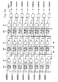
- This packet switching node 20 comprises four input ports 21, four queue selectors 22, four queue sets 23, four output arbitrators 24 and four output ports 25.
- Each of the queue sets 23 comprise four queues which are coupled between outputs of their repsective queue selectors 22 and the inputs of each of the four output arbitrators 24.
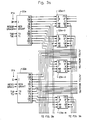
- Fig. 3 a detailed block diagram of the packet switching node 20 of Fig. 2 is shown.
- Fig. 3 is comprised of Figs. 3a and 3b, which should be placed adjacent to each other to obtain the complete drawing.
- This node comprises input ports 21a-d, queue selectors 22a-d, queue sets 23a-d comprised of four queues 23a-1 to 23a-4, etc., four output arbitrators 24a-d and four output ports 25a-d.
- a clock generator 26 is coupled to the various components of the node 20. Each of the components are shown illustrating the signal lines connected to other components of switching node 20.
- Each of the four queue selectors 22 is shown as an individual block.
- Each queue of a particular queue set 23 is shown as an individual block.
- Each output arbitrator 24 is shown as two blocks comprising data logic 24a-1 to 24d-1 and control logic 24a-2 to 24d-2.
- FIG. 4 Each of the components comprising the packet switching node 20 of Fig. 3 are illustrated in detail in Figs. 4 through 8. A detailed discussion of the design and construction of these circuits will be dispensed with due to the straightforward design thereof. However, components whose design or operation is not well known will be described in detail. It is to be understood that these circuits are illustrative of but a few of the many possible logic circuits which implement the desired logic equations and decision-making algorithms embodied therein.
- Fig. 4 illustrates the design of a clock generator 26 for use in the packet switching node 20 of Fig. 3.
- the various input and output lines and signal identifications delineated in Fig. 4 correspond to signal lines identified in Fig. 3 described above and Figs. 5 through 8.
- the clock generator 26 is comprised of a divide-by-three counter 34 coupled to a decoder 32 and a reset flip-flop 31.
- the divide-by-three counter 34 is comprised of flip-flops 30, feedback gates 33 and buffers 35.
- the counter 34 generates clock signal outputs in the sequence 00, 01, 10, 00 .... These signals are converted into three clock phases, REQO, GRAO and XFER ⁇ by the decoder 32.
- the reset flip-flop 31 synchronizes the MASTER RESET signal with the clock signal to produce a synchronous RESET signal for the system.
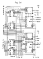
- Fig. 5 is comprised of Figs. 5a and 5b, which should be joined to form the complete drawing, as illustrated with reference to Fig. 3 above.
- Fig. 5 illustrates the design of queue selector logic associated with each of the queue selectors 22 of Fig. 3. Again, each of the signal lines is identified and corresponds to the signal lines of the other components illustrated in Figs. 4 through 8.
- the queue selector logic comprises a tag decoder 40, grant generation logic 41 and an eight-input, one-to-four demultiplexer 42. In operation, this logic receives a request signal, two tag bits and eight data bits at the beginning of the REQO clock which comprises the request phase.
- the tag signals are decoded by the tag decoder 40 which selects one of the four queues using the one-to-four demultiplexer 42. If the selected queue is not full, indicated by FULLi from the i-th queue, then the one-to-four demultiplexer 42 is enabled and a GRANT signal is produced by the grant generation logic 41. If the selected queue is full, then no GRANT signal is given.
- Fig. 6 is comprised of Figs. 6a and 6b and should be joined in a manner similar to Fig. 3 in order to obtain the complete drawing.
- Fig. 6 illustrates the design of each queue shown in Fig. 3.
- Three data packets may be stored in storage registers 50a-c.
- the remainder of the logic controls the operation of the queue.
- This logic is comprised of a back pointer 52 coupled to a write decoder 53, and a front pointer 54 coupled to a read decoder 55. These components are coupled to an eight-input multiplexer 51, a status counter 56 which is coupled to a status decoder 57, counter enable logic 58, and timing flip-flops 59.
- Each queue for example queue 23a-1, operates as follows. Data packets are received at the back of the queue from the one-to-four demultiplexer 42 in the queue selector 22. If the queue 23a-1 is not full, as indicated by the status decoder 57, a data packet will be written into one of the registers 50 pointed to by the back pointer 52. The selected register 50 is enabled by the write decoder 53 during the transfer phase signaled by the XFER0 clock. Upon receipt of the next request, the back pointer is incremented if enabled by the timing flip-flop 59b which controls the increment operation. A write clock pulse sent to the write decoder 53 is terminated by the timing flip-flop 59a. It is to be pointed out that this timing flip-flop is only needed if the registers 50 are level triggered. It may be removed from the circuitry if they are edge triggered.
- the status counter 56 is incremented. Each time a data packet is transmitted, the status counter 56 is decremented. The operation performed is determined by the counter enable logic 58 which examines an increment back INCBACK signal from the queue selector 22 and the increment front INCFRONT signal from the output arbitrator 24. If the status counter 56 is 00, then the status decode logic 57 indicates the empty state and if the status counter 56 is 11, then the status decoder logic 57 indicates the full state.
- a signal is sent to the output arbitrator 24 which requests to output a data packet from the front of the queue to the corresponding output port 25. If the output arbitrator 24 selects this queue and the data packet is transmitted, then the INCFRONT signal will be activated and during the transfer phase the front pointer 54 will be incremented.
- the read decoder 55 decodes the signals from the front pointer 54 and enables the output from the selected register 50 to appear at the front of the queue using the 8- input multiplexer 51.
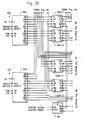
- the output arbitrator control logic 24a-2 is shown in Fig. 7.
- Fig. 7 is comprised of Figs. 7a and 7b, which should be joined to obtain the completed drawing as indicated with reference to Fig. 3 above.
- Each of the circuits comprising the output arbitrator control logic 24a-c is comprised of arbitration logic 60, incfront generation logic 61, priority counter 62 and priority counter enable logic 63.
- the arbitration logic 60 can receive requests from a total of four queues by way of "not empty" signals to transmit a packet from the corresponding output port 25. One queue is selected according to the priority indicated by the priority counter 62 and a request out signal is output therefrom.
- the priority counter 62 is incremented and thus the priority changes if a signal is received from the priority counter enable logic 63. Such a signal is produced only if the data packet with highest priority is transmitted, which is indicated by the receipt of a grant in signal.
- the incfront generation logic 61 sends a signal to increment the front pointer of the selected queue if a grant in signal has been received.
- the output of the arbitration logic 60 controls the output arbitrator data logic 24a-1.
- the output arbitrator data logic 24a-1 is shown in Fig. 8 and is comprised of an eight-input four-to-one multiplexer which connects the selected queue to this output port 25.
- Fig. 8 is comprised of Figs. 8a and 8b and should be joined as indicated hereinabove with reference to Fig. 3 to obtain the completed drawing.
- Fig. 9 shows the detailed logic diagram of a modulo three counter used to implement the back pointer 52 and front pointer 54 in the queue 23 shown in Fig. 6.
- Fig. 10 shows the detailed logic diagram of the modulo four up/down counter 56 in the queue 23 shown in Fig. 6.
- Fig. 11 shows the detailed logic diagram of a two-to-three demultiplexer used to implement the write decode logic 53 and read decode logic 55 in the queue 23 in Fig. 6.
- Fig. 12 shows the detailed logic of a modulo four up-counter used to implement the priority counter 62 in the output arbitrator control logic 24a-2 shown in Fig. 7.
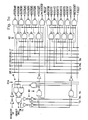
- Figs. 13 and 14 show timing diagrams for the packet switching node of Fig. 3.
- Fig. 13 shows the worst case timing analysis, when the queue is empty, and it accepts and transmits one data packet.
- Fig. 14 shows the worst case timing analysis when the queue has two data packets stored therein and it accepts one data packet, becomes full, and then transfers one data packet.
- the dashed lines indicate the soonest time that the particular signal could appear.
- the arrows are routed to events that occur in response to the happening of the event from which the arrows eminate.
- the present invention also contemplates a method of processing applied data packets containing routing tag signals indicative of the output port destinations to which the data packets are to be applied.
- the method processes the data packets in order to route them to the appropriate output ports.
- the method comprising the steps of sorting the data packets in accordance with the routing tag signals contained therein.
- the sorting function is performed by the queue selectors.
- the second step involves storing the data packets in predetermined queues associated with respective ones of each of the output ports in accordance with the routing tag signals.
- the next step comprises arbitrating, or selecting, among data packets that have been stored in the queues that contend for the same output port.
- the arbitration process is performed by the output arbitrators.
- the final step involves applying, or routing, the selected data packet to the output port identified in the routing tag signal. This final step is also performed by the output arbitrators.
- the packet switching node eliminates the problem of contention between data packets arriving at an input port of the node whose destinations are different output ports.
- the packet switching node sorts applied data packets according to output port destination utilizing a plurality of queues coupled to each input port in order to reduce contention.
- the present invention also provides for packet switching node which has improved performance and higher throughput.
- the present invention also provides for a data processing method for use in packet switching nodes which operates to reduce contention and increase system throughput.
- interconnection networks employing the present invention may be used to connect telephone systems that communicate both data and voice information by way of data packets.
Abstract
Claims (2)
Applications Claiming Priority (2)
| Application Number | Priority Date | Filing Date | Title |
|---|---|---|---|
| US06/662,474 US4623996A (en) | 1984-10-18 | 1984-10-18 | Packet switched multiple queue NXM switch node and processing method |
| US662474 | 1984-10-18 |
Publications (2)
| Publication Number | Publication Date |
|---|---|
| EP0200780A1 EP0200780A1 (fr) | 1986-11-12 |
| EP0200780B1 true EP0200780B1 (fr) | 1989-10-18 |
Family
ID=24657876
Family Applications (1)
| Application Number | Title | Priority Date | Filing Date |
|---|---|---|---|
| EP85905948A Expired EP0200780B1 (fr) | 1984-10-18 | 1985-09-26 | PROCEDE DE TRAITEMENT ET NOEUD DE COMMUTATION NxM A FILES D'ATTENTE MULTIPLES ET A PAQUETS COMMUTES |
Country Status (7)
| Country | Link |
|---|---|
| US (1) | US4623996A (fr) |
| EP (1) | EP0200780B1 (fr) |
| KR (2) | KR900006793B1 (fr) |
| DE (1) | DE3573871D1 (fr) |
| IL (1) | IL76534A0 (fr) |
| SG (1) | SG74589G (fr) |
| WO (1) | WO1986002510A1 (fr) |
Families Citing this family (86)
| Publication number | Priority date | Publication date | Assignee | Title |
|---|---|---|---|---|
| US4920534A (en) * | 1986-02-28 | 1990-04-24 | At&T Bell Laboratories | System for controllably eliminating bits from packet information field based on indicator in header and amount of data in packet buffer |
| NL8601712A (nl) * | 1986-07-01 | 1988-02-01 | Koninkl Philips Electronics Nv | Communicatienetwerk, in het bijzonder een telefoonnetwerk en datacommunicatienetwerk dat is samengesteld uit een verzameling van knooppuntseenheden, waarbij specifieke faciliteiten binnen naar keuze vastgestelde domeinen, volledig geintegreerd kunnen worden geboden. |
| US4754451A (en) * | 1986-08-06 | 1988-06-28 | American Telephone And Telegraph Company, At&T Bell Laboratories | N-by-N "knockout" switch for a high-performance packet switching system with variable length packets |
| US4760570A (en) * | 1986-08-06 | 1988-07-26 | American Telephone & Telegraph Company, At&T Bell Laboratories | N-by-N "knockout" switch for a high-performance packet switching system |
| EP0257168B1 (fr) * | 1986-08-27 | 1992-06-03 | International Business Machines Corporation | Appareil de transport pseudo-synchrone dans un réseau de communication |
| US4821259A (en) * | 1986-09-05 | 1989-04-11 | American Telephone And Telegraph Company, At&T Bell Laboratories | Control information communication arrangement for a distributed control switching system |
| US4780870A (en) * | 1986-09-05 | 1988-10-25 | American Telephone And Telegraph Company, At&T Bell Laboratories | Packet switch |
| EP0259117B1 (fr) * | 1986-09-05 | 1994-01-26 | AT&T Corp. | Système de commutation à paquets distribué |
| KR910002325B1 (ko) * | 1987-01-12 | 1991-04-11 | 후지쓰 가부시기가이샤 | 데이타 교환용 데이타 전송 버퍼회로 |
| US4887076A (en) * | 1987-10-16 | 1989-12-12 | Digital Equipment Corporation | Computer interconnect coupler for clusters of data processing devices |
| EP0312628B1 (fr) * | 1987-10-20 | 1993-12-29 | International Business Machines Corporation | Dispositif modulaire de commutation à grande vitesse pour le trafic en mode circuit et paquet |
| DE3738177A1 (de) * | 1987-11-10 | 1989-05-18 | Siemens Ag | Vermittlungsknoten fuer die vermittlung von in datenpaketen uebertragenen datensignalen |
| DE3878647D1 (de) * | 1987-11-11 | 1993-04-01 | Siemens Ag | Vermittlungsknoten fuer die vermittlung von in datenpaketen uebertragenen datensignalen. |
| AU625592B2 (en) * | 1988-03-26 | 1992-07-16 | Alcatel N.V. | Communication switching element |
| US5268896A (en) * | 1988-03-26 | 1993-12-07 | Alcatel N.V. | Communication switching element |
| SE462361B (sv) * | 1988-03-30 | 1990-06-11 | Ellemtel Utvecklings Ab | Paketdatavaeljare |
| US4872159A (en) * | 1988-03-31 | 1989-10-03 | American Telephone And Telegraph Company At&T Bell Laboratories | Packet network architecture for providing rapid response time |
| GB8810094D0 (en) * | 1988-04-28 | 1988-06-02 | Plessey Co Plc | Asychronous time division network |
| DE3823878A1 (de) * | 1988-07-14 | 1990-01-18 | Philips Patentverwaltung | Koppelfeld fuer ein vermittlungssystem |
| GB8821409D0 (en) * | 1988-09-13 | 1988-10-12 | Int Computers Ltd | Data processing system |
| DE3833490A1 (de) * | 1988-10-01 | 1990-04-05 | Philips Patentverwaltung | Koppelfeld fuer ein vermittlungssystem |
| US5210744A (en) * | 1989-06-28 | 1993-05-11 | Mitsubishi Denki Kabushiki Kaisha | Cell exchange apparatus |
| US4955016A (en) * | 1989-08-29 | 1990-09-04 | At&T Bell Laboratories | Interconnect fabric providing connectivity between an input and arbitrary output(s) of a group of outlets |
| US4955017A (en) * | 1989-08-29 | 1990-09-04 | At&T Bell Laboratories | Growable packet switch architecture |
| JPH03182140A (ja) * | 1989-12-11 | 1991-08-08 | Mitsubishi Electric Corp | 共通バッファ形交換装置 |
| US5247613A (en) * | 1990-05-08 | 1993-09-21 | Thinking Machines Corporation | Massively parallel processor including transpose arrangement for serially transmitting bits of data words stored in parallel |
| CA2043505A1 (fr) * | 1990-06-06 | 1991-12-07 | Steven K. Heller | Processeur massivement parallele comportant un systeme de transmission de messages a file d'attente |
| US5191578A (en) * | 1990-06-14 | 1993-03-02 | Bell Communications Research, Inc. | Packet parallel interconnection network |
| US5265257A (en) * | 1990-06-22 | 1993-11-23 | Digital Equipment Corporation | Fast arbiter having easy scaling for large numbers of requesters, large numbers of resource types with multiple instances of each type, and selectable queuing disciplines |
| US5265229A (en) * | 1990-07-02 | 1993-11-23 | Digital Equipment Corporation | Single load, multiple issue queue with error recovery capability |
| US5231633A (en) * | 1990-07-11 | 1993-07-27 | Codex Corporation | Method for prioritizing, selectively discarding, and multiplexing differing traffic type fast packets |
| US5172371A (en) * | 1990-08-09 | 1992-12-15 | At&T Bell Laboratories | Growable switch |
| CA2048198C (fr) | 1990-08-09 | 1996-06-04 | Kai Y. Eng | Commutation modulaire |
| US5166930A (en) * | 1990-12-17 | 1992-11-24 | At&T Bell Laboratories | Data channel scheduling discipline arrangement and method |
| US5144293A (en) * | 1990-12-18 | 1992-09-01 | International Business Machines Corporation | Serial link communication system with cascaded switches |
| US5404461A (en) * | 1991-03-29 | 1995-04-04 | International Business Machines Corp. | Broadcast/switching apparatus for executing broadcast/multi-cast transfers over unbuffered asynchronous switching networks |
| US5250943A (en) * | 1991-03-29 | 1993-10-05 | International Business Machines Corporation | GVT-NET--A Global Virtual Time Calculation Apparatus for Multi-Stage Networks |
| US5365228A (en) * | 1991-03-29 | 1994-11-15 | International Business Machines Corporation | SYNC-NET- a barrier synchronization apparatus for multi-stage networks |
| JP2947628B2 (ja) * | 1991-03-11 | 1999-09-13 | 富士通株式会社 | スイッチ制御装置 |
| US5825773A (en) * | 1991-03-20 | 1998-10-20 | Hitachi, Ltd. | Switching system for transferring broadcast packet held in broadcast buffer received from input port to output ports according to the state of each output port |
| GB2254980B (en) * | 1991-04-16 | 1995-03-08 | Roke Manor Research | Improvements in or relating to multicast server apparatus |
| US5321813A (en) * | 1991-05-01 | 1994-06-14 | Teradata Corporation | Reconfigurable, fault tolerant, multistage interconnect network and protocol |
| US5268900A (en) * | 1991-07-05 | 1993-12-07 | Codex Corporation | Device and method for implementing queueing disciplines at high speeds |
| JP3679813B2 (ja) * | 1991-07-22 | 2005-08-03 | 株式会社日立製作所 | 並列計算機 |
| JP2671699B2 (ja) * | 1991-11-15 | 1997-10-29 | 三菱電機株式会社 | セル交換装置 |
| US5398235A (en) * | 1991-11-15 | 1995-03-14 | Mitsubishi Denki Kabushiki Kaisha | Cell exchanging apparatus |
| US5243699A (en) * | 1991-12-06 | 1993-09-07 | Maspar Computer Corporation | Input/output system for parallel processing arrays |
| GB2272820B (en) * | 1992-11-14 | 1996-08-07 | Roke Manor Research | Improvements in or relating to asynchronous transfer mode communication systems |
| EP0612171B1 (fr) * | 1993-02-15 | 2001-11-28 | Mitsubishi Denki Kabushiki Kaisha | Dispositif de file d'attente de données et commutateur de cellules ATM par décalage et recherche |
| SE515148C2 (sv) * | 1993-06-23 | 2001-06-18 | Ericsson Telefon Ab L M | Styrning av cellväljare |
| US5613067A (en) * | 1993-12-30 | 1997-03-18 | International Business Machines Corporation | Method and apparatus for assuring that multiple messages in a multi-node network are assured fair access to an outgoing data stream |
| US5495426A (en) * | 1994-01-26 | 1996-02-27 | Waclawsky; John G. | Inband directed routing for load balancing and load distribution in a data communication network |
| EP0669736A3 (fr) * | 1994-01-26 | 1997-01-08 | Ibm | Routage dynamique en temps réel dans un réseau de données. |
| GB2288095A (en) * | 1994-03-23 | 1995-10-04 | Roke Manor Research | Improvements in or relating to asynchronous transfer mode (ATM) systems |
| GB2288096B (en) * | 1994-03-23 | 1999-04-28 | Roke Manor Research | Apparatus and method of processing bandwidth requirements in an ATM switch |
| GB2288947B (en) * | 1994-04-20 | 1999-01-06 | Roke Manor Research | Improvements in or relating to ATM communication systems |
| SE504985C2 (sv) * | 1995-05-09 | 1997-06-09 | Ericsson Telefon Ab L M | ATM-växelkärna |
| US6141346A (en) * | 1995-07-19 | 2000-10-31 | Fujitsu Network Communications, Inc. | Point-to-multipoint transmission using subqueues |
| US6185222B1 (en) | 1995-09-28 | 2001-02-06 | Cisco Technology, Inc. | Asymmetric switch architecture for use in a network switch node |
| FR2741763B1 (fr) * | 1995-11-23 | 1998-01-23 | Jean Louis Simon | Systeme de regulation de trains d'information pour commutateur paquet |
| US5790545A (en) * | 1996-03-14 | 1998-08-04 | Motorola Inc. | Efficient output-request packet switch and method |
| US5742597A (en) * | 1996-03-14 | 1998-04-21 | Motorola, Inc. | Method and device for multipoint switching and arbitration in output-request packet switch |
| US5878227A (en) * | 1996-07-01 | 1999-03-02 | Sun Microsystems, Inc. | System for performing deadlock free message transfer in cyclic multi-hop digital computer network using a number of buffers based on predetermined diameter |
| US6049546A (en) * | 1996-10-15 | 2000-04-11 | At&T Corporation | System and method for performing switching in multipoint-to-multipoint multicasting |
| US6115387A (en) * | 1997-02-14 | 2000-09-05 | Advanced Micro Devices, Inc. | Method and apparatus for controlling initiation of transmission of data as a function of received data |
| KR100327986B1 (ko) * | 1997-12-20 | 2002-08-08 | 주식회사 하이닉스반도체 | 웨이트-플레그를이용한딜레이트래픽프레임의선택방법 |
| DE69940571D1 (de) * | 1998-12-03 | 2009-04-23 | Agency Ind Science Techn | Kommunikationsverfahren und -system |
| US6574232B1 (en) * | 1999-05-26 | 2003-06-03 | 3Com Corporation | Crossbar switch utilizing broadcast buffer and associated broadcast buffer management unit |
| US6418526B1 (en) | 1999-11-15 | 2002-07-09 | Ncr Corporation | Method and apparatus for synchronizing nodes in massively parallel systems |
| US6412002B1 (en) | 1999-11-15 | 2002-06-25 | Ncr Corporation | Method and apparatus for selecting nodes in configuring massively parallel systems |
| US6745240B1 (en) | 1999-11-15 | 2004-06-01 | Ncr Corporation | Method and apparatus for configuring massively parallel systems |
| US6519697B1 (en) | 1999-11-15 | 2003-02-11 | Ncr Corporation | Method and apparatus for coordinating the configuration of massively parallel systems |
| US7106728B1 (en) | 2000-05-01 | 2006-09-12 | Industrial Technology Research Institute | Switching by multistage interconnection of concentrators |
| US6591285B1 (en) * | 2000-06-16 | 2003-07-08 | Shuo-Yen Robert Li | Running-sum adder networks determined by recursive construction of multi-stage networks |
| US6807186B2 (en) * | 2001-04-27 | 2004-10-19 | Lsi Logic Corporation | Architectures for a single-stage grooming switch |
| US7006497B2 (en) * | 2001-06-04 | 2006-02-28 | Calix Networks, Inc. | Traffic merging system |
| US7035294B2 (en) * | 2001-06-04 | 2006-04-25 | Calix Networks, Inc. | Backplane bus |
| US7068672B1 (en) * | 2001-06-04 | 2006-06-27 | Calix Networks, Inc. | Asynchronous receive and transmit packet crosspoint |
| US7103059B2 (en) * | 2001-06-15 | 2006-09-05 | Industrial Technology Research Institute | Scalable 2-stage interconnections |
| US7609695B2 (en) * | 2001-06-15 | 2009-10-27 | Industrial Technology Research Institute | Optimizing switching element for minimal latency |
| US6999453B1 (en) | 2001-07-09 | 2006-02-14 | 3Com Corporation | Distributed switch fabric arbitration |
| US7269158B2 (en) * | 2002-03-06 | 2007-09-11 | International Business Machines Corporation | Method of operating a crossbar switch |
| US7151777B2 (en) * | 2002-04-04 | 2006-12-19 | Fujitsu Limited | Crosspoint switch having multicast functionality |
| US7512148B2 (en) * | 2003-12-09 | 2009-03-31 | Texas Instruments Incorporated | Weighted round-robin arbitrator |
| GB2495543A (en) * | 2011-10-14 | 2013-04-17 | St Microelectronics Res & Dev | An arrangement for routing requests |
| US20140050221A1 (en) * | 2012-08-16 | 2014-02-20 | Stmicroelectronics, Inc. | Interconnect arrangement |
Family Cites Families (4)
| Publication number | Priority date | Publication date | Assignee | Title |
|---|---|---|---|---|
| FR2447652A1 (fr) * | 1979-01-24 | 1980-08-22 | Materiel Telephonique | Operateur pour reseau de commutation de donnees numeriques par paquets |
| FR2458196A1 (fr) * | 1979-06-01 | 1980-12-26 | Materiel Telephonique | Niveau de commutation d'un operateur pour reseau de commutation de donnees numeriques par paquets |
| US4482996A (en) * | 1982-09-02 | 1984-11-13 | Burroughs Corporation | Five port module as a node in an asynchronous speed independent network of concurrent processors |
| FR2549673B1 (fr) * | 1983-07-19 | 1989-06-30 | Thomson Csf Mat Tel | Commutateur elementaire pour autocommutateur utilisant une technique de multiplexage asynchrone |
-
1984
- 1984-10-18 KR KR1019860700371A patent/KR900006793B1/ko active
- 1984-10-18 US US06/662,474 patent/US4623996A/en not_active Expired - Lifetime
-
1985
- 1985-09-26 KR KR1019860700371A patent/KR880700568A/ko not_active IP Right Cessation
- 1985-09-26 EP EP85905948A patent/EP0200780B1/fr not_active Expired
- 1985-09-26 WO PCT/US1985/001838 patent/WO1986002510A1/fr active IP Right Grant
- 1985-09-26 DE DE8585905948T patent/DE3573871D1/de not_active Expired
- 1985-09-29 IL IL76534A patent/IL76534A0/xx not_active IP Right Cessation
-
1989
- 1989-11-16 SG SG745/89A patent/SG74589G/en unknown
Also Published As
| Publication number | Publication date |
|---|---|
| KR880700568A (ko) | 1988-03-15 |
| SG74589G (en) | 1990-04-20 |
| US4623996A (en) | 1986-11-18 |
| WO1986002510A1 (fr) | 1986-04-24 |
| DE3573871D1 (en) | 1989-11-23 |
| IL76534A0 (en) | 1986-01-31 |
| EP0200780A1 (fr) | 1986-11-12 |
| KR900006793B1 (ko) | 1990-09-21 |
Similar Documents
| Publication | Publication Date | Title |
|---|---|---|
| EP0200780B1 (fr) | PROCEDE DE TRAITEMENT ET NOEUD DE COMMUTATION NxM A FILES D'ATTENTE MULTIPLES ET A PAQUETS COMMUTES | |
| EP0198010B1 (fr) | PROCEDE DE TRAITEMENT ET NOEUD DE COMMUNICATION NxM A MEMOIRE MULTIPORTE A COMMUTATION PAR PAQUETS | |
| US6314487B1 (en) | Adaptive routing controller of a crossbar core module used in a crossbar routing switch | |
| Tamir et al. | Dynamically-allocated multi-queue buffers for VLSI communication switches | |
| EP0197103B1 (fr) | Equilibrage de la charge pour noeuds de commutation par paquets | |
| Tamir et al. | High-performance multi-queue buffers for VLSI communications switches | |
| EP0018755B1 (fr) | Réseaux de communication digitale, utilisant des commutateurs indépendants de la vitesse | |
| US7940666B2 (en) | Communication node architecture in a globally asynchronous network on chip system | |
| CA1263729A (fr) | Reseau en delta de commutateur d'interconnexion | |
| EP0405208B1 (fr) | Réseau à plusieurs étages avec commande répartie | |
| EP0369146A2 (fr) | Réseau hiérarchique multivoie | |
| KR19990087752A (ko) | 효율적인 출력 요구 패킷 스위치와 방법 | |
| JP3206126B2 (ja) | 分散クロスバー・スイッチ・アーキテクチャにおけるスイッチング・アレイ | |
| Konstantinidou | Deterministic and chaotic adaptive routing in multicomputers | |
| Lee | A virtual bus architecture for dynamic parallel processing | |
| Lee | A variable round-robin arbiter for high speed buses and statistical multiplexers | |
| Arango et al. | Staged circuit switching | |
| RU2115162C1 (ru) | Сеть для маршрутизации сообщений | |
| JP3031591B2 (ja) | アクセス調停方式 | |
| Youn et al. | On multistage interconnection networks with small clock cycles | |
| JPH0638608B2 (ja) | パケット・スイッチング・多重キュ−n×mスイッチ・ノ−ド及び処理方法 | |
| JP3112208B2 (ja) | マトリクス網回路 | |
| Lay | High-performance communication in parallel computers | |
| Ciminiera et al. | Interconnection networks for MIMD machines | |
| Kiamilev et al. | Modular architecture for smart pixel switching networks |
Legal Events
| Date | Code | Title | Description |
|---|---|---|---|
| PUAI | Public reference made under article 153(3) epc to a published international application that has entered the european phase |
Free format text: ORIGINAL CODE: 0009012 |
|
| 17P | Request for examination filed |
Effective date: 19860612 |
|
| AK | Designated contracting states |
Kind code of ref document: A1 Designated state(s): DE FR GB IT NL |
|
| 17Q | First examination report despatched |
Effective date: 19880413 |
|
| RAP1 | Party data changed (applicant data changed or rights of an application transferred) |
Owner name: HUGHES AIRCRAFT COMPANY |
|
| GRAA | (expected) grant |
Free format text: ORIGINAL CODE: 0009210 |
|
| AK | Designated contracting states |
Kind code of ref document: B1 Designated state(s): DE FR GB IT NL |
|
| REF | Corresponds to: |
Ref document number: 3573871 Country of ref document: DE Date of ref document: 19891123 |
|
| ET | Fr: translation filed | ||
| ITF | It: translation for a ep patent filed |
Owner name: SOCIETA' ITALIANA BREVETTI S.P.A. |
|
| PLBE | No opposition filed within time limit |
Free format text: ORIGINAL CODE: 0009261 |
|
| STAA | Information on the status of an ep patent application or granted ep patent |
Free format text: STATUS: NO OPPOSITION FILED WITHIN TIME LIMIT |
|
| 26N | No opposition filed | ||
| ITTA | It: last paid annual fee | ||
| PGFP | Annual fee paid to national office [announced via postgrant information from national office to epo] |
Ref country code: FR Payment date: 19940808 Year of fee payment: 10 |
|
| PGFP | Annual fee paid to national office [announced via postgrant information from national office to epo] |
Ref country code: GB Payment date: 19940815 Year of fee payment: 10 |
|
| PGFP | Annual fee paid to national office [announced via postgrant information from national office to epo] |
Ref country code: DE Payment date: 19940824 Year of fee payment: 10 |
|
| PGFP | Annual fee paid to national office [announced via postgrant information from national office to epo] |
Ref country code: NL Payment date: 19940930 Year of fee payment: 10 |
|
| PG25 | Lapsed in a contracting state [announced via postgrant information from national office to epo] |
Ref country code: GB Effective date: 19950926 |
|
| PG25 | Lapsed in a contracting state [announced via postgrant information from national office to epo] |
Ref country code: NL Effective date: 19960401 |
|
| GBPC | Gb: european patent ceased through non-payment of renewal fee |
Effective date: 19950926 |
|
| PG25 | Lapsed in a contracting state [announced via postgrant information from national office to epo] |
Ref country code: FR Effective date: 19960531 |
|
| PG25 | Lapsed in a contracting state [announced via postgrant information from national office to epo] |
Ref country code: DE Effective date: 19960601 |
|
| NLV4 | Nl: lapsed or anulled due to non-payment of the annual fee |
Effective date: 19960401 |
|
| REG | Reference to a national code |
Ref country code: FR Ref legal event code: ST |