EP0200602A1 - Three-dimensional activated liquid-crystal matrix display device, and process for operating it - Google Patents
Three-dimensional activated liquid-crystal matrix display device, and process for operating it Download PDFInfo
- Publication number
- EP0200602A1 EP0200602A1 EP86400690A EP86400690A EP0200602A1 EP 0200602 A1 EP0200602 A1 EP 0200602A1 EP 86400690 A EP86400690 A EP 86400690A EP 86400690 A EP86400690 A EP 86400690A EP 0200602 A1 EP0200602 A1 EP 0200602A1
- Authority
- EP
- European Patent Office
- Prior art keywords
- column
- small
- connections
- line
- packet
- Prior art date
- Legal status (The legal status is an assumption and is not a legal conclusion. Google has not performed a legal analysis and makes no representation as to the accuracy of the status listed.)
- Granted
Links
- 239000004973 liquid crystal related substance Substances 0.000 title claims abstract description 24
- 239000011159 matrix material Substances 0.000 title claims abstract description 13
- 238000000034 method Methods 0.000 title claims abstract description 12
- 230000000737 periodic effect Effects 0.000 claims description 7
- 239000010409 thin film Substances 0.000 claims description 5
- 230000000903 blocking effect Effects 0.000 claims description 4
- 238000010586 diagram Methods 0.000 description 2
- 230000005284 excitation Effects 0.000 description 2
- 230000003287 optical effect Effects 0.000 description 2
- 230000008033 biological extinction Effects 0.000 description 1
- 230000007423 decrease Effects 0.000 description 1
- 230000005684 electric field Effects 0.000 description 1
- 238000012423 maintenance Methods 0.000 description 1
- 230000005693 optoelectronics Effects 0.000 description 1
- 238000007789 sealing Methods 0.000 description 1
Images

Classifications
-
- G—PHYSICS
- G02—OPTICS
- G02F—OPTICAL DEVICES OR ARRANGEMENTS FOR THE CONTROL OF LIGHT BY MODIFICATION OF THE OPTICAL PROPERTIES OF THE MEDIA OF THE ELEMENTS INVOLVED THEREIN; NON-LINEAR OPTICS; FREQUENCY-CHANGING OF LIGHT; OPTICAL LOGIC ELEMENTS; OPTICAL ANALOGUE/DIGITAL CONVERTERS
- G02F1/00—Devices or arrangements for the control of the intensity, colour, phase, polarisation or direction of light arriving from an independent light source, e.g. switching, gating or modulating; Non-linear optics
- G02F1/01—Devices or arrangements for the control of the intensity, colour, phase, polarisation or direction of light arriving from an independent light source, e.g. switching, gating or modulating; Non-linear optics for the control of the intensity, phase, polarisation or colour
- G02F1/13—Devices or arrangements for the control of the intensity, colour, phase, polarisation or direction of light arriving from an independent light source, e.g. switching, gating or modulating; Non-linear optics for the control of the intensity, phase, polarisation or colour based on liquid crystals, e.g. single liquid crystal display cells
- G02F1/133—Constructional arrangements; Operation of liquid crystal cells; Circuit arrangements
- G02F1/136—Liquid crystal cells structurally associated with a semi-conducting layer or substrate, e.g. cells forming part of an integrated circuit
- G02F1/1362—Active matrix addressed cells
-
- G—PHYSICS
- G02—OPTICS
- G02F—OPTICAL DEVICES OR ARRANGEMENTS FOR THE CONTROL OF LIGHT BY MODIFICATION OF THE OPTICAL PROPERTIES OF THE MEDIA OF THE ELEMENTS INVOLVED THEREIN; NON-LINEAR OPTICS; FREQUENCY-CHANGING OF LIGHT; OPTICAL LOGIC ELEMENTS; OPTICAL ANALOGUE/DIGITAL CONVERTERS
- G02F1/00—Devices or arrangements for the control of the intensity, colour, phase, polarisation or direction of light arriving from an independent light source, e.g. switching, gating or modulating; Non-linear optics
- G02F1/01—Devices or arrangements for the control of the intensity, colour, phase, polarisation or direction of light arriving from an independent light source, e.g. switching, gating or modulating; Non-linear optics for the control of the intensity, phase, polarisation or colour
- G02F1/13—Devices or arrangements for the control of the intensity, colour, phase, polarisation or direction of light arriving from an independent light source, e.g. switching, gating or modulating; Non-linear optics for the control of the intensity, phase, polarisation or colour based on liquid crystals, e.g. single liquid crystal display cells
- G02F1/133—Constructional arrangements; Operation of liquid crystal cells; Circuit arrangements
- G02F1/1333—Constructional arrangements; Manufacturing methods
- G02F1/1343—Electrodes
- G02F1/134309—Electrodes characterised by their geometrical arrangement
- G02F1/134336—Matrix
Definitions
- the present invention relates to a liquid crystal matrix display device with three-dimensional control and its control method.
- the invention applies in particular in optoelectronics and mainly in the control of liquid crystal matrix display devices, used for example as converters of electrical information into optical information, for the processing of optical images in real time, and for analog display.
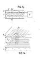
- FIG. 1a represents a matrix display device with liquid crystal with crossed bands according to the prior art
- FIG. 1b representing this device in exploded view.
- FIG. 1 a In FIG. 1 a are shown two insulating walls 1,3 facing one another, kept apart by a sealing joint 2 disposed around their edges and between which a layer of liquid crystal 4 is introduced.
- a first family of m lines of electrodes denoted L ;, parallel, with i integer such as 1 5 i 5 m, constituted by continuous conductive strips and on the internal face of l the other wall 3 is distributed a second family of q columns of electrodes, denoted C j , parallel, with j integer such as 1 ⁇ j ⁇ q, also constituted by conductive strips, the m lines and the q columns of electrodes being crossed.
- These m lines and q columns of electrodes are used to convey electrical signals, respectively line signals and column signals suitable for the excitation of the liquid crystal. These signals are produced in a known manner by a power source 6.
- FIG. 1 b representing this device in exploded view, we see the first family of m rows of electrodes, denoted L i and the second family of q columns of electrodes, denoted C j , distributed respectively on the walls 1 and 3.
- an area l ij of liquid crystal is defined by the overlap region of the row L i and of the column C j .
- Each zone l ij defines an elementary image point of the display device; the latter therefore comprises mxq image points distributed in a matrix.
- alternating electrical signals in phase or in phase opposition are applied to the m rows and q columns of electrodes, the amplitude of the row signals being slightly greater than that of the column signals.
- the resulting signal When the signal of line L i and the signal of column C j are in phase, the resulting signal is equal to the difference of the amplitudes in absolute value of the line signal and the column signal. The resulting signal is then lower than the threshold voltage V s of the liquid crystal, corresponding to the minimum voltage necessary to excite the liquid crystal. Also, in the overlap area i ij the liquid crystal not being excited, a black point is displayed. On the other hand, when the signal of the line L i and the signal of the column C j are in phase opposition, the resulting signal has an amplitude equal to the sum of the amplitudes in absolute value of the line signal and the column signal. The resulting signal creates an electric field in the overlap zone I ii which generally causes a collective orientation of molecules in this zone and therefore the display of white.
- each row and of each column is associated for example a switch such as a thin film transistor which transmits to the corresponding zone I ij , the signal resulting from the line signal applied to the line L i and from the column signal applied to column C j .
- a switch such as a thin film transistor which transmits to the corresponding zone I ij , the signal resulting from the line signal applied to the line L i and from the column signal applied to column C j .
- the invention aims to remedy these drawbacks by producing in particular a display device comprising a number of connections and transistors lower than those of the known devices of the prior art, without however reducing the number of elementary image points.
- each small line is associated with a switch serving on the one hand to connect together the n small lines of an electrode line and to connect together the electrode lines in order to form s line connections and on the other hand to connect the s small lines of each line packet P k in order to form p first packet connections and in that each small column is associated with a switch serving firstly to connect them the r small columns of an electrode column and to connect the electrode columns to each other in order to form t column connections and on the other hand to connect the t small columns of each column packet T k to form p second packet connections, the line packet P k and the column packet T k being interconnected by the first and second corresponding packet connections.
- the electrode lines (La), (L 2s + 1-a ), - (L 2s + a ), (L 4s + 1-a ) and so on are interconnected to form s line connections and the electrode columns (C b ), (C 2t + 1-b ), (C 2t + b ), (C 4t + 1-b ) and so on are connected between them to form t column connections, a and b being integers such as 1 ⁇ a ⁇ m and 1 ⁇ b ⁇ q.
- the electrode lines (La), - (La + s), (L a + 2s ), (La + 3s) and so on are connected together to form s line connections and the electrode columns (C b ), (C b + t ), (C b + 2t ), (C b + 3t ) and so on are connected together to form t column connections, a and b being integers such as 1 ⁇ a ⁇ m and 1 ⁇ b ⁇ q.
- the switches are thin film transistors.
- the line signals and the column signals are either in phase or in phase opposition.
- the packet signals select either the on state or the blocking state of said transistors associated with packet connections.
- the electrical signals applied are rectangular signals.
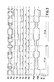
- FIG. 2 represents an example of a matrix display device according to the invention.
- the device of the invention comprises, like those of the prior art (FIGS. 1) two walls 1, 3 facing each other, covered respectively by a first family of m lines of electrodes, denoted La, and by a second fa thousand of q columns of electrodes denoted C b , a and b being thirds such as 1 ⁇ a 5 m and 1 ⁇ b ⁇ q.
- a layer of liquid crystal 4 is interposed between the two families of electrodes.
- the first family of m rows of electrodes is made up of discontinuous conductive strips each formed by n small stripes lines 5,7, 9.
- Each row packet, denoted P k therefore consists of s small rows, denoted l i
- each column packet, denoted T k consists of t small columns, denoted c j , with i, j and k being integers such as 1 ⁇ i ⁇ s, 1 ⁇ j ⁇ t and 1 ⁇ k ⁇ p.
- an image point I ijk is defined by the overlap region between a small row I i of a row packet P k and a small column c j of the corresponding column packet T k .
- each small line I i and each small column c j is associated respectively with a switch 15, 17, such as a thin film transistor, connected to each small line I i and to each small column c j by the drain - (or the source) of it.
- the transistors 15 associated with the small lines, denoted I i thus make it possible, via their source (or their drain), to connect together the n small lines constituting a line of electrodes and to connect the lines together (La), (La + s), (L a + 2s ) etc ... or the lines (La), (L 2s + 1-a ), (L 2 s + a), (L 4s + 1 -a ), etc ... as in the example in the figure, to form s line connections, denoted X i .
- the line L is connected to the line L, o , the line L2 to the line L 9 , etc. thus forming 5 line connections.
- the transistors 15 also make it possible, via their grid, to connect the small lines of each line packet P kP to form p first packet connections, denoted Z k , p being equal to 6 in the example of the figure.
- the transistors 17 associated with the small columns make it possible, via their source (or their drain), to connect the r small columns forming an electrode column to one another and to connect between them the columns (C b ), C b + t ), (C b + 2t ); etc ... or the columns (C b ), (C 2t + 1-b ), (C 2t + b ), (C 4t + 1-b ), etc ... as in the example in the figure , to form t column connections, noted Y j .
- the transistors 17 also make it possible, via their grid, to connect the t small columns of each column packet Tk to one another. to form p second packet connections, denoted Z k .
- the row packet P k and the column packet T k are interconnected by the first and second corresponding packet connections to form p packet connections, denoted Z k .
- Each overlap zone between the small line strip I i of a packet P k and the small column strip c j of the corresponding packet T k defines an image point I ijk .
- the signal which is seen by this image point therefore results from the superposition of a signal applied to the corresponding line connection, X;, called line signal F i , of a signal applied to the corresponding column connection Y j , called column signal G j and a signal applied to the corresponding packet connection Z k , called the packet signal H k .
- the resulting signal at the image point I ijk will be noted R ijk .
- control of such a device is therefore done by the superposition of three different types of signals F i , G j , H k , this type of control is therefore called three-dimensional control.
- the line signal F i is received by all of the transistors 15 connected to each other by their source (or their drain) and associated with the corresponding small line bands I i .
- the column signal G j is received by all of the transistors 17 connected to each other by their source (or their drain) and associated with the corresponding small column bands c j .
- the packet signal H k allows to pass or not the line signal F i and the column signal G j on the line I i and the column c j respectively of the packet P k , T k , which makes it possible to differentiate the different small bands rows I i of the p packets rows P k and the different small column strips c j of the p column packets T k .
- the corresponding transistors 15, 17 of the packets P k , T k are selected at the same time, depending on the signal applied, they are either in the on state, in this case they allow the line signal F and the column signal to pass G j , respectively on the line I i of the packet P k and the column c j of the corresponding packet T k , ie at high impedance, in this case, they do not allow any signal to pass.
- mq stp image points using only (s + t ) .p transistors and s + t + p connections.
- the transistors used in this type of device are preferably thin film transistors.
- FIG. 3 represents the timing diagram of the various control signals of the display device of FIG. 2.
- column signals G and G2 applied to the column connections Y ,, Y2, the line signals F ,, F 2 , ..., F s applied to the different line connections X 1 , X 2 , ..., X s , the packet signals H ,, H 2 , ..., H 6 applied to the different packet connections Z 1 , Z2, ..., Z6 as well as two examples of resulting signals R 111 and R 121 at the corresponding image points I 111 and I 121 .
- the signals lines F ,, F 2 , ..., F 5 and columns G ,, G 2 , ..., G6 of the display device are signals in particular rectangular of period T. These signals have their polarity which is inverse to each half-period, noted T / 2, to protect the liquid crystal from direct currents and thus prolong its service life. The average of these signals is therefore zero in each period.
- the time T / 2 corresponds to the periodic refresh of the information in the liquid crystal and therefore to the maintenance of the excited points.
- the time T / 2 is generally of the order of 20 ms.
- the line signals F ,, F 2 , ..., F s are impulsive, they are non-zero during a line time noted T L , equal to T / (2.s), s representing the number of line connections of the device d 'display.
- T L a line time
- the s line times are thus distributed over each half-period T / 2, at each time T L corresponding to a single non-zero pulse of a line signal.
- the time T L is the time necessary for memorizing the signal.
- the duration of the various signals F ,, F 2 , ..., F s is therefore respectively T / 10, that is to say of the order of 4 ms.
- the column signal G j is applied continuously, it is either in phase with the line signal F i considered, in this case, the corresponding image point is black, or in phase opposition therewith and in this case, the point image is white, with i and j in the display device described, integers such as 1 ⁇ i ⁇ 5 and 1 ⁇ j ⁇ 6.
- the signals G, and G 2 relative to the column connections Y, and Y 2 are identical but of opposite polarity.
- the column Y, or Y2 connections are therefore sent either the column signal G ,, or the column signal G2.
- the packet signals H 1 , H 2 , ..., H 6 control both the state of the transistors associated with the small row bands, denoted I i , of a row packet P k and those associated with the small column bands c j of the corresponding column packet T k , with k an integer such that 1 ⁇ k ⁇ 6.
- the packet signals are rectangular impulse signals.
- the duration of these signals, noted T c is equal to T L / p, p representing the number of packet connections Z k and T L the line time; T c is therefore equal to T / (2.sp). This time T c corresponds to the charging time of a transistor.
- T c therefore has a duration of the order of 0.66 ms.
- time T c a packet connection Z k receives the pulse signal H k , the transistors 15 associated with the small row bands of the packet P k and the transistors 17 associated with the small column bands of the packet T k are in the on state.
- the packet signal H k is zero, the transistors 15, 17 of the corresponding packets P k and T k are in the high impedance state, c is to say blocking.
- the signal R 111 corresponding to the superposition of a line signal F, applied to the connection X, of a column signal G, applied to the connection Y, and of a signal packet H, applied to connection Z is zero at the start of a half-period T / 2 during a line time T L because of the signals F, and G, in phase during the on state of the transistors associated with the line 1, and in column c, selected by the packet signal Z,; this zero signal then persists throughout the duration of the time T L corresponding to the storage time; this results in the display of a black I 111 image point.
- the line signal F being zero for the rest of the time T / 2
- the signal R 111 will therefore be that of the column signal G, at the moment when the packet signal H will select the passing from the corresponding transistor this small column band c ,.
- the amplitude of the column signal being lower than the value of the threshold voltage of the liquid crystal, the display of black at point I 111 will persist over the rest of the time T / 2.
- the resulting signal R 121 has an amplitude equal to the sum of the amplitudes in absolute value of the line signal F, and of the column signal G2 the fact that these signals are in phase opposition during the on state of the transistors, associated with line 1, and with column c 2 selected by the packet signal H ,. This results in a point I 121 in white.
- the signal F being zero over the rest of the time T / 2
- the signal R 121 depends on the column signal G 2 applied to the connection Y when the transistor of the column c 2 is selected by the signal package H ,.
- the white display at point I 121 therefore persists for the rest of the time T / 2. The same is true for each T / 2 half-period.
- the display device described above with three-dimensional control, that is to say using three types of signals applied to three types of connections, makes it possible to have relationships between the number of displayed points (stp) and the number of connections (s + t + p) and between the number of displayed points (stp) and the number of transistors (s + t) .p used, greater than those of known devices.
Landscapes
- Physics & Mathematics (AREA)
- Nonlinear Science (AREA)
- Mathematical Physics (AREA)
- Chemical & Material Sciences (AREA)
- Crystallography & Structural Chemistry (AREA)
- General Physics & Mathematics (AREA)
- Optics & Photonics (AREA)
- Engineering & Computer Science (AREA)
- Microelectronics & Electronic Packaging (AREA)
- Geometry (AREA)
- Liquid Crystal (AREA)
- Liquid Crystal Display Device Control (AREA)
- Control Of Indicators Other Than Cathode Ray Tubes (AREA)
- Devices For Indicating Variable Information By Combining Individual Elements (AREA)
Abstract
L'invention concerne un dispositif d'affichage matriciel à cristal liquide à commande tridimensionnelle et son procédé de commande. Le dispositif comprend deux parois isolantes (1, 3) en regard, recouvertes respectivement d'une première famille de m lignes d'électrodes formées chacune de n petites bandes lignes (5, 7, 9) et d'une deuxième famille de q colonnes d'électrodes croisées par rapport à la première et formées de r petites bandes colonnes (11, 13), une couche de cristal liquide intercalée entre la première et la deuxième famille ; les petites lignes et les petites colonnes étant regroupées respectivement en p paquets lignes, notés Pk, de s petites lignes, notées li et en p paquets colonnes, notés Tk, de t petites colonnes, notées cj, avec p=n.r, s=m.n/p, t=q.r/p et i, j, k entiers tels que 1 <= i <= s, 1 <= j <= t et 1 <= k <= p, chaque petite ligne et petite colonne étant associée respectivement à un in terrupteur (15, 17) permettant d'interconnecter les petites lignes et d'interconnecter les petites colonnes pour former s connexions lignes, notées Xi, t connexions colonnes, notées Yj, et p connexions paquets, notées Zk. Application aux cellules d'affichage cristal liquide.The invention relates to a three-dimensional control liquid crystal matrix display device and its control method. The device comprises two insulating walls (1, 3) facing each other, covered respectively with a first family of m rows of electrodes each formed by n small strip strips (5, 7, 9) and a second family of q columns electrodes crossed with respect to the first and formed by r small column bands (11, 13), a layer of liquid crystal interposed between the first and the second family; the small lines and the small columns being grouped respectively into p line packages, denoted Pk, of s small lines, denoted li and in p column packets, denoted Tk, of t small columns, denoted cj, with p = nr, s = mn / p, t = qr / p and i, j, k integers such that 1 <= i <= s, 1 <= j <= t and 1 <= k <= p, each small row and small column being associated respectively to an interrupter (15, 17) making it possible to interconnect the small lines and to interconnect the small columns to form s line connections, denoted Xi, t column connections, denoted Yj, and p packet connections, denoted Zk. Application to liquid crystal display cells.
Description
La présente invention a pour objet un dispositif d'affichage matriciel à cristal liquide à commande tridimensionnelle et son procédé de commande.The present invention relates to a liquid crystal matrix display device with three-dimensional control and its control method.
L'invention s'applique en particulier en optoélectronique et principalement dans la commande de dispositifs d'affichage matriciels à cristaux liquides, utilisés par exemple comme convertisseurs d'informations électriques en informations optiques, pour le traitement des images optiques en temps réel, et pour l'affichage analogique.The invention applies in particular in optoelectronics and mainly in the control of liquid crystal matrix display devices, used for example as converters of electrical information into optical information, for the processing of optical images in real time, and for analog display.
La figure 1 a représente un dispositif d'affichage matriciel à cristal liquide à bandes croisées selon l'art antérieur, la figure 1 b représentant ce dispositif en vue éclatée.FIG. 1a represents a matrix display device with liquid crystal with crossed bands according to the prior art, FIG. 1b representing this device in exploded view.
Sur la figure 1 a sont représentées deux parois isolantes 1,3 en regard l'une de l'autre, maintenues écartées par un joint de scellement 2 disposé sur leurs pourtours et entre lesquelles une couche de cristal liquide 4 est introduite.In FIG. 1 a are shown two
Sur la face interne de la paroi 1 est répartie une première famille de m lignes d'électrodes, notées L;, parallèles, avec i entier tel que 1 5 i 5 m, constituées par des bandes conductrices continues et sur la face interne de l'autre paroi 3 est répartie une deuxième famille de q colonnes d'électrodes, notées Cj, parallèles, avec j entier tel que 1 ≦ j ≦ q, constituées également par des bandes conductrices, les m lignes et les q colonnes d'électrodes étant croisées. Ces m lignes et ces q colonnes d'électrodes servent à véhiculer des signaux électriques, respectivement des signaux lignes et des signaux colonnes appropriés à l'excitation du cristal liquide. Ces signaux sont produits de façon connue par une source d'alimentation 6.On the internal face of the
Sur la figure 1 b, représentant ce dispositif en vue éclatée, on voit la première famille de m lignes d'électrodes, notées Li et la deuxième famille de q colonnes d'électrodes, notées Cj, réparties respectivement sur les parois 1 et 3.In FIG. 1 b, representing this device in exploded view, we see the first family of m rows of electrodes, denoted L i and the second family of q columns of electrodes, denoted C j , distributed respectively on the
Les m lignes et les q colonnes d'électrodes étant croisées, une zone lij de cristal liquide est définie par la région de recouvrement de la ligne Liet de la colonne Cj. Chaque zone lij définit un point image élémentaire du dispositif d'affichage ; ce dernier comprend donc mxq points images répartis en matrice.The m rows and q columns of electrodes being crossed, an area l ij of liquid crystal is defined by the overlap region of the row L i and of the column C j . Each zone l ij defines an elementary image point of the display device; the latter therefore comprises mxq image points distributed in a matrix.
De façon générale, on applique sur les m lignes et les q colonnes d'électrodes des signaux électriques alternatifs en phase ou en opposition de phase, l'amplitude des signaux lignes étant légèrement supérieure à celle des signaux colonnes.In general, alternating electrical signals in phase or in phase opposition are applied to the m rows and q columns of electrodes, the amplitude of the row signals being slightly greater than that of the column signals.
Lorsque le signal de la ligne Li et le signal de la colonne Cj sont en phase, le signal résultant est égal à la différence des amplitudes en valeur absolue du signal ligne et du signal colonne. Le signal résultant est alors inférieur à la tension de seuil Vs du cristal liquide, correspondant à la tension minimale nécessaire pour exciter le cristal liquide. Aussi, dans la zone de recouvrement lij le cristal liquide n'étant pas excité, on a affichage d'un point noir. En revanche, lorsque le signal de la ligne Li et le signal de la colonne Cj sont en opposition de phase, le signal résultànt a une amplitude égale à la somme des amplitudes en valeur absolue du signal ligne et du signal colonne. Le signal résultant crée un champ électrique dans la zone de recouvrement Iii qui provoque généralement une orientation collective de molécules dans cette zone et donc l'affichage de blanc.When the signal of line L i and the signal of column C j are in phase, the resulting signal is equal to the difference of the amplitudes in absolute value of the line signal and the column signal. The resulting signal is then lower than the threshold voltage V s of the liquid crystal, corresponding to the minimum voltage necessary to excite the liquid crystal. Also, in the overlap area i ij the liquid crystal not being excited, a black point is displayed. On the other hand, when the signal of the line L i and the signal of the column C j are in phase opposition, the resulting signal has an amplitude equal to the sum of the amplitudes in absolute value of the line signal and the column signal. The resulting signal creates an electric field in the overlap zone I ii which generally causes a collective orientation of molecules in this zone and therefore the display of white.
En utilisant l'orientation sélective des molécules et l'excitation ponctuelle du cristal liquide, on fait apparaître ainsi une image sur l'ensemble de la cellule.By using the selective orientation of the molecules and the punctual excitation of the liquid crystal, we thus appear an image on the whole of the cell.
Au croisement de chaque ligne et de chaque colonne est associé par exemple un interrupteur tel qu'un transistor en couche mince qui transmet à la zone Iij correspondante, le signal résultant du signal ligne appliqué à la ligne Li et du signal colonne appliqué à la colonne Cj. Il y a donc autant de transistors que de points images.At the crossing of each row and of each column is associated for example a switch such as a thin film transistor which transmits to the corresponding zone I ij , the signal resulting from the line signal applied to the line L i and from the column signal applied to column C j . There are therefore as many transistors as there are image points.
Dans le dispositif d'affichage matriciel décrit précédemment, pour afficher mxq points, on utilise donc un grand nombre de transistors mxq, ainsi qu'un grand nombre de connexions m + q ; ces connexions correspondent à l'ensemble des entrées des signaux électriques sur les m lignes et les q colonnes d'électrodes.In the matrix display device described above, to display mxq points, a large number of mxq transistors are therefore used, as well as a large number of connections m + q; these connections correspond to all of the electrical signal inputs on the m rows and q columns of electrodes.
L'invention a pour but de remédier à ces inconvénients en réalisant notamment un dispositif d'affichage comprenant un nombre de connexions et de transistors inférieurs à ceux des dispositifs connus de l'art antérieur, sans pour autant diminuer le nombre de points images élémentaires.The invention aims to remedy these drawbacks by producing in particular a display device comprising a number of connections and transistors lower than those of the known devices of the prior art, without however reducing the number of elementary image points.
De façon plus précise, l'invention a pour objet un dispositif d'affichage matriciel à cristal liquide comprenant deux parois isolantes en regard, recouvertes respectivement d'une première famille de m lignes d'électrodes et d'une deuxième famille de q colonnes d'électrodes, ces lignes et ces colonnes étant croisées, une couche de cristal liquide intercalée entre la première et la deuxième familles, et des moyens pour appliquer des signaux électriques aux électrodes permettant d'exciter le cristal liquide, caractérisé en ce que chaque électrode de la première famille est constituée de n petites bandes lignes, en ce que chaque électrode de la deuxième famille est constituée de r petites bandes colonnes, les petites lignes et les petites colonnes étant regroupées respectivement en p paquets lignes et p paquets colonnes, avec p=n.r, chaque paquet ligne regroupant s petites lignes parallèles et chaque paquet colonne regroupant petites colonnes parallèles, avec s=m.n/p et t=q.r/p, un point image Iljk étant défini par la région correspondant à la superposition d'une petite ligne Ii d'un paquet ligne Pk et d'une petite colonne cj du paquet correspondant Tk, i, j et k étant des entiers tels que 1 e i S s, 1 ≦ j ≦ t et 1≦k≦p. Ce dispositif est caractérisé en outre en ce que chaque petite ligne est associée à un interrupteur servant d'une part à relier entre elles les n petites lignes d'une ligne d'électrode et à relier entre elles les lignes d'électrodes afin de former s connexions lignes et d'autre part à relier entre elles les s petites lignes de chaque paquet ligne Pk afin de former p premières connexions paquets et en ce que chaque petite colonne est associée à un interrupteur servant d'une part à relier entre elles les r petites colonnes d'une colonne d'électrode et à relier entre elles les colonnes d'électrodes afin de former t connexions colonnes et d'autre part à relier entre elles les t petites colonnes de chaque paquet colonne Tk afin de former p secondes connexions paquets, le paquet ligne Pk et le paquet colonne Tk étant interconnectés par les première et seconde connexions paquets correspondantes.More specifically, the invention relates to a liquid crystal matrix display device comprising two facing insulating walls, covered respectively with a first family of m rows of electrodes and a second family of q columns d electrodes, these lines and these columns being crossed, a layer of liquid crystal interposed between the first and second families, and means for applying electrical signals to the electrodes making it possible to excite the liquid crystal, characterized in that each electrode the first family consists of n small line strips, in that each electrode of the second family is made up of r small column strips, the small lines and the small columns being grouped respectively in p line packets and p column packets, with p = nr, each line packet grouping s small parallel lines and each column package grouping small parallel columns, with s = mn / p and t = qr / p, an image point I ljk being defined by the region corresponding to the superposition of a small line I i of a package line P k and a small column c j of the corresponding package T k , i, j and k being integers such as 1 ei S s, 1 ≦ j ≦ t and 1 ≦ k ≦ p. This device is further characterized in that each small line is associated with a switch serving on the one hand to connect together the n small lines of an electrode line and to connect together the electrode lines in order to form s line connections and on the other hand to connect the s small lines of each line packet P k in order to form p first packet connections and in that each small column is associated with a switch serving firstly to connect them the r small columns of an electrode column and to connect the electrode columns to each other in order to form t column connections and on the other hand to connect the t small columns of each column packet T k to form p second packet connections, the line packet P k and the column packet T k being interconnected by the first and second corresponding packet connections.
Selon un mode de réalisation du dispositif d'affichage, les lignes d'électrodes (La), (L 2s+1-a), - (L2s+a), (L4s+1-a) et ainsi de suite sont reliées entre elles pour former s connexions lignes et les colonnes d'électrodes (Cb), (C2t+1-b), (C2t+b), (C4t+1-b) et ainsi de suite sont reliées entre elles pour former t connexions colonnes, a et b étant des entiers tels que 1≦a≦m et 1≦b≦q.According to one embodiment of the display device, the electrode lines (La), (L 2s + 1-a ), - (L 2s + a ), (L 4s + 1-a ) and so on are interconnected to form s line connections and the electrode columns (C b ), (C 2t + 1-b ), (C 2t + b ), (C 4t + 1-b ) and so on are connected between them to form t column connections, a and b being integers such as 1 ≦ a ≦ m and 1 ≦ b ≦ q.
Selon un autre mode de réalisation du dispositif d'affichage, les lignes d'électrodes (La), - (La+s), (La+2s), (La+3s) et ainsi de suite sont reliées entre elles pour former s connexions lignes et les colonnes d'électrodes (Cb), (Cb+t), (Cb+2t), (Cb+3t) et ainsi de suite sont reliées entre elles pour former t connexions colonnes, a et b étant des entiers tels que 1≦a≦m et 1≦b≦q.According to another embodiment of the display device, the electrode lines (La), - (La + s), (L a + 2s ), (La + 3s) and so on are connected together to form s line connections and the electrode columns (C b ), (C b + t ), (C b + 2t ), (C b + 3t ) and so on are connected together to form t column connections, a and b being integers such as 1 ≦ a ≦ m and 1 ≦ b ≦ q.
Selon un mode préféré de réalisation du dispositif d'affichage, les interrupteurs sont des transistors en couche mince.According to a preferred embodiment of the display device, the switches are thin film transistors.
L'invention a également pour objet un procédé de commande d'un dispositif d'affichage conforme à l'invention ; ce procédé consiste à appliquer de façon continue sur les t connexions colonnes des signaux électriques périodiques de période T avec inversion de polarité à chaque demi-période T/2, ces signaux colonnes étant alternativement positifs puis négatifs sur chaque demi-période T/2, à appliquer sur les s connexions lignes des signaux électriques impulsionnels périodiques de période T avec inversion de polarité à chaque demi-période T/2, chaque signal ligne étant non nul pendant un temps ligne TL=T/(2.s), l'ensemble des temps lignes étant réparti sur une demi-période T/2, et à appliquer par les p connexions paquets des signaux électriques impulsionnels périodiques de période TL, chaque signal paquet étant non nul pendant un temps TC=TL/p, l'ensemble des temps Tc étant réparti sur un temps TL, Tc correspondant au temps de charge d'un interrupteur.The invention also relates to a method for controlling a display device according to the invention; this process consists in continuously applying to the t column connections periodic electrical signals of period T with reverse polarity at each half-period T / 2, these column signals being alternately positive then negative over each half-period T / 2, to be applied to the s line connections of periodic impulse electrical signals of period T with reverse polarity at each half-period T / 2, each line signal being non-zero for a line time T L = T / (2.s), l line times being distributed over a half-period T / 2, and to be applied by the p packet connections of the periodic pulse electrical signals of period T L , each packet signal being non-zero for a time T C = T L / p , the set of times T c being distributed over a time T L , T c corresponding to the charging time of a switch.
Selon un mode préféré de mise en oeuvre du procédé, les signaux lignes et les signaux colonnes sont soit en phase, soit en opposition de phase.According to a preferred embodiment of the method, the line signals and the column signals are either in phase or in phase opposition.
Selon un autre mode préféré de mise en oeuvre du procédé, l'interrupteur étant un transistor, les signaux paquets sélectionnent soit l'état passant, soit l'état bloquant desdits transistors associés aux connexions paquets.According to another preferred embodiment of the method, the switch being a transistor, the packet signals select either the on state or the blocking state of said transistors associated with packet connections.
Selon un autre mode préféré de mise en oeuvre du procédé, les signaux électriques appliqués sont des signaux rectangulaires.According to another preferred embodiment of the method, the electrical signals applied are rectangular signals.
D'autres caractéristiques et avantages de l'invention ressortiront mieux de la description qui va suivre donnée à titre purement illustratif et non limitatif. La description est faite en référence aux figures 1 à 3 annexées, dans lesquelles :
- -les figures 1a et 1b, déjà décrites, représentent en coupe et en vue éclatée un dispositif d'affichage matriciel à bandes croisées selon l'art antérieur,
- -la figure 2 représente schématiquement en vue éclatée un exemple de dispositif d'affichage matriciel conforme à l'invention,
- -la figure 3 représente le chronogramme des différents signaux appliqués aux différentes connexions du dispositif représenté en figure 2 ainsi que des exemples de signaux résultants, aux points images correspondants.
- FIGS. 1a and 1b, already described, show in section and in exploded view a matrix display device with crossed bands according to the prior art,
- FIG. 2 schematically shows in exploded view an example of a matrix display device according to the invention,
- FIG. 3 represents the timing diagram of the different signals applied to the different connections of the device represented in FIG. 2 as well as examples of resulting signals, at the corresponding image points.
La figure 2 représente un exemple de dispositif d'affichage matriciel conforme à l'invention.FIG. 2 represents an example of a matrix display device according to the invention.
Le dispositif de l'invention comprend, comme ceux de l'art antérieur (figures 1) deux parois 1, 3 en regard l'une de l'autre, recouvertes respectivement par une première famille de m lignes d'électrodes, notées La, et par une deuxième famille de q colonnes d'électrodes notées Cb, a et b étant des en tiers tels que 1 ≦ a 5 m et 1 ≦ b ≦ q. Une couche de cristal liquide 4 est intercalée entre les deux familles d'électrodes.The device of the invention comprises, like those of the prior art (FIGS. 1) two
Selon l'invention, la première famille de m lignes d'électrodes est constituée de bandes conductrices discontinues formées chacune de n petites bandes lignes 5,7, 9. De même la deuxième famille de q colonnes d'électrodes est constituée de bandes conductrices discontinues formées chacune de r petites bandes colonnes 11, 13. On obtient de cette façon m.n petites lignes et q.r petites colonnes. L'ensemble de ces petites lignes et petites colonnes sont regroupées respectivement en p paquets lignes et p paquets colonnes avec p = n.r, disposées en matrice.According to the invention, the first family of m rows of electrodes is made up of discontinuous conductive strips each formed by n
Dans l'exemple de la figure 2, on a pris m = 10, n = 3, q =18 et r=2 ; on a de ce fait 30 petites lignes et 36 petites colonnes qui sont regroupées en p = 6 paquets.In the example in Figure 2, we took m = 10, n = 3, q = 18 and r = 2; there are therefore 30 small rows and 36 small columns which are grouped in p = 6 packages.
Chaque paquet ligne, noté Pk, est donc constitué de s petites lignes, notées li, et chaque paquet colonne, noté Tk, est constitué de t petites colonnes, notées cj, avec
Avec un tel dispositif, un point image Iijk est défini par la région de recouvrement entre une petite ligne Ii d'un paquet ligne Pk et une petite colonne cj du paquet colonne correspondant Tk.With such a device, an image point I ijk is defined by the overlap region between a small row I i of a row packet P k and a small column c j of the corresponding column packet T k .
Pour commander ce dispositif, on associe respectivement à chaque petite ligne Ii et à chaque petite colonne cj, un interrupteur 15, 17, tel qu'un transistor en couche mince, relié à chaque petite ligne Ii et à chaque petite colonne cj par le drain - (ou la source) de celui-ci. Les transistors 15 associés aux petites lignes, notées Ii, permettent ainsi par l'intermédiaire de leur source (ou de leur drain), de relier entre-elles les n petites lignes constituant une ligne d'électrodes et de relier entre elles les lignes (La), (La+s), (La+2s) etc... ou bien les lignes (La), (L2s+1-a), (L 2s+a), (L4s+1-a), etc... comme dans l'exemple de la figure, pour former s connexions lignes, notées Xi.To control this device, each small line I i and each small column c j is associated respectively with a
Ainsi, dans l'exemple de la figure 2, la ligne L, est reliée à la ligne L,o, la ligne L2 à la ligne L9, etc... formant ainsi 5 connexions lignes.Thus, in the example of FIG. 2, the line L, is connected to the line L, o , the line L2 to the line L 9 , etc. thus forming 5 line connections.
Les transistors 15 permettent également, par l'intermédiaire de leur grille, de relier entre elles les s petites lignes de chaque paquet ligne PkPour former p premières connexions paquets, notées Zk, p étant égal à 6 dans l'exemple de la figure.The
Les transistors 17 associés aux petites colonnes, notées cj, permettent, par l'intermédiaire de leur source (ou de leur drain), de la même façon, de relier entre elles les r petites colonnes formant une colonne d'électrode et de relier entre elles les colonnes (Cb), Cb+t), (Cb+2t); etc... ou bien les colonnes (Cb), (C2t+1-b), (C2t+b), (C4t+1-b), etc... comme dans l'exemple de la figure, pour former t connexions colonnes, notées Yj.The
Ainsi, on voit sur la figure 2, la colonne C, reliée à la colonne C,2, elle-même reliée à la colonne C13, la colonne C2 reliée à la colonne C11, elle-même reliée la colonne C14,... et ainsi de suite. On obtient de cette façon t = 6 connexions colonnes Yj.Thus, we see in Figure 2, column C, connected to column C, 2 , itself connected to column C 13 , column C 2 connected to column C 11 , itself connected to column C 14 ,... And so on. We obtain in this way t = 6 column connections Y j .
Les transistors 17 permettent également, par l'intermédiaire de leur grille, de relier entre elles les t petites colonnes de chaque paquet colonne Tk . pour former p deuxièmes connexions paquets, notées Zk.The
Le paquet ligne Pk et le paquet colonne Tksont interconnectés par les premières et secondes connexions paquets correspondantes pour former p connexions paquets, notées Zk.The row packet P k and the column packet T k are interconnected by the first and second corresponding packet connections to form p packet connections, denoted Z k .
Dans la description ci-dessus on a donné deux modes de connexions des lignes d'électrodes et des colonnes d'électrodes pour former respectivement s connexions lignes et t connexions colonnes, mais tout autre mode de connexions permettant d'obtenir également s connexions lignes et t connexions colonnes peut être envisagé sans pour autant sortir du cadre de l'invention.In the description above, two modes of connection of the electrode lines and of the electrode columns have been given to form respectively line connections and t column connections, but any other mode of connection making it possible also to obtain s line connections and t column connections can be envisaged without departing from the scope of the invention.
On a donc en définitive s connexions lignes, notées Xi, t connexions colonnes, notées Yj et p connexions paquets, notées Zk, i, j et k étant des entiers tels que 1 ≦ i ≦ s, 1 ≦ j ≦ t et 1 ≦ k ≦ p, avec s = 5, t = 6 et p = 6 dans l'exemple de la figure.So there are ultimately s row connections, denoted X i , t column connections, denoted Y j and p packet connections, denoted Z k , i, j and k being integers such as 1 ≦ i ≦ s, 1 ≦ j ≦ t and 1 ≦ k ≦ p, with s = 5, t = 6 and p = 6 in the example in the figure.
Chaque zone de recouvrement entre la petite bande ligne Ii d'un paquet Pk et la petite bande colonne cj du paquet correspondant Tk définit un point image Iijk. Le signal qui est vu par ce point image résulte donc de la superposition d'un signal appliqué à la connexion ligne correspondante, X;, appelé signal ligne Fi, d'un signal appliqué à la connexion colonne correspondante Yj, appelé signal colonne Gj et d'un signal appliqué à la connexion paquet correspondante Zk, appelé signal paquet Hk. Le signal résultant au point image Iijk sera noté R ijk.Each overlap zone between the small line strip I i of a packet P k and the small column strip c j of the corresponding packet T k defines an image point I ijk . The signal which is seen by this image point therefore results from the superposition of a signal applied to the corresponding line connection, X;, called line signal F i , of a signal applied to the corresponding column connection Y j , called column signal G j and a signal applied to the corresponding packet connection Z k , called the packet signal H k . The resulting signal at the image point I ijk will be noted R ijk .
La commande d'un tel dispositif se fait donc par la superposition de trois types de signaux différents Fi, G j, Hk, ce type de commande est donc appelé commande tridimensionnelle.The control of such a device is therefore done by the superposition of three different types of signals F i , G j , H k , this type of control is therefore called three-dimensional control.
Le signal ligne Fi est reçu par l'ensemble des transistors 15 reliés entre eux par leur source (ou leur drain) et associés aux petites bandes lignes Ii correspondantes. Le signal colonne Gj est reçu par l'ensemble des transistors 17 reliés entre eux par leur source (ou leur drain) et associés aux petites bandes colonnes cj correspondantes.The line signal F i is received by all of the
En revanche, le signal paquet Hk permet de laisser passer ou non le signal ligne Fi et la signal colonne G j sur la ligne Ii et la colonne cj respectivement du paquet Pk, Tk, ce qui permet de différencier les différentes petites bandes lignes Ii des p paquets lignes Pk et les différentes petites bandes colonnes cj des p paquets colonnes Tk. En effet, les transistors 15, 17 des paquets Pk, Tk correspondants sont sélectionnés en même temps, suivant le signal appliqué, ils sont soit à l'état passant, dans ce cas ils laissent passer le signal ligne F et le signal colonne Gj, respectivement sur la ligne Ii du paquet Pk et la colonne cj du paquet correspondant Tk, soit en haute impédance, dans ce cas, ils ne.laissent passer aucun signal.On the other hand, the packet signal H k allows to pass or not the line signal F i and the column signal G j on the line I i and the column c j respectively of the packet P k , T k , which makes it possible to differentiate the different small bands rows I i of the p packets rows P k and the different small column strips c j of the p column packets T k . Indeed, the corresponding
Ainsi, par un dispositif d'affichage conforme à l'invention, à partir de m lignes, q colonnes et p paquets respectivement de s petites lignes et de t petites colonnes, on obtient m.q=s.t.p points images en utilisant seulement (s+t).p transistors et s+t+p connexions.Thus, by a display device in accordance with the invention, from m rows, q columns and p packets of s small rows and t small columns respectively, we obtain mq = stp image points using only (s + t ) .p transistors and s + t + p connections.
Dans l'exemple représenté sur la figure 2, on a 10 lignes (m), 18 colonnes (q) et 6 paquets (p) de 5 petites lignes (s) et de 6 petites colonnes (t) chacun ; avec un tel dispositif on peut donc afficher 180 points en employant 66 transistors et 17 connexions alors qu'avec un dispositif comme celui décrit en figure 1, avec 10 lignes (m) et 18 colonnes (q) on affiche 180 points en employant 180 transistors (m.q) et 28 connexions (m+q).In the example shown in Figure 2, there are 10 rows (m), 18 columns (q) and 6 packets (p) of 5 small rows (s) and 6 small columns (t) each; with such a device we can therefore display 180 points using 66 transistors and 17 connections whereas with a device like the one described in figure 1, with 10 rows (m) and 18 columns (q) we display 180 points using 180 transistors (mq) and 28 connections (m + q).
Les transistors utilisés dans ce type de dispositif sont de préférence des transistors en couche mince.The transistors used in this type of device are preferably thin film transistors.
La figure 3 représente le chronogramme des différents signaux de commande du dispositif d'affichage de la figure 2. Sur cette figure sont représentés deux exemples de signaux colonnes G, et G2 appliqués aux connexions colonnes Y,, Y2, les signaux lignes F,, F2,..., Fs appliqués aux différentes connexions lignes X1, X2,..., Xs, les signaux paquets H,, H2,..., H6 appliqués aux différentes connexions paquets Z1, Z2,..., Z6 ainsi que deux exemples de signaux résultants R111 et R121 aux point images correspondants I111 et I121.FIG. 3 represents the timing diagram of the various control signals of the display device of FIG. 2. In this figure are represented two examples of column signals G, and G2 applied to the column connections Y ,, Y2, the line signals F ,, F 2 , ..., F s applied to the different line connections X 1 , X 2 , ..., X s , the packet signals H ,, H 2 , ..., H 6 applied to the different packet connections Z 1 , Z2, ..., Z6 as well as two examples of resulting signals R 111 and R 121 at the corresponding image points I 111 and I 121 .
Les signaux lignes F,, F2,..., F5 et colonnes G,, G2, ..., G6 du dispositif d'affichage sont des signaux notamment rectangulaires de période T. Ces signaux ont leur polarité qui s'inverse à chaque demi-période, notée T/2, pour protéger le cristal liquide des courants continus et prolonger ainsi sa durée de vie. La moyenne de ces signaux est donc nulle à chaque période.The signals lines F ,, F 2 , ..., F 5 and columns G ,, G 2 , ..., G6 of the display device are signals in particular rectangular of period T. These signals have their polarity which is inverse to each half-period, noted T / 2, to protect the liquid crystal from direct currents and thus prolong its service life. The average of these signals is therefore zero in each period.
Le temps T/2 correspond au rafraîchissement périodique de l'information dans le cristal liquide et donc au maintien des points excités. Le temps T/2 est généralement de l'ordre de 20 ms.The time T / 2 corresponds to the periodic refresh of the information in the liquid crystal and therefore to the maintenance of the excited points. The time T / 2 is generally of the order of 20 ms.
Les signaux lignes F,, F2,..., Fs sont impulsionnels, ils sont non nuls pendant un temps ligne noté TL, égal à T/(2.s), s représentant le nombre de connexions lignes du dispositif d'affichage. Les s temps lignes sont répartis ainsi sur chaque demi-période T/2, à chaque temps TL correspondant une seule impulsion non nulle d'un signal ligne. Le temps TL est le temps nécessaire à la mémorisation du signal.The line signals F ,, F 2 , ..., F s are impulsive, they are non-zero during a line time noted T L , equal to T / (2.s), s representing the number of line connections of the device d 'display. The s line times are thus distributed over each half-period T / 2, at each time T L corresponding to a single non-zero pulse of a line signal. The time T L is the time necessary for memorizing the signal.
Dans l'exemple décrit s=5, la durée des différents signaux F,, F2,..., Fs est donc respectivement de T/10, c'est-à-dire de l'ordre de 4 ms.In the example described s = 5, the duration of the various signals F ,, F 2 , ..., F s is therefore respectively T / 10, that is to say of the order of 4 ms.
Le signal colonne Gj est appliqué de façon continue, il est soit en phase avec le signal ligne Ficonsidéré, dans ce cas, le point image correspondant est noir, soit en opposition de phase avec celui-ci et dans ce cas, le point image est blanc, avec i et j dans le dispositif d'affichage décrit, entiers tels que 1 ≦ i ≦ 5 et 1 ≦ j ≦ 6. Dans l'exemple fourni à la figure 3, les signaux G, et G2 relatifs aux connexions colonnes Y, et Y2 sont identiques mais de polarité opposée. Suivant l'affichage désiré, on envoie donc sur les connexions colonnes Y, ou Y2, soit le signal colonne G,, soit le signal colonne G2.The column signal G j is applied continuously, it is either in phase with the line signal F i considered, in this case, the corresponding image point is black, or in phase opposition therewith and in this case, the point image is white, with i and j in the display device described, integers such as 1 ≦ i ≦ 5 and 1 ≦ j ≦ 6. In the example provided in FIG. 3, the signals G, and G 2 relative to the column connections Y, and Y 2 are identical but of opposite polarity. Depending on the desired display, the column Y, or Y2 connections are therefore sent either the column signal G ,, or the column signal G2.
Les signaux paquets H1, H2,..., H6 commandent à la fois l'état des transistors associés aux petites bandes lignes, notées Ii, d'un paquet ligne Pket ceux associés aux petites bandes colonnes cj du paquet colonne correspondant Tk, avec k entier tel que 1 ≦ k ≦ 6. Les signaux paquets sont des signaux rectangulaires impulsionnels. La durée de ces signaux, notée Tc, est égale à TL/p, p représentant le nombre de connexions paquets Zk et TL le temps ligne ; Tc est donc égal à T/(2.s.p). Ce temps Tc correspond au temps de charge d'un transistor. Les p temps T c sont répartis sur chaque temps TL, à chaque temps TL correspondant une seule impulsion non nulle d'un signal paquet. Dans le cas particulier de l'exemple décrit s = 5 et p = 6, Tc a donc une durée de l'ordre de 0,66 ms.The packet signals H 1 , H 2 , ..., H 6 control both the state of the transistors associated with the small row bands, denoted I i , of a row packet P k and those associated with the small column bands c j of the corresponding column packet T k , with k an integer such that 1 ≦ k ≦ 6. The packet signals are rectangular impulse signals. The duration of these signals, noted T c , is equal to T L / p, p representing the number of packet connections Z k and T L the line time; T c is therefore equal to T / (2.sp). This time T c corresponds to the charging time of a transistor. The p times T c are distributed over each time T L , at each time T L corresponding to a single non-zero pulse of a packet signal. In the particular case of the example described s = 5 and p = 6, T c therefore has a duration of the order of 0.66 ms.
Pendant ce. temps Tc une connexion paquet Zkreçoit le signal impulsionnel Hk, les transistors 15 associés aux petites bandes lignes du paquet Pk et les transistors 17 associés aux petites bandes colonnes du paquet Tk sont à l'état passant. En dehors d'une impulsion, sur le reste d'un temps ligne TL, le signal paquet Hk est nul, les transistors 15, 17 des paquets Pk et Tk correspondants sont à l'état de haute impé dance, c'est-à-dire bloquant.During this. time T c a packet connection Z k receives the pulse signal H k , the
Lorsque les transistors associés à une connexion paquet Zk sont à l'état passant, ils laissent passer les signaux lignes F; sur les lignes Ii correspondantes du paquet Pk et les signaux colonnes Gj sur les colonnes cj correspondantes du paquet Tk. La superposition de ces signaux provoque l'affichage ou l'extinction des points images correspondants, respectivement lorsque les signaux Fi et Gj sont en phase ou en opposition de phase.When the transistors associated with a packet connection Z k are in the on state, they let through the line signals F; on the corresponding lines I i of the packet P k and the column signals G j on the corresponding columns c j of the packet T k . The superposition of these signals causes the display or extinction of the corresponding image points, respectively when the signals F i and G j are in phase or in phase opposition.
Lorsque ces transistors sont bloquants, aucun signal ne passe sur les lignes et les colonnes des paquets P k et Tk, l'amplitude du signal vu par les points images correspondants décroît lentement, après écoulement du temps de mémorisation correspondant au temps ligne TL.When these transistors are blocking, no signal passes over the rows and columns of the packets P k and T k , the amplitude of the signal seen by the corresponding image points decreases slowly, after the expiration of the storage time corresponding to the line time T L .
Ainsi, dans l'exemple de la figure 3, le signal R111 correspondant à la superposition d'un signal ligne F, appliqué à la connexion X, d'un signal colonne G, appliqué à la connexion Y, et d'un signal paquet H, appliqué à la connexion Z,, est nul au début d'une demi-période T/2 pendant un temps ligne TL à cause des signaux F, et G, en phase pendant l'état passant des transistors associés à la ligne 1, et à la colonne c, sélectionnés par le signal paquet Z, ; ce signal nul persiste ensuite pendant toute la durée du temps TL correspondant au temps de mémorisation ; ceci se traduit par l'affichage d'un point image I111 noir.Thus, in the example of FIG. 3, the signal R 111 corresponding to the superposition of a line signal F, applied to the connection X, of a column signal G, applied to the connection Y, and of a signal packet H, applied to connection Z ,, is zero at the start of a half-period T / 2 during a line time T L because of the signals F, and G, in phase during the on state of the transistors associated with the
Après écoulement de ce premier temps ligne TL, le signal ligne F, étant nul pendant le reste du temps T/2, le signal R111 sera donc celui du signal colonne G, au moment où le signal paquet H, sélectionnera l'état passant du transistor correspondant cette petite bande colonne c,. L'amplitude du signal colonne étant inférieure à la valeur de la tension de seuil du cristal liquide, l'affichage de noir au point I111 persistera sur le reste du temps T/2.After this first line time T L has elapsed , the line signal F being zero for the rest of the time T / 2, the signal R 111 will therefore be that of the column signal G, at the moment when the packet signal H will select the passing from the corresponding transistor this small column band c ,. The amplitude of the column signal being lower than the value of the threshold voltage of the liquid crystal, the display of black at point I 111 will persist over the rest of the time T / 2.
Il en est de même à chaque temps T/2.It is the same at each time T / 2.
Pour le point image 1,2, correspondant à la superposition d'un signal ligne F, appliqué à la connexion X1, d'un signal colonne G2 appliqué à la connexion Y2 et d'un signal paquet H,, appliqué à la connexion Z,, au début d'une demi-période T/2, pendant le temps TL, le signal résultant R121 a une amplitude égale à la somme des amplitudes en valeur absolue du signal ligne F, et du signal colonne G2 du fait que ces signaux soient en opposition de phase pendant l'état passant des transistors, associés à la ligne 1, et à la colonne c2 sélectionnés par le signal paquet H,. Ceci se traduit par un point I121 en blanc. Comme pour le point I111, le signal F, étant nul sur le reste du temps T/2, le signal R121 dépend du signal colonne G2 appliqué à la connexion Y lorsque le transistor de la colonne c2 est sélectionné par le signal paquet H,. L'affichage de blanc au point I121 persiste donc sur le reste du temps T/2. Il en est de même à chaque demi-période T/2.For the
Le dispositif d'affichage décrit précédemment, à commande tridimensionnelle, c'est-à-dire utilisant trois types de signaux appliqués à trois types de connexions, permet d'avoir des rapports entre le nombre de points affichés (s.t.p) et le nombre de connexions (s+t+p) et entre le nombre de points affichés (s.t.p) et le nombre de transistors (s+t).p utilisés, supérieurs à ceux des dispositifs connus.The display device described above, with three-dimensional control, that is to say using three types of signals applied to three types of connections, makes it possible to have relationships between the number of displayed points (stp) and the number of connections (s + t + p) and between the number of displayed points (stp) and the number of transistors (s + t) .p used, greater than those of known devices.
Claims (8)
Applications Claiming Priority (2)
| Application Number | Priority Date | Filing Date | Title |
|---|---|---|---|
| FR8505247A FR2580106B1 (en) | 1985-04-05 | 1985-04-05 | |
| FR8505247 | 1985-04-05 |
Publications (2)
| Publication Number | Publication Date |
|---|---|
| EP0200602A1 true EP0200602A1 (en) | 1986-11-05 |
| EP0200602B1 EP0200602B1 (en) | 1991-01-16 |
Family
ID=9318013
Family Applications (1)
| Application Number | Title | Priority Date | Filing Date |
|---|---|---|---|
| EP86400690A Expired - Lifetime EP0200602B1 (en) | 1985-04-05 | 1986-03-28 | Three-dimensional activated liquid-crystal matrix display device, and process for operating it |
Country Status (5)
| Country | Link |
|---|---|
| US (1) | US4766428A (en) |
| EP (1) | EP0200602B1 (en) |
| JP (1) | JPS61232422A (en) |
| DE (1) | DE3676862D1 (en) |
| FR (1) | FR2580106B1 (en) |
Families Citing this family (2)
| Publication number | Priority date | Publication date | Assignee | Title |
|---|---|---|---|---|
| JP2776231B2 (en) * | 1993-12-31 | 1998-07-16 | カシオ計算機株式会社 | Display device |
| JP5200344B2 (en) * | 2006-08-02 | 2013-06-05 | 富士ゼロックス株式会社 | Image display medium, image writing apparatus, and image forming apparatus |
Citations (3)
| Publication number | Priority date | Publication date | Assignee | Title |
|---|---|---|---|---|
| FR2385165A1 (en) * | 1977-03-23 | 1978-10-20 | Westinghouse Electric Corp | MEMORY DISPLAY PANEL |
| GB2069213A (en) * | 1979-12-25 | 1981-08-19 | Citizen Watch Co Ltd | Luquid crystal display panel |
| FR2532455A1 (en) * | 1982-08-26 | 1984-03-02 | Commissariat Energie Atomique | METHOD FOR CONTROLLING A MATRIX IMAGER |
Family Cites Families (4)
| Publication number | Priority date | Publication date | Assignee | Title |
|---|---|---|---|---|
| JPS523560B1 (en) * | 1971-06-02 | 1977-01-28 | ||
| US3787834A (en) * | 1972-12-29 | 1974-01-22 | Ibm | Liquid crystal display system |
| JPS57201295A (en) * | 1981-06-04 | 1982-12-09 | Sony Corp | Two-dimensional address device |
| JPS5854317A (en) * | 1981-09-28 | 1983-03-31 | Fujitsu Ltd | Liquid crystal panel and its production |
-
1985
- 1985-04-05 FR FR8505247A patent/FR2580106B1/fr not_active Expired
-
1986
- 1986-03-28 DE DE8686400690T patent/DE3676862D1/en not_active Expired - Lifetime
- 1986-03-28 EP EP86400690A patent/EP0200602B1/en not_active Expired - Lifetime
- 1986-04-01 JP JP61072619A patent/JPS61232422A/en active Pending
- 1986-04-03 US US06/847,735 patent/US4766428A/en not_active Expired - Fee Related
Patent Citations (3)
| Publication number | Priority date | Publication date | Assignee | Title |
|---|---|---|---|---|
| FR2385165A1 (en) * | 1977-03-23 | 1978-10-20 | Westinghouse Electric Corp | MEMORY DISPLAY PANEL |
| GB2069213A (en) * | 1979-12-25 | 1981-08-19 | Citizen Watch Co Ltd | Luquid crystal display panel |
| FR2532455A1 (en) * | 1982-08-26 | 1984-03-02 | Commissariat Energie Atomique | METHOD FOR CONTROLLING A MATRIX IMAGER |
Non-Patent Citations (1)
| Title |
|---|
| PATENTS ABSTRACTS OF JAPAN, vol. 7, no. 138 (P-204) [1283], 16 juin 1983; & JP - A - 58 54 317 (FUJITSU K.K.) 31-03-1983 * |
Also Published As
| Publication number | Publication date |
|---|---|
| US4766428A (en) | 1988-08-23 |
| EP0200602B1 (en) | 1991-01-16 |
| FR2580106B1 (en) | 1988-03-18 |
| JPS61232422A (en) | 1986-10-16 |
| DE3676862D1 (en) | 1991-02-21 |
| FR2580106A1 (en) | 1986-10-10 |
Similar Documents
| Publication | Publication Date | Title |
|---|---|---|
| EP0201369B1 (en) | Method for controlling a matrix display device displaying grey levels | |
| EP0145520B1 (en) | Display screen with active matrix without intersection of the row and column address lines | |
| FR2635902A1 (en) | METHOD FOR VERY FAST CONTROL BY SEMI-SELECTIVE ADDRESSING AND SELECTIVE ADDRESSING OF AN ALTERNATIVE PLASMA PANEL WITH COPLANAR MAINTENANCE | |
| FR2530852A1 (en) | DEVICE FOR DISPLAYING LIQUID CRYSTAL IMAGES | |
| FR2626705A1 (en) | INTEGRATED MATRIX DISPLAY ASSEMBLY | |
| EP0051521A1 (en) | Process for controlling an optical characteristic of a material | |
| EP0058593A1 (en) | Matrix display device with several sets of electrodes and addressing method therefor | |
| FR2736733A1 (en) | LIQUID CRYSTAL DISPLAY DEVICE METHOD OF USING SUCH A DEVICE | |
| EP0246945A1 (en) | Electrooptic screen display and method for its manufacture | |
| EP0200602A1 (en) | Three-dimensional activated liquid-crystal matrix display device, and process for operating it | |
| FR2483097A1 (en) | ELECTRONIC WATCH | |
| FR2578670A1 (en) | OPTICAL MODULATION DEVICE AND METHOD | |
| EP0435750A1 (en) | Addressing method for every column of a matrix LCD screen | |
| EP0202992B1 (en) | Active matrix display device with integrated control | |
| EP0602218A1 (en) | Active matrix liquid crystal display device | |
| FR2490852A1 (en) | ATTACK SYSTEM FOR A LIQUID CRYSTAL DISPLAY DEVICE WITH ACTIVE ELEMENT MATRIX | |
| EP0329528B2 (en) | Method of controlling a matrix display screen, and device for carrying out this method | |
| EP0105767B1 (en) | Method of controlling a matrix display | |
| FR2492126A1 (en) | MULTIPLEXING LIQUID CRYSTAL DISPLAY ANALOGUE WATCHING DEVICE | |
| CH621204A5 (en) | ||
| EP0152708B1 (en) | Method of and apparatus for controlling a matrix display | |
| FR2587527A1 (en) | DEVICE FOR CONTROLLING AN INTEGRATED MEMORY MATRIX IMAGER AND ITS CONTROL METHOD | |
| EP0712059B1 (en) | Circuit for driving a piezo-electric vibrator | |
| FR2580826A1 (en) | METHOD AND APPARATUS FOR CONTROLLING AN OPTICAL MODULATION DEVICE | |
| EP0729279A2 (en) | Monovalve projection color system |
Legal Events
| Date | Code | Title | Description |
|---|---|---|---|
| PUAI | Public reference made under article 153(3) epc to a published international application that has entered the european phase |
Free format text: ORIGINAL CODE: 0009012 |
|
| AK | Designated contracting states |
Kind code of ref document: A1 Designated state(s): CH DE GB IT LI NL |
|
| PUAB | Information related to the publication of an a document modified or deleted |
Free format text: ORIGINAL CODE: 0009199EPPU |
|
| PUAF | Information related to the publication of a search report (a3 document) modified or deleted |
Free format text: ORIGINAL CODE: 0009199SEPU |
|
| R17D | Deferred search report published (corrected) |
Effective date: 19861210 |
|
| RA1 | Application published (corrected) |
Date of ref document: 19861210 Kind code of ref document: A1 |
|
| 17P | Request for examination filed |
Effective date: 19870610 |
|
| 17Q | First examination report despatched |
Effective date: 19890927 |
|
| GRAA | (expected) grant |
Free format text: ORIGINAL CODE: 0009210 |
|
| AK | Designated contracting states |
Kind code of ref document: B1 Designated state(s): CH DE GB IT LI NL |
|
| REF | Corresponds to: |
Ref document number: 3676862 Country of ref document: DE Date of ref document: 19910221 |
|
| ITF | It: translation for a ep patent filed |
Owner name: JACOBACCI & PERANI S.P.A. |
|
| GBT | Gb: translation of ep patent filed (gb section 77(6)(a)/1977) | ||
| PLBE | No opposition filed within time limit |
Free format text: ORIGINAL CODE: 0009261 |
|
| STAA | Information on the status of an ep patent application or granted ep patent |
Free format text: STATUS: NO OPPOSITION FILED WITHIN TIME LIMIT |
|
| 26N | No opposition filed | ||
| PGFP | Annual fee paid to national office [announced via postgrant information from national office to epo] |
Ref country code: DE Payment date: 19920221 Year of fee payment: 7 |
|
| PGFP | Annual fee paid to national office [announced via postgrant information from national office to epo] |
Ref country code: CH Payment date: 19920318 Year of fee payment: 7 |
|
| PGFP | Annual fee paid to national office [announced via postgrant information from national office to epo] |
Ref country code: GB Payment date: 19920324 Year of fee payment: 7 |
|
| PGFP | Annual fee paid to national office [announced via postgrant information from national office to epo] |
Ref country code: NL Payment date: 19920331 Year of fee payment: 7 |
|
| PG25 | Lapsed in a contracting state [announced via postgrant information from national office to epo] |
Ref country code: GB Effective date: 19930328 |
|
| PG25 | Lapsed in a contracting state [announced via postgrant information from national office to epo] |
Ref country code: LI Effective date: 19930331 Ref country code: CH Effective date: 19930331 |
|
| PG25 | Lapsed in a contracting state [announced via postgrant information from national office to epo] |
Ref country code: NL Effective date: 19931001 |
|
| NLV4 | Nl: lapsed or anulled due to non-payment of the annual fee | ||
| GBPC | Gb: european patent ceased through non-payment of renewal fee |
Effective date: 19930328 |
|
| REG | Reference to a national code |
Ref country code: CH Ref legal event code: PL |
|
| PG25 | Lapsed in a contracting state [announced via postgrant information from national office to epo] |
Ref country code: DE Effective date: 19931201 |
|
| PG25 | Lapsed in a contracting state [announced via postgrant information from national office to epo] |
Ref country code: IT Free format text: LAPSE BECAUSE OF NON-PAYMENT OF DUE FEES;WARNING: LAPSES OF ITALIAN PATENTS WITH EFFECTIVE DATE BEFORE 2007 MAY HAVE OCCURRED AT ANY TIME BEFORE 2007. THE CORRECT EFFECTIVE DATE MAY BE DIFFERENT FROM THE ONE RECORDED. Effective date: 20050328 |