EP0195368A2 - Digital apparatus for data recovery system - Google Patents
Digital apparatus for data recovery system Download PDFInfo
- Publication number
- EP0195368A2 EP0195368A2 EP86103372A EP86103372A EP0195368A2 EP 0195368 A2 EP0195368 A2 EP 0195368A2 EP 86103372 A EP86103372 A EP 86103372A EP 86103372 A EP86103372 A EP 86103372A EP 0195368 A2 EP0195368 A2 EP 0195368A2
- Authority
- EP
- European Patent Office
- Prior art keywords
- duration
- code
- speed error
- pulse
- pulses
- Prior art date
- Legal status (The legal status is an assumption and is not a legal conclusion. Google has not performed a legal analysis and makes no representation as to the accuracy of the status listed.)
- Granted
Links
Images


Classifications
-
- G—PHYSICS
- G11—INFORMATION STORAGE
- G11B—INFORMATION STORAGE BASED ON RELATIVE MOVEMENT BETWEEN RECORD CARRIER AND TRANSDUCER
- G11B20/00—Signal processing not specific to the method of recording or reproducing; Circuits therefor
- G11B20/10—Digital recording or reproducing
- G11B20/14—Digital recording or reproducing using self-clocking codes
- G11B20/1403—Digital recording or reproducing using self-clocking codes characterised by the use of two levels
- G11B20/1407—Digital recording or reproducing using self-clocking codes characterised by the use of two levels code representation depending on a single bit, i.e. where a one is always represented by a first code symbol while a zero is always represented by a second code symbol
- G11B20/1419—Digital recording or reproducing using self-clocking codes characterised by the use of two levels code representation depending on a single bit, i.e. where a one is always represented by a first code symbol while a zero is always represented by a second code symbol to or from biphase level coding, i.e. to or from codes where a one is coded as a transition from a high to a low level during the middle of a bit cell and a zero is encoded as a transition from a low to a high level during the middle of a bit cell or vice versa, e.g. split phase code, Manchester code conversion to or from biphase space or mark coding, i.e. to or from codes where there is a transition at the beginning of every bit cell and a one has no second transition and a zero has a second transition one half of a bit period later or vice versa, e.g. double frequency code, FM code
-
- G—PHYSICS
- G11—INFORMATION STORAGE
- G11B—INFORMATION STORAGE BASED ON RELATIVE MOVEMENT BETWEEN RECORD CARRIER AND TRANSDUCER
- G11B20/00—Signal processing not specific to the method of recording or reproducing; Circuits therefor
- G11B20/10—Digital recording or reproducing
- G11B20/14—Digital recording or reproducing using self-clocking codes
- G11B20/1403—Digital recording or reproducing using self-clocking codes characterised by the use of two levels
- G11B20/1423—Code representation depending on subsequent bits, e.g. delay modulation, double density code, Miller code
Landscapes
- Engineering & Computer Science (AREA)
- Signal Processing (AREA)
- Signal Processing For Digital Recording And Reproducing (AREA)
Abstract
Description
- The present invention relates to a digital apparatus for recovery of binary information recorded on magnetic media, such as disk, diskettes, tapes.
- Among the methods of recording binary information on magnetic media, the most used is frequency modulation - (FM) also known as single density and modified frequency modulation (MFM) or double density.
- Successively read out binary 1 or 0 bits recorded in FM are identified by the presence or absence, respectively, of a pulse in the center of contiguous recorded cells.
- Each cell is defined by two timing pulses. The first one defines the beginning of the cell and the second one defines the beginning of the subsequent cell..
- The time interval of a cell varies according to the media used.
- For instance, in the case of an 8 inch diskette and FM recording, the cell has a nominal length of 4 microseconds. Therefore, the nominal time intervals between two subsequent pulses may be 2 microseconds or 4 microseconds.
- In the case of a 5 114 inch diskette the nominal length of a cell is generally 8 microseconds.
- In the case of MFM recording successively read out binary 1 or 0 bits are also identified by the presence or absence respectively of a pulse in the center of contiguous cells.
- However, MFM recording differs from FM recording in that the timing pulse, defining the beginning of a cell, is absent when a pulse representative of a binary 1 information is present in the center of such cell or in the preceeding one.
- For MFM also, the time interval of the cell depends on the recording media. For instance, in case of an 8 inch diskette and MFM recording, the nominal length of the cell is 2 microseconds.
- Therefore, the nominal interval time between two subsequent pulses can be 2, 3 or 4 microseconds.
- In the case of 5 1/4 inch diskette, the nominal length of a cell is generally 4 microseconds.
- Further information on FM or MFM recording methods can be found in the IBM document GA 21-9257-1 entitled "IBM Two side diskette Original Equipment Manufacturers Information -Second Edition" dated Nov. 1977. The pulse sequence read out from the magnetic media support is applied to an input of a recovery system which supplies to an output the binary information related to the input pulse sequence.
- Such pulse sequence periodically includes a so-called synchronization field (generally of 6 or 12 bytes), containing a predetermined number of pulses corresponding to a plurality of contiguous cells in which all "1" information bits or all "0" information bits have been recorded. The synchronization field is used by the recovery system for locking in and for establishing if a pulse detected in the input is a timing pulse or a pulse representative of a recorded information bit
- The recovery system is therefore able to correctly detect information recorded on the magnetic medium on the basis of the time interval between two subsequent pulses and the nature of such pulses.
- - Unfortunately, data recovery through only measurement of the time interval between subsequent pulses is not reliable, since such interval may present a substantial deviation from its nominal value resulting in the misinterpretation of the pulse sequence during the recovery phase.
- Such deviation results from two main causes. The first is due to speed changes in the magnetic media, that is in the rotational speed tolerances of the motor which drives the magnetic media.
- The second is due to the so-called phenomenon of peak-shift of the recorded pulse. As it is well known in the art, such shift is primarily due to the mutual influence of adjacent pulses.
- As known, such shift can be considered zero only when the recorded pulses density is constant, that is. if the interval between subsequent pulses is always equal.
- Clearly such situation does not exist in FM and MFM recording except for the synchronization field. Therefore, the recovery system needs apparatus to correct for the causes of such errors.
- The most known of these apparatuses are those which make use of an analogic phase lock oscillator.
- Digital phase lock circuits have been recently suggested.
- Among the phase lock circuits, the apparatus disclosed by european patent application N. 84107390.1 of 22.6.1984 published on May 15, 1985 with n. 0141028 can be considered as exemplary of the state of the art. According to such patent application, the problem of recovering digital information recorded on magenetic media is solved by providing circuits able to identify, through the measurement of the actual interval between subsequent pulses, the synchronization field which is not affected by peak-shift but only by a possible speed error, and therefore to establish the speed error of the magnetic media as to a nominal speed during a time interval comprising a suitable number of read out pulses.
- This information, updated at each synchronization field detection is used during the reading out of subsequent read out pulses to correct the interval measured between subsequent read out pulses, so providing an interval measure only affected by the peak-shift error of pulse n and n-1 defining the measured interval.
- This information is applied to a peak shift recovery unit together with an information (supplied in feedback by the same recovery unit) defining, in suitable code, the entity and the direction of the peak-shift of read pulse n-1.
- The deduction of the peak-shift of read pulse n-1 from the correct duration measure allows to calculate the nominal duration of the interval N between read pulse n-1, n and the entity and the direction of the peak-shift of pulse n.
- The peak-shift of pulse n is sent back for allowing to discriminate between nominal duration of the subsequent interval N + and peak-shift of the subsequent read pulse n+l and soon.
- Practically, to avoid the propagation and the accumulation of measurement errors, the peak-shift recovery system supplies in feedback not the peak-shift measurement obtained by a difference between measures, but an "equivalene code representative of nominal and actual duration of a determined number of intervals between immediately preceeding read pulses.
- The approach- disclosed by the mentioned patent application is extremely efficacious, provides an high discriminating capability, better than the one offered by a lot of analogic circuits and by other digital circuits.
- It substantially follows a correction concept in two phases:
- a speed correction based on a precise speed measurement, speed being detected when peak-shift phenomena are missing, and a subsequent peak shift recovery.
- However this approach is inherently affected by a limitation, that is it cannot be used when the media speed variation occur with a frequency equal or higher than the speed measurement frequency.
- It has been further verified that in case of low cost disks or tape unit, particularly "disk drivers" for flexible diskette with 5 1/4 inch diameter, .speed swinging can occur with frequency of about 1KHz and amplitude of ± 5+a% as to the nominal speed.
- When speed swinging of this frequency occurs the operation of the discriminating apparatus disclosed by the mentioned application is seriously jeopardized.
- It would be desirable to have a discriminating apparatus able to substantially offer the same performances of the apparatus disclosed by the mentioned application but also able to operate with magnetic media subject to swinging up to 1 KHz.
- This is required to enable the generalized use of low cost actuating units.
- The digital apparatus for magnetic media data recovery system object of the present invention achieves this objective.
- It is based on the following considerations.
- 1. The peak-shift of subsequent read pulses is a phenomenon which does not cause error accumulation.
- 2. This fact, valid for the amplitude and the direction of the single peak-shift is statisically valid also for the direction of the single peak shift.
In other words, considering a suitable number of subsequent read pulses, the number of pulses affected by positive peak shift is to be equal to the number of pulses affected by negative peak shift. - 3. It is possible to theorically estimate and experimentally verify that in each number of subsequent read pulses a condition of "worst case" exists which puts into relation the number of subsequent pulses and the maximum difference between the number of pulses affected by positive peak-shift and the one affected by negative peak-shift.
- For an interval nominal duration of 4, 6, 8 u. sec. the worst case is given by the sequence of intervals having the nominal duration
- ........4, 6, 8, 4, 6, 8, 4, 6, 8, 4, 6, 8, ....... or
- ........8, 6, 4, 8, 6, 4, 8, 6, 4, 8, 6, 4, .......
- For instance, if 7 subsequent intervals are considered the maximum difference between number of positive and negative peak-shifts is 4.
- For an interval nominal duration of 4, 6, 8 u. sec. the worst case is given by the sequence of intervals having the nominal duration
- 4. The consequence is that if the measurement of the actual duration of the time interval between subsequent read pulses and the determination of the entity and direction of each pulse peak shift lead to the defining of a difference between positive and negative peak shift (that is in one direction and in the opposite one) higher than an established value, this means that the magnetic media is affected by speed error, and the speed excess or defect leads to the wrong identification of peak shifts in one direction as peak shifts in the opposite one.
- 5. On the bases of such considerations, the apparatus object of the present invention operates a correction of the actual duration of the intervals according to the speed difference indirectly measured by the reckoning, through an up/down counter, of the difference between the number of positive and negative peak shifts detected on a fixed number of subsequent pulses and periodically and cyclically updated with a frequency higher than 1 KHz.
- These and other features of the invention will appear clearer from the following description of a preferred embodiment of the invention and of an alternative embodiment with reference to the enclosed drawings where:
- Figure 1 shows in block diagram a data processing system comprising the digital apparatus of the present invention.
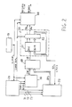
- Figure 2 shows in block diagram the digital apparatus object of the present invention.
- Figure 3 shows in timing diagram some signals present in the digital apparatus of Fig. 2.
- Figure 4 shows in a detailed diagram a preferred embodiment of a speed error measuring unit of the digital apparatus of fig. 2.
- Figure 5 shows in detailed diagram an alternative embodiment of speed error measuring unit and of speed error correction unit for the digital apparatus of fig. 2.
- Figure 1 shows in block diagram a typical data processing system comprising the digital apparatus of the present invention.
- Such apparatus, indicated by
reference number 1, is positioned between a drive device 2 for amass storage 2A and acontroller 3. - The system of fig. 1 further comprises a central processor 4, a peripheral controller 5 and a main memory 6.
- Central processor 4, main memory 6 and
controllers 3, 5 are connected each other by means of a plurality of leads orsystem bus 7 through which data, addresses and control signals can be exchanged. - In the present embodiment assumption is made that the system mass storage is provided with a 5 1/4 inch diskette and that drive device 2 is constituted by a disk driver.
- The consideration made in the following will be, however, valid for other kinds of storage devices too, as for instance, magnetic tape storages.
- In the present embodiment, where a mass storage is provided by a diskette, a standard circuit chip, such as the 1791 integrated circuit chip, manufactured by Western Digital Corporation, can be used as
controller 3. -
Controller 3 and drive device 2 exchange a plurality of control and information signals through a channel orbus 8. - Detailed description of the circuits and interface signals between
controller 3 and device 2 has been omitted since it is not essential for an understanding of the present invention. - In the case of the present invention embodiment a 5 1/4 inch diskette having been used for mass storage together with integrated circuit chip 1791 manufactured by Western Digital as controller, the circuits and interface signals can be drawn from the specifications of such products.
- The same considerations are valid for the interface between
controller 3 andrecovery apparatus 1. - It is only pointed out that the
recovery apparatus 1 must supplycontroller 3 with a square wave signal RDCLK and with a pulse train RD DATA atlogical level 0, each pulse corresponding to a magnetic flux transition detected on recording media. - Pulses RD DATA and window signal RD CLK have only to fulfill the condition that each pulse RD DATA occur entirely within a half wave (or window) of signal RD CLK.
- For the rest, the pulse position relative to window signal RD CLK and the pulse length can be arbitrary. However, it is preferred that the length of a pulse RD DATA fall in the range of 100 to 250 nsec. and the delay of the beginning or end of a pulse relative to the transition of window signal RD CLK should be no longer than 40 nsec.
-
Controller 3 does not need to be informed of whether each of the pulses RD DATA corresponds to a timing transition or to a data transition. The controller is able to distinguish between such transition from the pattern read out in response to the well known synchronization and "address mark" fields. - Also, the period of the timing or window signal can be variable and each of the two signals half waves may have a different length-Device 2 supplies
digital apparatus 1 with a pulse RAW DATA in response to each detected magnetic flux transition. Since the disclosed system is intended to recover FM and MFM recorded information, the time intervals between subsequent pulses RAW DATA are indicative of such information.Apparatus 1, in response to the pulse train RAW DATA received as an input, suppliescontroller 3 with the window signal RD CLK and with the pulses RD DATA which correspond to the pulses RAW DATA suitably positioned relative to window signal RD CLK.Controller 3 is able by means of signal RD CLK to detect the information bits within the pulse train RD DATA and make them available in parallel form tosystem bus 7. - Figure 2 shows in block diagram form, the
digital apparatus 1 of Fig- 1 which corresponds to the present invention.Apparatus 1 essentially comprises anoscillator 10, atiming unit 20, alogical unit 30 for measuring the interval duration between subsequent input pulses, alogical unit 40 for correcting such duration according to a speed difference as to a preestablished speed, alogic unit 50 for the peack shift recovery and the discrimination of the nominal duration corresponding to each interval, alogic unit 60 for reconstructing the read pulse train RD DATA within a window signal RD CLK generated byunit 60 itself and aunit 70 measuring and determining the speed difference as to a preestablished speed. - The reason why the measured speed error is referred to a preestablished speed instead of to the nominal speed will be explained later on.
-
Oscillator 10supplies units - Timing
unit 20 is activated by each of the pulses RAW DATA and supplies a plurality of timing signals REST, STOP, T1, T2, T3, LOAD OUT, tounits - Specifically signal LOAD OUT is sent to
units unit 30 and signals T1, T2, T3 are sent tounit 70. - Timing
unit 20 can be embodied in several ways, with shift registers, delay lines and particularly with the same components and connections shown in Fig. 3 of the already mentioned european patent application, therefore any further description is unnecessary. - For an easy understanding of the invention reference is made to Fig. 3 which shows in timing diagram the signals generated by the oscillator and by
unit 20 together with other signals which will be considered later on. - Diagram CLOCK is representative of signal CLOCK generated by
oscillator 10. - Diagram RAW DATA is representative of the read pulses received from
unit 20. The read pulses appear as aynchronous events as to signal CLOCK and at variable time intervals owing to the magnetic media speed errors and to the peak shift. - With the rise of signal CLOCK, immediately subsequent to the rise of signal RAW DATA, signal STOP rises to 1 and is kept at 1 for a duration of 19 CLOCK periods.
- When signal STOP falls to 0 a signal REST, normally at 1 falls to 0 for a duration of one CLOCK period.
- Signal LOAD OUT, T1, T2, T3 rise to logical level 1 for the duration of two CLOCK periods, respectively after 16,17,18,19 CLOCK periods from signal STOP rising.
- The sequence is triggered by pulse RAW DATA and, when the sequence is exhausted
unit 20 remains unactive until a new trigger pulse is received. - Measuring
unit 30 is constituted by a six cell binary counter (practically two integrated counters as shown in Fig. 4 of the already mentioned patent application) which is reset by signal REST atlogical level 0 and increments at each CLOCK pulse received on a clock input for the whole time signal STOP, applied to a control input, is at logical level O. -
Counter 3 stops when signal STOP is atlogical level 1. - Counter/
unit 30 supplies in output on a channel CNT a 6-bit binary code CNT1÷6 representative of the interval between the rising of two read pulses RAW DATA, expressed in CLOCK period number, less a fixed duration equal to 20 CLOCK periods (that is: 20•125 = 2500 nsec). - The measurement is affected by an uncertainty owing to the asynchronous raising of pulses RAW DATA as to the CLOCK pulses.
- The maximum value of such uncertainty is equal to two CLOCK periods that is 250 ns (±125nsec.).
-
Counter 30 is therefore able to measure, with a resolution of 250 nsec., time intervals varying from 2500 nsec. to 2500 + 125•(26-1) = = 10.375 nsec. - Binary code CNτ1÷6 remains unchanged for the whole time signal STOP is at
logical level 1 and is applied in input to speeddifference recovery unit 40 through channel CNT. - As shown in fig. 2
unit 40 consists of a permanent memory 41, having for instance a capacity of 2K bytes. - Six address input of memory 41 are connected to channel CNT and the remaining five are connected to a channel AV in output from
unit 70. A binary code AO-4 is present on channel AV representative of the speed difference as to the media nominal value. -
Memory 40 acts as transcoder and changes code CNT1÷6 received on channel CNT to a 5-bit code SR 1-5 representative of an interval duration between read pulses corrected in accordance to code AO-4 that is without speed error. - Code SR 1 -5 is applied, through channel SR, to peak
shift recovery unit 50. - As shown in fig. 2,
unit 50 is constituted by apermanent memory 51, having for instance a capacity of 2K bytes and by an 8-bit latch register 52. -
Memory 51 is provided with 11 address inputs I1÷11. - Five of them, 11 -5 receive code SR1÷5.
- The remaining 6 inputs 16=11 are connected to six of the eight outputs of
register 52. - The outputs of
memory 51 are connected to the inputs ofregister 52. - The information in output from
memory 51 is loaded intoregister 52 when the register is enabled by the rising edge of periodical signal LOAD OUT. - As widely discribed in the already mentioned european patent application, peak
shift recovery unit 50 operates as follows. -
Memory 51 is addressed by a code SR 1-5 representative of the measured actual duration DEN , corrected as concerns a possible speed error of an interval N between two read pulses n-1 and n. - It is further addressed in feedback by a 6-bit code - (received through register 52) representative in coded form of the entity and direction (positive or negative) of peak shifts PSn., of read pulse n-1.
- In other words, reminding that nominal duration DNN of interval N differs from duration DEN (corrected as concerns speed) owing to peak shifts PSn-1and PSn of read pulses n-1, n which define interval N, that is:

-
Memory 51 contains transcoding codes which perform such discrimination and, for each addressable position, that is for each pair of information DEN, PSn-1, supply in output the pair of information DNN, PSN, that is a 2 bit binary code Ao, Bo, specifying whether the nominal duration is 4, 6, 8, µsec., and a six bit binary code PS 1 -6, specifying with abit PS 1, if the peak shift is positive or negative and with the remaining bits the peak shift entity. - The codes A0, BO and
PS 1 +6 are loaded intoregister 52 and from there respectively sent to two inputs of unit 60 (code AO, BO) and to address inputs 16=11 ofmemory 51. - Further, lead 53 connects that
register 52 output on which information PS1 is present to an input ofunit 70. - It can be noted that peak
shift recovery unit 50 is quite identical (apart from connection 53) to and operates in the same way as the corresponding peak shift recovery unit described in the mentioned european patent application so that any detailed description is not required. - It is only to be pointed out that the transcoding codes recorded into
memory 51, in this case, may represent the actually detected entity of peak shift PS and not an information related to it (that is the actual duration of an interval DEN and the nominal duration DNNand DNN-1 of the same interval or of the preceding one) as disclosed by the mentioned application. - In fact such artifice, necessary to the mentioned application for avoiding the propagation and the accumulation of measurement errors is not required in the apparatus object of the present invention because, as disclosed later on,
unit 70 allows to recover such kind of error. -
Logic unit 60 timed by signals CLOCK and LOAD OUT, supplies in output according to code AO, A0, a timing window signal RD CLK and a data signal RD DATA, which can be detected by controller (Fig. 1). Sincelogic unit 60 is identical to the one disclosed by the mentioned application and -its description is unessential for the invention understanding, reference is made to the mentioned application for its architecture and operation details. - It is now considered, with reference to fig. 4 the speed
error recovery unit 70, actual object of the invention. -
Unit 70 comprises afirst counter 71, a secondbidirectional counter 72, aregister 73, apermanent memory 74, a NOTlogical element 75 and a two input logic ANDgate 76. -
Counter 71, for instance of the type available on the market with code 74LS169 is set for the cyclical reckoning of 8 pulses. - To this purpose its preset inputs corresponding to
binary weights 0, 2, 4, and its enabling input EN are connected to a logic level "0" source while preset input ofbinary weight 8 is connected to alogic level 1 source. - Input UP/DOWN is connected to a
logic level 0 source in order to increment. -
Counter 71 has a carry output CY normally atlogical level 1 which falls tological level 0 when the counter reaches its maximum counting status. - The CY output is connected to input LD of
counter 71 and its clock input receives timing pulses T3 fromunit 20. - When input LD is at
logical level 1, counter 71 increments at each rising edge of signal T3 applied to input CK. - When input LD is at
logic level 0 it is preset, on receipt of pulse T3 in the status established by the signals present on preset inputs. It is clear thatcounter 71, set in a binary status corresponding to 8, reaches binary status 15 on receipt of seven pulses T3 and at the reception of an eighth pulse T3 it is preset again. -
Counter 71 evolution is therefore cyclical with a period corresponding to the reception of 8 pulses T3 equal to 8 read intervals between read pulses. -
Counter 72, of the same type ofcounter 71, has its present input ofbinary weight 8 connected to a logic "1" while its preset inputs ofbinary weights 0, 2, 4 and its enabling input EN are connected to a logic "O". - Timing pulses T2, generated by
unit 20, are applied to CLOCK input CK. - Input LD is connected to carry output CY of
counter 71. - Input UP/DOWN of
counter 72 is connected to lead 53 and therefore periodically receives a signal indicating, with its logic level, if the last detected peak shift is positive or negative. - It is therefore clear that
counter 72 operates as follows. - At the end of a counter cycle of counter 71 -(CARRY = 0)
counter 72 is set into countingconfiguration 8 at reception of a first pulse T2 and subsequently at reception of seven subsequent pulses T2, increments or decrements according to whether during the interval between such pulses the signal onlead 53 is "1" or "0", that is according to whether the detected peak shift related to each of these intervals is positive or negative. - With the eight pulse T2 subsequent to the first one the counter is preset again to count
configuration 8. - The status reached by counter 72 at reception of the seventh pulses T2 therefore changes according to the number of negative or positive peak shift.
- In a period corresponding to seven read intervals, it is cleat that only the following cases can occur which lead to the binary status of the stated counter.
- The cases are shown in the following table for simplicity sake.

- From this table it clearly appears that the possible status reached by the counter are univocally established by the three most significant bits.
- The 3 most significant outputs of
counter 72 are connected to as many inputs of alatch register 73. - The register is periodically loaded, at the end of a counting cycle of
counters - To this purpose loading input LD of
counter 73 is connected to the output of ANDgate 76 which receives at a first input timing signal T1 and at a second input signal CY throughNOT 75. - Besides binary information representative of the counting status of counter 72 a binary information ΔV1÷5 representative of the speed error of the magnetic media as to the nominal speed is also loaded into
register 73. - The outputs of
register 73 are connected to as many address inputs ofpermanent memory 74 which, acting as transcoder, generates binary code ΔV1 ÷5 in output on channel AV. - This code is sent in feedback to the inputs of
register 73 as well as to corresponding address inputs of memory or speederror correction unit 40, as already explained. -
Unit 70 operates in conceptually simple way. - First of all it can be noted that
unit 70 generates in output a speed error code ΔV defining an actual speed of the magnetic media


- This information is used to correct the measured duration of the intervals between read pulses, therefore the corrected duration is affected by peak shift error only.
- On the other hand, in such a situation the peak shifts of the several pulses cannot accumulate that is, on average, during a certain number of subsequent read intervals, the peak shifts detected for the several read pulses must be positive and negative in equal number, that is their numerical difference must be zero or very near to zero.
- The consequence is that, if during a certain number of intervals between read pulses, in spite of the effected speed correction, the difference between positive and negative peak shifts (as detected by
counter 72 and in the following referenced with APS) is different from 0, the effected speed correction is not adequate and a speed error is still present - The pair of information APS and ΔV is used to address
memory 74 to a location generating in output a new speed error code ΔV' compensating such unadequacy. - It is clear that this compensation process also recover possible error accumulation due to the discrete nature of the duration measurement The compensation process takes place in a continuous periodic way with the updating of speed error ΔV at each period consisting of 8 intervals between subsequent read pulses, that is in the worst case of intervals with a nominal duration of 8 µsec. and a speed difference in defect of 10% each 70 usec., corresponding to a minimum frequency of 14KHertz.
- This frequency is much higher than the speed variation frequency of the magnetic media.
- The relationship between the pair of information ΔPS, ΔV and the new updated code ΔV' can be widely chosen.
- Practically, to secure stability to the conceptual implemented control loop it is suitable that the gain of the loop be lower than 1, that is the correcting action be not higher than the cause giving rise to it and that new value ΔV` differ from the previous one only for values of ΔPS equal to ±5, ±7. The relation may even be non linear.
- For instance, if code ΔV is constituted by 5 bits and can assume 32 different values representative of speed errors in a range field of ±12% (as to the nominal speed) and different the one from the other of multiples of an elementary quantity equal to about 0,8%, it can be imposed that if ΔPS=±5, ΔV' differs from ΔV of ±1,6% and if ΔPS = ±7 ΔV' differs from ΔV of ±3,2%.
- This means that a speed variation or error of 10% requires, to be integrally recovered, three measuring period that is, in the worst case 210 µsec., shorter than the wave quarter period of a speed variation with
frequency 1 KHz. - Figures 2 and 4 shows a preferred embodiment of the apparatus object of the present invention. Several changes can be made without departing from the scope of the invention.
- Fig. 5 shows a possible variant which can be used to minimize the number of permanent memories which are used.
- Particularly it shows
unit 70 andunit 40, the other elements of the apparatus remaining unchanged. - In this
case memory 74 of fig. 4 is substituted bymemory 40 in its operation. -
Register 73 latches ΔP generated bycounter 72, together with code AV, in this case a three bit code representative of the previously measured speed error. - The outputs of
register 73 are connected to corresponding address inputs ofmemory 40receiving code CNT 1 ÷6 on the other address inputs.Memory 40, according to the address codes, generates in output a code SR 1-5 with duration corrected as to the speed error and a new three bit code ΔV' representative of a new speed error updated according to code APS. - It is clear that, in this case the capacity of
memory 40 must be of 4K bytes and that the speed error AV is expressed with a lower resolution as to the one which can be obtained in the previously mentioned case. - However, it has been experimentally verified that this lower resolution does not substantially hamper the performances of the apparatus, and that in case a two bit code is used to express speed error AV (with consequent reduction of the memory capacity to 2K bytes) satisfactory performances are still obtained.
- The same considerations can be applied to code ΔPS which can be constituted by only two bits instead of 3 bits, by cutting the peak shifts counting to a lesser number of intervals, for
instance 3 or 5. - If the number of counted peak shifts is 3, it is clear that ΔPS can assume values +3, +1, -1, -3 which can be represented with a 2 bit code.
- If the number of counted peak shifts is 5, ΔPS can clearly assume values + 5, + 3, + 1, -1, -3, -5.
- With a suitable preset of
counter 72 and with a suitable choice of the output bits, values +3, + can be represented with the same code and values -1 -3 with another code, therefore assigning to values ΔPS=±3 ±1 the same connecting function (minimum or nul in absolute value) and to values APS±5 an higher correcting function. - It is also possible to increase the correction system resolution by increasing the number of bits constituting information ΔPS or ΔV and consequently increasing permanent memory 74 (fig. 4) or 40 capacity.
Claims (3)
characterized by that it comprises:
Applications Claiming Priority (2)
| Application Number | Priority Date | Filing Date | Title |
|---|---|---|---|
| IT20007/85A IT1200426B (en) | 1985-03-21 | 1985-03-21 | DIGITAL APPARATUS FOR RECOVERY SYSTEM OF BINARY INFORMATION RECORDED ON MAGNETIC MEDIA |
| IT2000785 | 1985-03-21 |
Publications (3)
| Publication Number | Publication Date |
|---|---|
| EP0195368A2 true EP0195368A2 (en) | 1986-09-24 |
| EP0195368A3 EP0195368A3 (en) | 1987-12-23 |
| EP0195368B1 EP0195368B1 (en) | 1990-03-07 |
Family
ID=11163062
Family Applications (1)
| Application Number | Title | Priority Date | Filing Date |
|---|---|---|---|
| EP86103372A Expired - Lifetime EP0195368B1 (en) | 1985-03-21 | 1986-03-13 | Digital apparatus for data recovery system |
Country Status (5)
| Country | Link |
|---|---|
| US (1) | US4714968A (en) |
| EP (1) | EP0195368B1 (en) |
| JP (1) | JPS61239465A (en) |
| DE (1) | DE3669411D1 (en) |
| IT (1) | IT1200426B (en) |
Cited By (4)
| Publication number | Priority date | Publication date | Assignee | Title |
|---|---|---|---|---|
| EP0222132A2 (en) * | 1985-10-10 | 1987-05-20 | BULL HN INFORMATION SYSTEMS ITALIA S.p.A. | Digital data separator |
| EP0222133A2 (en) * | 1985-10-10 | 1987-05-20 | BULL HN INFORMATION SYSTEMS ITALIA S.p.A. | Digital data separator |
| EP0300826A2 (en) * | 1987-07-22 | 1989-01-25 | Sharp Kabushiki Kaisha | Digital data detector |
| AU606409B2 (en) * | 1987-05-28 | 1991-02-07 | Apple Computer, Inc. | Disk drive controller |
Families Citing this family (5)
| Publication number | Priority date | Publication date | Assignee | Title |
|---|---|---|---|---|
| US4851932A (en) * | 1988-01-29 | 1989-07-25 | Storage Technology Corporation | Adaptive compensation circuit for moving data storage media |
| US5212445A (en) * | 1991-02-13 | 1993-05-18 | Seagate Technology, Inc. | Method and apparatus for detection and identification of flaws in a magnetic medium by measuring the width of pulses stored on the medium |
| US5335118A (en) * | 1992-07-22 | 1994-08-02 | Seagate Technology, Inc. | Disc drive with write precompensation using window/pulse timing measurements |
| JP3345515B2 (en) * | 1994-08-31 | 2002-11-18 | アイワ株式会社 | Peak shift correction circuit and magnetic recording medium reproducing apparatus using the same |
| JP3521239B2 (en) * | 1994-12-20 | 2004-04-19 | シャープ株式会社 | Disk drive device |
Citations (7)
| Publication number | Priority date | Publication date | Assignee | Title |
|---|---|---|---|---|
| FR2217757A1 (en) * | 1973-02-08 | 1974-09-06 | Siemens Ag | |
| US3864735A (en) * | 1973-09-12 | 1975-02-04 | Burroughs Corp | Read/write system for high density magnetic recording |
| EP0012880A1 (en) * | 1978-12-21 | 1980-07-09 | International Business Machines Corporation | Method of decoding phase-encoded, frequency-modulation encoded and modified-frequency modulation encoded binary data |
| GB2049370A (en) * | 1979-05-14 | 1980-12-17 | Honeywell Inf Systems | Data recovery systems |
| EP0034055A2 (en) * | 1980-02-06 | 1981-08-19 | Sperry Corporation | Variable window data recovery apparatus and method |
| GB2080658A (en) * | 1980-07-11 | 1982-02-03 | Tokyo Shibaura Electric Co | Input data synchronizing circuit |
| US4344039A (en) * | 1979-03-13 | 1982-08-10 | Sanyo Electric Co., Ltd. | Demodulating circuit for self-clocking-information |
Family Cites Families (2)
| Publication number | Priority date | Publication date | Assignee | Title |
|---|---|---|---|---|
| US4245264A (en) * | 1979-07-19 | 1981-01-13 | Control Systems, Inc. | Apparatus and method for digitally synchronizing the timing of a sequence of electrical output pulses in accordance with a selectable, permissably non-linear function of the timing of a sequence of electrical input pulses |
| US4281356A (en) * | 1979-11-28 | 1981-07-28 | R. C. Sanders Technology Systems, Inc. | Magnetic disk memory |
-
1985
- 1985-03-21 IT IT20007/85A patent/IT1200426B/en active
-
1986
- 1986-03-03 US US06/835,415 patent/US4714968A/en not_active Expired - Fee Related
- 1986-03-13 DE DE8686103372T patent/DE3669411D1/en not_active Expired - Lifetime
- 1986-03-13 EP EP86103372A patent/EP0195368B1/en not_active Expired - Lifetime
- 1986-03-20 JP JP61063871A patent/JPS61239465A/en active Pending
Patent Citations (7)
| Publication number | Priority date | Publication date | Assignee | Title |
|---|---|---|---|---|
| FR2217757A1 (en) * | 1973-02-08 | 1974-09-06 | Siemens Ag | |
| US3864735A (en) * | 1973-09-12 | 1975-02-04 | Burroughs Corp | Read/write system for high density magnetic recording |
| EP0012880A1 (en) * | 1978-12-21 | 1980-07-09 | International Business Machines Corporation | Method of decoding phase-encoded, frequency-modulation encoded and modified-frequency modulation encoded binary data |
| US4344039A (en) * | 1979-03-13 | 1982-08-10 | Sanyo Electric Co., Ltd. | Demodulating circuit for self-clocking-information |
| GB2049370A (en) * | 1979-05-14 | 1980-12-17 | Honeywell Inf Systems | Data recovery systems |
| EP0034055A2 (en) * | 1980-02-06 | 1981-08-19 | Sperry Corporation | Variable window data recovery apparatus and method |
| GB2080658A (en) * | 1980-07-11 | 1982-02-03 | Tokyo Shibaura Electric Co | Input data synchronizing circuit |
Non-Patent Citations (2)
| Title |
|---|
| ELECTRONIC DESIGN, vol. 28, no. 18, 1st September 1980, pages 168-169, Waseca MN, Denville NJ, US; B. RUGGIRELLO: "Wide effective margin makes double-density recording reliable" * |
| ELECTRONIC DESIGN, vol. 31, no. 9, April 1983, pages 207-210, Waseca MN, Denville NJ, US; H. ASSARPOUR: "Floppy-disk interface chip cuts parts, adds control" * |
Cited By (7)
| Publication number | Priority date | Publication date | Assignee | Title |
|---|---|---|---|---|
| EP0222132A2 (en) * | 1985-10-10 | 1987-05-20 | BULL HN INFORMATION SYSTEMS ITALIA S.p.A. | Digital data separator |
| EP0222133A2 (en) * | 1985-10-10 | 1987-05-20 | BULL HN INFORMATION SYSTEMS ITALIA S.p.A. | Digital data separator |
| EP0222132A3 (en) * | 1985-10-10 | 1988-10-26 | Honeywell Bull Italia S.P.A. | Digital data separator |
| EP0222133A3 (en) * | 1985-10-10 | 1988-10-26 | Honeywell Bull Italia S.P.A. | Digital data separator |
| AU606409B2 (en) * | 1987-05-28 | 1991-02-07 | Apple Computer, Inc. | Disk drive controller |
| EP0300826A2 (en) * | 1987-07-22 | 1989-01-25 | Sharp Kabushiki Kaisha | Digital data detector |
| EP0300826A3 (en) * | 1987-07-22 | 1990-05-09 | Sharp Kabushiki Kaisha | Digital data detector |
Also Published As
| Publication number | Publication date |
|---|---|
| DE3669411D1 (en) | 1990-04-12 |
| JPS61239465A (en) | 1986-10-24 |
| IT1200426B (en) | 1989-01-18 |
| EP0195368B1 (en) | 1990-03-07 |
| IT8520007A0 (en) | 1985-03-21 |
| EP0195368A3 (en) | 1987-12-23 |
| US4714968A (en) | 1987-12-22 |
Similar Documents
| Publication | Publication Date | Title |
|---|---|---|
| USRE33665E (en) | Digital signal detecting and compensating circuit with adjustable window signal | |
| US4425646A (en) | Input data synchronizing circuit | |
| US4644420A (en) | Circuit and methodology for reading and tracking binary data from magnetic tape independently of the data pattern on the tape | |
| EP0544358B1 (en) | Phase locked loop with frequency deviation detector and decoder circuit comprising such a phase locked loop | |
| US4596981A (en) | Synchronizing signal detecting circuit in a digital signal transmitting system | |
| US4423498A (en) | Control apparatus for a recording medium drive motor in a digital information reproducing apparatus | |
| KR870000515B1 (en) | Frequency detecting circuit | |
| US4449061A (en) | Wave-shaping circuit for digital signal | |
| NL8602418A (en) | DEVICE FOR DISPLAYING A PCM MODULATED SIGNAL WITH A MUTE CIRCUIT. | |
| EP0195368B1 (en) | Digital apparatus for data recovery system | |
| SE451926B (en) | SIGNALVAGSSTYRKRETS | |
| US4672482A (en) | Digital apparatus for magnetic media data recovery system | |
| US4344039A (en) | Demodulating circuit for self-clocking-information | |
| US5386405A (en) | Disk apparatus having a read error retry function | |
| US5526333A (en) | Optical disk recording device | |
| US5892631A (en) | Method and an arrangement for detecting state transitions in a read signal during a bit cell timing window | |
| US6580775B1 (en) | Method of detecting frequency of digital phase locked loop | |
| US4742403A (en) | Digital data separator | |
| CA1169152A (en) | Circuit for decoding a diphase signal | |
| EP0110105A1 (en) | Systems for reading magnetic recordings | |
| EP0222133B1 (en) | Digital data separator | |
| US4298956A (en) | Digital read recovery with variable frequency compensation using read only memories | |
| US6895174B2 (en) | Frame number detecting device | |
| EP0428411B1 (en) | Information processing apparatus | |
| US4331985A (en) | Splicing-point detection apparatus and method |
Legal Events
| Date | Code | Title | Description |
|---|---|---|---|
| PUAI | Public reference made under article 153(3) epc to a published international application that has entered the european phase |
Free format text: ORIGINAL CODE: 0009012 |
|
| AK | Designated contracting states |
Kind code of ref document: A2 Designated state(s): DE FR GB NL |
|
| PUAL | Search report despatched |
Free format text: ORIGINAL CODE: 0009013 |
|
| RAP1 | Party data changed (applicant data changed or rights of an application transferred) |
Owner name: HONEYWELL BULL ITALIA S.P.A. |
|
| AK | Designated contracting states |
Kind code of ref document: A3 Designated state(s): DE FR GB NL |
|
| 17P | Request for examination filed |
Effective date: 19880212 |
|
| RAP1 | Party data changed (applicant data changed or rights of an application transferred) |
Owner name: BULL HN INFORMATION SYSTEMS ITALIA S.P.A. |
|
| 17Q | First examination report despatched |
Effective date: 19890615 |
|
| GRAA | (expected) grant |
Free format text: ORIGINAL CODE: 0009210 |
|
| AK | Designated contracting states |
Kind code of ref document: B1 Designated state(s): DE FR GB NL |
|
| REF | Corresponds to: |
Ref document number: 3669411 Country of ref document: DE Date of ref document: 19900412 |
|
| ET | Fr: translation filed | ||
| PLBE | No opposition filed within time limit |
Free format text: ORIGINAL CODE: 0009261 |
|
| STAA | Information on the status of an ep patent application or granted ep patent |
Free format text: STATUS: NO OPPOSITION FILED WITHIN TIME LIMIT |
|
| 26N | No opposition filed | ||
| PGFP | Annual fee paid to national office [announced via postgrant information from national office to epo] |
Ref country code: FR Payment date: 19920326 Year of fee payment: 7 |
|
| PGFP | Annual fee paid to national office [announced via postgrant information from national office to epo] |
Ref country code: NL Payment date: 19920331 Year of fee payment: 7 |
|
| PGFP | Annual fee paid to national office [announced via postgrant information from national office to epo] |
Ref country code: DE Payment date: 19930219 Year of fee payment: 8 |
|
| PGFP | Annual fee paid to national office [announced via postgrant information from national office to epo] |
Ref country code: GB Payment date: 19930302 Year of fee payment: 8 |
|
| PG25 | Lapsed in a contracting state [announced via postgrant information from national office to epo] |
Ref country code: NL Effective date: 19931001 |
|
| NLV4 | Nl: lapsed or anulled due to non-payment of the annual fee | ||
| PG25 | Lapsed in a contracting state [announced via postgrant information from national office to epo] |
Ref country code: FR Effective date: 19931130 |
|
| REG | Reference to a national code |
Ref country code: FR Ref legal event code: ST |
|
| PG25 | Lapsed in a contracting state [announced via postgrant information from national office to epo] |
Ref country code: GB Effective date: 19940313 |
|
| GBPC | Gb: european patent ceased through non-payment of renewal fee |
Effective date: 19940313 |
|
| PG25 | Lapsed in a contracting state [announced via postgrant information from national office to epo] |
Ref country code: DE Effective date: 19941201 |