EP0193447B1 - Static numerical circuit interrupter having a calibration circuit - Google Patents
Static numerical circuit interrupter having a calibration circuit Download PDFInfo
- Publication number
- EP0193447B1 EP0193447B1 EP86400281A EP86400281A EP0193447B1 EP 0193447 B1 EP0193447 B1 EP 0193447B1 EP 86400281 A EP86400281 A EP 86400281A EP 86400281 A EP86400281 A EP 86400281A EP 0193447 B1 EP0193447 B1 EP 0193447B1
- Authority
- EP
- European Patent Office
- Prior art keywords
- value
- analog
- multiplexer
- signal
- digital
- Prior art date
- Legal status (The legal status is an assumption and is not a legal conclusion. Google has not performed a legal analysis and makes no representation as to the accuracy of the status listed.)
- Expired - Lifetime
Links
Images


Classifications
-
- H—ELECTRICITY
- H02—GENERATION; CONVERSION OR DISTRIBUTION OF ELECTRIC POWER
- H02H—EMERGENCY PROTECTIVE CIRCUIT ARRANGEMENTS
- H02H1/00—Details of emergency protective circuit arrangements
- H02H1/0038—Details of emergency protective circuit arrangements concerning the connection of the detecting means, e.g. for reducing their number
-
- H—ELECTRICITY
- H02—GENERATION; CONVERSION OR DISTRIBUTION OF ELECTRIC POWER
- H02H—EMERGENCY PROTECTIVE CIRCUIT ARRANGEMENTS
- H02H3/00—Emergency protective circuit arrangements for automatic disconnection directly responsive to an undesired change from normal electric working condition with or without subsequent reconnection ; integrated protection
- H02H3/08—Emergency protective circuit arrangements for automatic disconnection directly responsive to an undesired change from normal electric working condition with or without subsequent reconnection ; integrated protection responsive to excess current
- H02H3/093—Emergency protective circuit arrangements for automatic disconnection directly responsive to an undesired change from normal electric working condition with or without subsequent reconnection ; integrated protection responsive to excess current with timing means
- H02H3/0935—Emergency protective circuit arrangements for automatic disconnection directly responsive to an undesired change from normal electric working condition with or without subsequent reconnection ; integrated protection responsive to excess current with timing means the timing being determined by numerical means
-
- H—ELECTRICITY
- H02—GENERATION; CONVERSION OR DISTRIBUTION OF ELECTRIC POWER
- H02H—EMERGENCY PROTECTIVE CIRCUIT ARRANGEMENTS
- H02H3/00—Emergency protective circuit arrangements for automatic disconnection directly responsive to an undesired change from normal electric working condition with or without subsequent reconnection ; integrated protection
- H02H3/02—Details
- H02H3/05—Details with means for increasing reliability, e.g. redundancy arrangements
Definitions
- the present invention aims to allow the realization of a digital static trigger with high dynamics using low resolution components.
- the trip device is characterized in that it comprises a calibration circuit having an input receiving said analog signal and developing on at least four output channels four analog signals whose values are in a predetermined ratio, and an addressable multiplexer four inputs of which are connected to the four channels of the calibration circuit and the output of which is connected to the input of the analog digital converter, the calibration circuit comprising at least two amplifiers having a predetermined gain ratio, the output of each amplifier being connected on the one hand to an input of the multiplexer and on the other hand to a divider bridge whose midpoint is connected to another input of the multiplexer, the multiplexer being controlled by the microprocessor to select one of said channels, compatible with the dynamics of the digital analog converter, the output signal of said multiplexer being a continuous measurement of the says analog signal.
- the input of the 8-bit digital analog converter is connected to a multiplexer with six inputs addressable by the microprocessor. Four inputs are reserved for the phase fault signal and two inputs for the earth fault signal.
- a diode protection circuit limits the voltage on the input of the multiplexer to a value compatible with the characteristics of the multiplexer.
- Document US-A 4 470 092 describes a microprocessor motor protection in which the phase current signal is applied to a circuit comprising two different gain amplifiers so as to provide two different sensitivity outputs. These two outputs are applied to two inputs of a multiplexer and the microprocessor sequentially reads all of the inputs of the multiplexer and enters the data present on these inputs into a table for further processing.
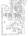
- an electrical distribution network with four conductors RSTN for supplying a load comprises a circuit breaker 10 capable of interrupting the circuit in the open position.
- the mechanism 12 of the circuit breaker 10 is controlled by a polarized relay 14, for controlling the tripping of the circuit breaker in the event of an overload, short-circuit or earth fault.
- Each phase conductor RST is associated with a current transformer 16, which delivers a signal proportional to the current flowing through the associated conductor, the signal being applied to a rectifier bridge 18, at full alternation.
- the outputs of the three rectifier bridges 18 are connected in series in a circuit, comprising in series a resistor 20, a Zener diode 22 and a diode 24 to make appear at the terminals of the resistor 20 a voltage signal, proportional to the maximum value of the current flowing through the conductors RST and at the terminals of the diodes 22 , 24 a supply voltage for electronic circuits.
- the voltage signal is applied to the inputs of two amplifiers 26, 28 of different gains and the output of each amplifier 26, 28 is connected on the one hand to an input 1, 3 of a multiplexer 29 and on the other hand to a divider bridge 30, 32, the midpoint of which is connected to an input 2, 4 of the multiplexer 29.
- the assembly, amplifiers 26, 28 and divider bridges 30, 32 belongs to a circuit for calibrating the voltage signal 34, described in detail below and marked in broken lines in Figure 1.
- the calibration circuit 34 comprises a third amplifier 36, which receives a signal generated by the summing transformer 38, the primary windings of which consist of the NRST conductors passing through a toroid, carrying a secondary winding 40 which delivers a signal in the event of a fault at Earth.
- the output of amplifier 36 is connected to input 5 of multiplexer 29 and to a divider bridge 41, the midpoint of which is connected to input 6 of multiplexer 29.
- Inputs 1 to 6 are connected in parallel by diodes 44 to the emitter of a transistor 42 whose collector is grounded and whose base is biased by a predetermined voltage, for example 5 Volts, corresponding to the maximum value applicable to the multiplexer 29.
- the multiplexer 29 receives signals representative of the phase current on the four inputs 1 to 4 and signals representative of the earth current on the two inputs 5, 6. These signals, in particular those of earth fault, can of course be developed in a different way, for example from the signals delivered by the current transformers 16.
- the multiplexer 29 for example an ADC0808 multiplexer from the company National Semiconductor, is controlled by the address and control line 46 connected to the outputs 1 of a microprocessor 48. Depending on the address provided by the microprocessor 48 the signal from one of the inputs 1 - 6 of the multiplexer 29 is transmitted by the output S of the multiplexer 29 to an analog digital converter 50 with 8 bits.
- a bus 52 connects the output of the digital analog converter 50 to an input, output 2 of the microprocessor 48.
- a block 54 with eight multiplexed switches 72-86 is connected to the microprocessor 48, on the one hand by a connection to the bus 52 and on the other hand in 3 by an address link 56. Each switch 72-86 has eight distinct positions for adjusting the trigger parameters, described below.
- An output register 58 is connected to the microprocessor 48 by a 6-bit link 60 and a 1-bit link 62 for transmission on 7 output channels S1 to S7 of command and signaling orders.
- the output S1 is connected to the relay 14 to control tripping of the circuit breaker 10, while the outputs S2 to S6 are connected to display means of a control panel 64, arranged on the front face of the circuit breaker, in particular of the block trip unit containing all of the fault trip circuits and components.
- the S7 output is connected to an analog trip command described below.
- a non-volatile ROM memory 66 is connected to a link 4 of the microprocessor 48 to supply it with the execution program as well as permanent data stored in the form of tables.
- the recorded program corresponds to the functions executed by the trigger.
- the same trigger can be designed for several ranges of functions and each range obviously corresponds to a particular program.
- the program chosen can be saved in the ROM memory during manufacture or according to a preferred embodiment, the different programs are saved in different memories, the trigger being personalized by the choice of the appropriate memory, during assembly.
- the easements, grouped in a block 68 connected to an input 5 of the microprocessor 48, include the circuits necessary for the operation of the microprocessor, in particular the clock for sequencing the sequence of instructions, the initialization circuits and the like.
- the microprocessor is for example the model MC 146805 sold by the company Motorola, which contains standard resources, such as the processing unit, the interfaces, the volatile RAM memories, the computing unit.
- Block 70 receives the analog phase signal at the output of the rectifier bridges 18.
- Block 70 compares this signal with a predetermined threshold value, in order to emit a tripping order transmitted to relay 14, when crossing the threshold as described in detail below.
- Block 70 provides a faster trigger speed than that of the digital trigger.
- FIG. 1 and the corresponding description contain the elements essential to the functioning of the trigger, the accessory elements of the analog and digital parts, such as the power supplies, the resistors and bias capacitors, the registers and memories of the fugitive signals, having been omitted so as not to unnecessarily overload the description.
- the control panel 64 has eight switches 72-86 which are the eight switches of the block 54 illustrated in FIG. 1. Each eight-position switch cooperates with a resistive network to select one of the eight distinct values, transmitted to the microprocessor 48 during of the interrogation of block 54.
- the panel 64 also has five light-emitting diodes or LEDs 90-98 and a connector 88 of a test block.
- the trigger can be used for two types of function. a protection function against phase and earth fault and a protection function against phase fault and a load shedding function.
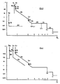
- FIG. 3 illustrates, on a logarithmic scale, the tripping curves of the phase and earth protection.
- the long delay threshold ILR that is to say the intensity of the current beyond which the long delay tripping cycle is initiated, is adjustable by the switch 80.
- the long delay time delay can be adjusted by switch 78 which modifies the constant T1.
- the trigger starts a short delay trigger cycle, which anticipates the long delay trigger.
- the switch 84 performs the adjustment of the short delay ICR threshold and the switch 82 that of the constant short delay time delay T3.
- the passage from the characteristic at constant time to that at inverse time is fixed at a constant value of the current.
- the instantaneous analog trip device 70 intervenes in normal operation for an ultra-fast opening of the circuit breaker 10.
- an overload threshold Is appears, with an abscissa slightly lower than that of the long delay threshold ILR, the crossing of which signals the proximity of the long delay threshold and the risk of tripping.
- Switch 76 sets the overload threshold ls. This signal for crossing the threshold Is can be used for a simplified load shedding command, in this case breaking a non-priority circuit. As soon as the current falls below the Is threshold, the output is deactivated and the unloaded circuit is reconnected.
- the earth protection representative curve includes an earth protection threshold IP and a time delay T5 at constant time.
- the IP threshold is adjustable by switch 74 and the timer T5 by switch 72.
- the status of the trip unit at a given time is displayed on the panel 64 by the light-emitting diodes or LEDs 90-98, represented on the curves of FIG. 3.
- the LED 90 represented by a solid circle on the earth protection threshold IP, is lit when a circuit breaker 10 trips on an earth fault. It remains lit until the moment of an external intervention, for example of rearming.
- the indicator 92 represented by four alternately white and black circular sectors, lights up when the overload threshold Is is crossed and goes off automatically as soon as the current falls below this threshold.
- the crossing of the long delay ILR threshold is signaled by the warning light 94, which goes out if the current value decreases below this threshold before the end of the time delay.
- a tripping on overload, controlled by the long delay circuit, is signaled by the warning light 96 while a short delay and instantaneous tripping causes the warning light 98 to light up.
- the extinction of the warning lights 96, 98 requires an external action.
- the adjustment precision can be increased by the use of switches 72-86 having a greater number of positions or according to a preferred mode by a combination of two adjustment means, more particularly of the switch 76 and of the other adjustment switches. Such a combination gives 64 setting notches, the switch 76 playing a double role, made possible by a sufficient gap between the thresholds Is and ILR. It is conceivable to add independent switches to achieve this type of combination.
- the same device can be used for another protection version, illustrated by the curves in FIG. 4.
- the phase protection tripping curve is identical to that illustrated in FIG. 3, but the earth protection is not not insured.
- the switches 72, 74 and the indicators 90, 92 associated with this function are available and the software is modified to provide a load shedding and shedding function illustrated by curves 106, 108.
- the load shedding threshold IDE lower than the long delay threshold ILR, is adjustable by switch 72, the light 90 signaling a load shedding operation.
- the IRE load shedding threshold which is different and lower than the IDE load shedding threshold, is adjustable by the switch 74 and indicated by the indicator 92.
- the load shedding curve 106 is in inverse time parallel to the long delay protection curve 100, while the Relestation curve 108 is at constant time. The settings must always ensure load shedding before a long delay trip.
- the different protections and functions of the trip unit require current measurement with great dynamics.
- a dynamic of 0.4 In In being the nominal current
- 12 In for the highest instantaneous trip threshold, ie a ratio of 30.
- the number representing 0.4 ln must have at least the value 100, which is equivalent to a value of 3000 for the maximum intensity of 12 In.
- the number 3000 requires coding 12-bit, but a 12-bit digital analog converter is slow and expensive.
- the calibration circuit 34 adapts the dynamics of the analog chain to that of the digital analog converter 50 to 8 bits while respecting the precision of 1%.
- the gain of amplifier 26 is chosen to transform an analog signal, corresponding to a maximum current of 14 In, applied to its input into a maximum signal, for example of 5 Volts, appearing on channel 2 of input of the multiplexer 29 which will be digitized by the value 256 at the output of the digital analog converter 50.
- the divider bridge 30, of a ratio 2 applies on channel 1 a double signal and the maximum value of 5 Volts is not exceeded as long as the analog signal at the input of the amplifier 26 remains less than 7 In.
- the amplifier 28 applies to the input 4 of the multiplexer 29 a maximum signal for a value of 1.7 ln of the current and at input 3 a maximum signal for a value of 0.85 In. It is easy to see that the gain ratio of the amplifiers 26, 28 is 8.
- the microprocessor 48 selects one of the channels 1 to 4 depending on the value of the current, in this case channel 2 for a co urant between 7 and 14 In, channel 1 for a current between 1.7 and 7 ln, channel 4 for a current between 0.85 and 1.7 ln, and channel 3 for a current less than 0 , 85 In.
- the microprocessor 48 multiplies the digitization by a factor taking into account the selected channel, to restore the initial magnitude of the signal.
- the microprocessor 48 activates channel 2 (14 In) and digitizes the corresponding signal. If the result is greater than the value 128, the digitization is multiplied by 16 and stored in a RAM memory. If the result is less than 128, the digitization is performed on channel 1 (7 In) and when the result is greater than 64, the digitization is multiplied by 8 and the result is saved in the memory. When the result is less than 64, you digitize on channel 4 (1.7 In) and if the digitization is greater than 128, you multiply it by 2 before storing it in memory. For a result lower than 128 the digitization is carried out on channel 3 (0.85 In) and the result is stored directly in the memory.
- the dynamics of the 50 to 8 bit digital analog converter is thus adapted to the range of variation of the currents from 0.4 ln to 12 ln while ensuring sufficient precision. It should be noted that the number of channels and thereby the number of calibers can be increased for greater precision or amplitude of variation or conversely this number of channels can be reduced - otherwise.
- the earth fault signal is likely to be applied to the 2 channels 5 and 6 only.
- the dynamic range of this signal is less than that of the phase fault and the two calibers are sufficient.
- the selection of the two channels 5, 6 by the microprocessor 48 is carried out in the manner described above, which it is unnecessary to recall.
- the transition from the analog channel to the digital channel results in a sampling of the processed signals.
- the value of the digital signal remains constant for the duration of the sample and this duration is determined by the sampling period fixed by the microprocessor 48. This duration, for example 1.84 milliseconds, must be compared with the duration of 10 milliseconds of an alternation of the alternating signal and it is clear that the error introduced by the sampling is not negligible.
- the timing diagram according to FIG. 6a shows on the one hand the variation curve 110 of an analog signal rectified at full alternation, as a function of time and on the other hand, the curve 112 of the corresponding sample available at the output of the converter analog digital 50.
- the chronometric selectivity is achieved when the non-tripping time of the upstream circuit breaker is greater than the tripping time, that is to say the total breaking time of the downstream circuit breaker.
- the tripping and non-tripping curves, of the type illustrated in Figures 3 and 4, of circuit breakers in series, must be offset enough to avoid any intersection of these curves.
- the specialist is well aware of these problems of selectivity and the advantage of a difference as small as possible between the trigger and non-trigger times to interrupt the fault current as quickly as possible while maintaining the supply to the healthy parts of the 'installation.
- the precision of the sampled peak value is increased by blocking and memorizing the last peak and by processing this blocked value at the half peak to ensure the protection functions.
- FIG. 7 represents the flowchart of processing: At time t1 the microprocessor 48 calls and processes the sampled signal for measuring the intensity MESURI delivered by the digital analog converter 50 (fig. 6a). This MESURI signal is compared to the INTPHA signal (fig. 6d) of stored phase intensity, blocked at the last peak. If MESURI is greater than INTPHA the peak value is increasing and the value DERCRE (fig. 6b), which represents the value of the last peak less than the INTPHA signal, is set to zero.
- the MESURI value is stored in the MESURI-1 memory (fig. 6c) as well as in the INTPHA memory (fig. 6d).
- the TEMPEC value (fig. 6e), which manages the countdown, is set to the maximum and the INTPHA value is processed by the microprocessor 48 in the aforementioned manner to ensure the protection functions.
- the measurements MESURI and MESURI-1 are compared. At time t2 the measurement MESURI is not greater than MESURI-1 and the value MESURI is entered in the memory MESURI-1. Then we check if TEMPEC is equal to zero, which is not the case at time t2 and we decrease TEMPEC.
- the INTPHA intensity is treated to ensure the protective function.
- the measurement MESURI is always less than the intensity INTPHA, but it is greater than MESURI-1 (increasing phase).
- MESURI-1 increasing phase
- the peak sampled value of the second half-wave is lower than that of the first altemance and it can be seen that the stored value INTPHA retained for the processing is the highest peak value.
- the two half-waves of the analog signal are identical, the difference of the peak sampled values resulting from the sampling.
- the value of the second peak is temporarily stored in the DERCRE memory.
- MESURI again exceeds INTPHA and in the manner described for the first altemance DERCRE is reset, MESURI replacing the value MESURI-1 and INTPHA in the memory.
- TEMPEC is reset to the maximum value and the new peak sampled value INTPHA is blocked.
- the processed value, stored in INTPHA corresponds to the sampled value blocked at the last peak, the countdown being restarted at each again exceeding the peak value.
- This blocked value takes into account at least two peak values for an alternating current of 50 Hz, the duration of each alternation of which is 10 milliseconds. If during the 22 milliseconds the peak values remain lower than the blocked peak value INTPHA, the latter is replaced by the value DERCRE which is the last blocked peak value less than INTPHA.
- the processed signal immediately takes this increase into account, while at decrease there is a time delay of 22 milliseconds.
- Locking at the last peak has no influence on instantaneous triggering, but for short delay and long delay triggering it allows a reduction of the sampling error.
- the 22 millisecond delay can cause an unjustified trigger, but the influence is weak considering the delays of the order of one second of such triggers.
- the 22 milliseconds are a compromise between greater precision on the peak value and as small a difference as possible between the trigger and non-trigger times. It is clear that the time delay can be increased to include a greater number of alternations and thus increase the accuracy, in particular when measuring or displaying the peak value independently of the control of the circuit breaker.
- the method of blocking at the last peak has been described above for a phase fault, but it is used with the same advantages for earth protection.
- the inverse function 1 2 t constant, represented by the straight line 100 in FIG. 3, of long delay triggering, is equivalent to that of the bimetallic strip of a conventional trigger which heats up when the current is above a first threshold and is cools if the current is below this threshold.
- This inverse function is carried out by calculating a thermal image of a bimetal strip represented by a stored digital value. During the heating phase this stored value is increased by a predetermined factor to translate the heating, while this stored value is decremented during a cooling phase. Triggering occurs when the stored value exceeds a threshold. This thermal image makes it possible to take account of the previous state and to faithfully translate the temperature of the bimetallic strip or of the device protected by the circuit breaker.
- the long delay inverse function is carried out by the microprocessor program 48, illustrated in FIG. 8 and described below.
- the INTPHA intensity is the aforementioned value of the PHAse INTensity blocked at the last peak.
- the microprocessor 48 compares the INTPHA value with the ILR threshold displayed by the switch 80. If the intensity INTPHA is not greater than the ILR threshold, the overload bit, which feeds the indicator 94, is set to zero, the indicator 94 thus being extinguished.
- MULRR multiplier factor
- this multiplier is initialized to a number determined by the position of the long delay timer switch 78 and a value TETALR (temperature TETA of a simulated bimetal for the long delay function) recorded in the RAM memory, is multiplied by a reduction factor representative of the cooling of the equivalent bimetallic strip, the new value TETALR being substituted for the old one in the memory. This sequence corresponds to a cooling of the bimetallic strip.
- a warm-up phase starts when the INTPHA intensity becomes greater than the ILR threshold.
- MULRE multiplier factor
- the MULRE multiplier is decremented and the program is terminated. If the MULRE multiplier is equal to zero, the overload bit goes to 1 to light the indicator 94 and the MULRE multiplier is initialized to a number determined by the switch 78.
- An arithmetic and logic unit of the microprocessor 48 executes a setting operation.
- the role of the multiplying factors MULRR and MULRE is the adjustment of the rate of incrementation or decrementation of the digitized thermal image.
- adjusting the multipliers to the number three causes an operation, once out of three, which results in a time delay three times longer. These multipliers allow a choice of the long delay trigger curve.
- the short delay inverse time function is performed in an analogous manner by the flowchart according to FIG. 9. If the intensity INTPHA is less than the ICR threshold, the temperature of a simulated bimetallic strip for the short delay function TETACR is multiplied by a reduction factor representative of the cooling and the new value is entered into the RAM memory. If the intensity INTPHA exceeds the ICR threshold, it is checked whether the square of the sampled current blocked at the last peak DTETACR, which corresponds to the heating, is greater than a given maximum value, of stop BUTCR, corresponding to the passage of the trigger in time inverse to the triggering of the short delay function at constant time.
- the value TETACR is replaced in the memory by the incremented value TETACR + DTETACR and it is checked whether this new value TETACR exceeds the trigger threshold TETACRMAX. In the event of an overshoot, a tripping order is transmitted to relay 14 ensuring short time protection with reverse time. When the temperature rise DTETACR is greater than the stop value BUTCR this latter value is substituted for DTETACR and added to the value TETACR in the aforementioned manner to cause a trip or not depending on whether the new value TETACR representing the simulated bimetal temperature controller is higher or lower than the TETACRMAX threshold.
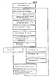
- FIG 10 shows the main trigger program.
- the microprocessor 48 acquires the adjustment parameters introduced by the switches 72-86 of the block 54. Then it reads the value of the phase current and of the earth current supplied by the multiplexer 29, all of this data being recorded in the memory. RAM. The microprocessor 48 then proceeds to the blocking sampling at the last peak of the phase current and of the earth current as described above. It then processes the instantaneous function by checking whether the phase current blocked at the last peak exceeds the instantaneous trip threshold IIN or not.
- the program is then subdivided into two branches traversed alternately, the first consisting in the calculation of the square of the current necessary for the determination of the inverse time function and the second in the successive processing of the long delay, short delay and earth protection function .
- This separation of treatments allows a reduction in the duration of the program to a value of 1.84 milliseconds.
- the signaling and triggering instructions are issued and a new cycle is executed after waiting for synchronization respecting the cycle time of 1.84 milliseconds.
- the operation of the digital processing trip unit mentioned above is imperfect during a significant short circuit and during the start-up period.
- Digital processing is fast, but not instantaneous and this delay can in certain cases be the cause of the destruction of the protected installation and / or the circuit breaker.
- the digital processing chain is shunted by an analog processing chain to provide additional instantaneous protection.
- the rectified signal, proportional to the current in the RST conductors and present at the output of the rectifier bridges 18, is processed in the analog block 70, to generate an instantaneous tripping order transmitted to the relay 14 when a predetermined threshold is exceeded. Referring more particularly to FIG.
- the signal applied to the input of block 70 is amplified in an operational amplifier 114 whose output is connected to an input of a comparator 116, whose output is connected to relay 14.
- the other input of comparator 116 is connected to point 118 of a bridge divider with two resistors 120, 122 in series.
- Parallel to the resistor 122 is connected a shunting circuit constituted by a resistor 124 and a transistor 126 in series.
- the transistor 126 is controlled by an order issued on the output S7 of the register 58 to interrupt or close the shunting circuit.
- the divider bridge 120, 122 and the shunting circuit 124, 126 determine two different thresholds IR, IR1 according to the blocking or the conduction of the transistor 126, the comparator 116 comparing the signal with these thresholds to emit the trigger order when these thresholds are crossed.
- the threshold IR is greater than the digital instantaneous trigger threshold IIN, the threshold IR1 being slightly less than or equal to the threshold IIN.
- the IR threshold is selected during activation of the S7 output, in this case during operation of the digital processing chain. If the digital chain is not activated, the intervention threshold of the analogue chain is reduced to the value IR1.
- the analog trip unit does not intervene, overloads and short-circuits being dealt with by the digital trip unit.
- the operating threshold of the analog trigger is set to the IR value and only a short circuit of an exceptional value greater than the IR threshold, is treated by the two chains, the analog chain anticipating the digital chain and controlling the triggering. This quick trip ensures protection of the circuit breaker.
- the digital chain is inactive for a short start-up period and the threshold of the analog trip unit 70 is automatically reduced to the lower value IR1 by the absence of the signal on the output S7.
- the analog trip unit operates as soon as the IR1 threshold is exceeded, protecting both the circuit breaker and the installation.
- the analog chain also makes up for a failure in the digital chain and increases the reliability of the release without any noticeable complication. It should be noted that the threshold change of the analog trigger can be carried out in a different way.
- the trigger combines the advantages of analog triggers and digital triggers without significant complications.
Landscapes
- Emergency Protection Circuit Devices (AREA)
- Keying Circuit Devices (AREA)
- Measurement Of Current Or Voltage (AREA)
- Driving Mechanisms And Operating Circuits Of Arc-Extinguishing High-Tension Switches (AREA)
- Breakers (AREA)
- Elimination Of Static Electricity (AREA)
Abstract
Description
L'invention est relative à un déclencheur statique numérique pour un disjoncteur électrique comprenant :
- - des capteurs de courant qui engendrent des signaux analogiques proportionnels aux courants parcourant les conducteurs protégés par le disjoncteur,
- - des circuits redresseurs pour redresser lesdits signaux et délivrer un signal continu analogique représentatif de la valeur maximale desdits courants,
- - un convertisseur analogique digital ayant une entrée recevant ledit signal analogique et une sortie délivrant un signal numérisé échantillonné correspondant,
- - un ensemble de traitement numérique à microprocesseur, auquel est appliqué le signal numérisé pour assurer une fonction de déclenchement long retard et une fonction de déclenchement court retard, et qui élabore un ordre de déclenchement du disjoncteur, lors d'un dépassement de seuils prédéterminés, ledit ordre étant temporisé en fonction de la valeur du signal,
- - et un moyen de déclenchement du disjoncteur activé par ledit ordre de déclenchement.
- - current sensors which generate analog signals proportional to the currents flowing through the conductors protected by the circuit breaker,
- rectifier circuits for rectifying said signals and delivering an analog continuous signal representative of the maximum value of said currents,
- an analog digital converter having an input receiving said analog signal and an output delivering a corresponding sampled digitized signal,
- - a digital microprocessor processing unit, to which the digitized signal is applied to ensure a long delay tripping function and a short delay tripping function, and which develops a tripping order for the circuit breaker, when predetermined thresholds are exceeded, said order being timed as a function of the value of the signal,
- - And a circuit breaker trip means activated by said trip order.
Le développement des microprocesseurs a permis la mise en oeuvre, dans les déclencheurs de disjoncteurs électriques, des techniques numériques, dont la fiabilité et les possibilités de réglage et d'adaptation à un nombre important de fonctions sont bien connues. La grande dynamique des courants de défaut traités par le déclencheur, dont le rapport peut être de 30 et la précision de déclenchement imposée, impliquent des nombres représentatifs de valeur élevée, par exemple codés sur 12 bits. Les composants à 12 bits, notamment les convertisseurs analogiques digitaux à 12 bits sont chers et lents, et cet handicap limite les possibilités d'emploi de cette technologie.The development of microprocessors has made it possible to use digital techniques in trip devices for electrical circuit breakers, the reliability of which and the possibilities of adjustment and adaptation to a large number of functions are well known. The large dynamic range of fault currents processed by the trip device, the ratio of which can be 30 and the trip accuracy required, imply representative numbers of high value, for example coded on 12 bits. 12-bit components, especially 12-bit digital analog converters are expensive and slow, and this handicap limits the possibilities of using this technology.
La présente invention vise à permettre la réalisation d'un déclencheur statique numérique à grande dynamique faisant usage de composants de faible résolution.The present invention aims to allow the realization of a digital static trigger with high dynamics using low resolution components.
Le déclencheur selon l'invention est caractérisé en ce qu'il comporte un circuit de calibrage ayant une entrée recevant ledit signal analogique et élaborant sur au moins quatre voies de sorties quatre signaux analogiques dont les valeurs sont dans un rapport prédéterminé, et un multiplexeur adressable dont quatre entrées sont reliées aux quatre voies du circuit de calibrage et dont la sortie est reliée à l'entrée du convertisseur analogique digital, le circuit de calibrage comportant au moins deux amplificateurs ayant un rapport de gains prédéterminé, la sortie de chaque amplificateur étant reliée d'une part à une entrée du multiplexeur et d'autre part à un pont diviseur dont le point milieu est relié à une autre entrée du multiplexeur, le multiplexeur étant piloté par le microprocesseur pour sélectionner l'une desdites voies, compatible avec la dynamique du convertisseur analogique digital, le signal de sortie dudit multiplexeur étant une mesure continue dudit signal analogique.The trip device according to the invention is characterized in that it comprises a calibration circuit having an input receiving said analog signal and developing on at least four output channels four analog signals whose values are in a predetermined ratio, and an addressable multiplexer four inputs of which are connected to the four channels of the calibration circuit and the output of which is connected to the input of the analog digital converter, the calibration circuit comprising at least two amplifiers having a predetermined gain ratio, the output of each amplifier being connected on the one hand to an input of the multiplexer and on the other hand to a divider bridge whose midpoint is connected to another input of the multiplexer, the multiplexer being controlled by the microprocessor to select one of said channels, compatible with the dynamics of the digital analog converter, the output signal of said multiplexer being a continuous measurement of the says analog signal.
Selon un mode de réalisation préféré, l'entrée du convertisseur analogique digital à 8 bits est réliée à un multiplexeur à six entrées adressables par le microprocesseur. Quatre entrées sont réservées au signal de défaut de phase et deux entrées au signal de défaut de terre. Un circuit de protection à diodes limite la tension sur l'entrée du multiplexeur à une valeur compatible avec les caractéristiques du multiplexeur.According to a preferred embodiment, the input of the 8-bit digital analog converter is connected to a multiplexer with six inputs addressable by the microprocessor. Four inputs are reserved for the phase fault signal and two inputs for the earth fault signal. A diode protection circuit limits the voltage on the input of the multiplexer to a value compatible with the characteristics of the multiplexer.
Le document US-A 4 470 092 décrit une protection de moteur à microprocesseur dans laquelle le signal de courant phase est appliqué à un circuit comportant deux amplificateurs de gains différents de manière à fournir deux sorties de sensibilité différentes. Ces deux sorties sont appliquées à deux entrées d'un multiplexeur et le microprocesseur lit sé- quentiellement toutes les entrées du multiplexeur et introduit les données présentes sur ces entrées dans une table pour un traitement ultérieur.Document US-A 4 470 092 describes a microprocessor motor protection in which the phase current signal is applied to a circuit comprising two different gain amplifiers so as to provide two different sensitivity outputs. These two outputs are applied to two inputs of a multiplexer and the microprocessor sequentially reads all of the inputs of the multiplexer and enters the data present on these inputs into a table for further processing.
D'autres avantages et caractéristiques ressortiront plus clairement de la description qui va suivre d'un mode de mise en oeuvre de l'invention, donné à titre d'exemple non limitatif et représenté aux dessins annexés, dans lesquels :
- - la figure 1 est un schéma bloc du déclencheur selon l'invention;
- - la figure 2 montre la face avant du déclencheur avec les moyens de réglage et de signalisation;
- - les figures 3 et 4 représentent les courbes de déclenchement de deux versions du déclencheur selon l'invention;
- - la figure 5 est l'organigramme de la fonction de changement de calibre;
- - la figure 6 montre la variation des signaux traités par le microprocesseur pour les fonctions à temps inverse;
- - la figure 7 est l'organigramme de la fonction de blocage à la dernière crête;
- - la figure 8 est l'organigramme de la fonction long retard à temps inverse;
- - la figure 9 est l'organigramme de la fonction court retard à temps inverse;
- - la figure 10 est l'organigramme de la fonction générale de déclenchement;
- - la figure 11 est le schéma de détail de la chaîne de traitement analogique.
- - Figure 1 is a block diagram of the trigger according to the invention;
- - Figure 2 shows the front face of the trigger with the adjustment and signaling means;
- - Figures 3 and 4 show the release curves of two versions of the release according to the invention;
- - Figure 5 is the flowchart of the caliber change function;
- - Figure 6 shows the variation of the signals processed by the microprocessor for the inverse time functions;
- - Figure 7 is the flowchart of the blocking function at the last peak;
- - Figure 8 is the flow diagram of the long delay function with inverse time;
- - Figure 9 is the flow diagram of the short delay function with inverse time;
- - Figure 10 is the flowchart of the general trigger function;
- - Figure 11 is the detailed diagram of the analog processing chain.
Sur la figure 1, un réseau de distribution électrique à quatre conducteurs RSTN d'alimentation d'une charge (non représentée) comporte un disjoncteur 10 susceptible d'interrompre le circuit en position d'ouverture. Le mécanisme 12 du disjoncteur 10 est piloté par un relais 14 polarisé, de commande de déclenchement du disjoncteur en cas de surcharge, de court-circuit ou de défaut à la terre. A chaque conducteur de phase RST est associé un transformateur de courant 16, qui délivre un signal proportionnel au courant parcourant le conducteur associé, le signal étant appliqué à un pont redresseur 18, à double alternance. Les sorties des trois ponts redresseurs 18 sont connectées en série dans un circuit, comprenant en série une résistance 20, une diode Zener 22 et une diode 24 pour faire apparaître aux bornes de la résistance 20 un signal de tension, proportionnel à la valeur maximale du courant parcourant les conducteurs RST et aux bornes des diodes 22, 24 une tension d'alimentation des circuits électroniques. Le signal de tension est appliqué aux entrées de deux amplificateurs 26, 28 de gains différents et la sortie de chaque amplificateur 26, 28 est reliée d'une part à une entrée 1, 3 d'un multiplexeur 29 et d'autre part à un pont diviseur 30, 32, dont le point milieu est connecté à une entrée 2, 4 du multiplexeur 29. L'ensemble, amplificateurs 26, 28 et ponts diviseurs 30, 32, appartient à un circuit de calibrage 34 du signal de tension, décrit en détail ci-dessous et repéré en trait discontinu sur la figure 1.In FIG. 1, an electrical distribution network with four conductors RSTN for supplying a load (not shown) comprises a
Le circuit de calibrage 34 comporte un troisième amplificateur 36, qui reçoit un signal engendré par le transformateur sommateur 38, dont les enroulements primaires sont constitués par les conducteurs NRST traversant un tore, portant un enroulement secondaire 40 qui délivre un signal en cas de défaut à la terre. La sortie de l'amplificateur 36 est connectée à l'entrée 5 du multiplexeur 29 et à un pont diviseur 41, dont le point milieu est relié à l'entrée 6 du multiplexeur 29. Les entrées 1 à 6 sont connectées en parallèle par des diodes 44 à l'émetteur d'un transistor 42 dont le collecteur est mis à la masse et dont la base est polarisée par une tension prédéterminée, par exemple de 5 Volts, correspondant à la valeur maximale applicable au multiplexeur 29. Il est facile de voir que le multiplexeur 29 reçoit des signaux représentatifs du courant de phase sur les quatre entrées 1 à 4 et des signaux représentatifs du courant de terre sur les deux entrées 5, 6. Ces signaux, notamment ceux de défaut de terre, peuvent bien entendu être élaborés d'une manière différente, par exemple à partir des signaux délivrés par les transformateurs de courant 16.The
Le multiplexeur 29, par exemple un multiplexeur ADC0808 de la société National Semiconductor, est piloté par la ligne d'adresse et de contrôle 46 reliée aux sorties 1 d'un microprocesseur 48. En fonction de l'adresse fournie par le microprocesseur 48 le signal de l'une des entrées 1 - 6 du multiplexeur 29 est transmis par la sortie S du multiplexeur 29 à un convertisseur analogique digital 50 à 8 bits. Un bus 52 relie la sortie du convertisseur analogique digital 50 à une entrée, sortie 2 du microprocesseur 48. Un bloc 54 à huit commutateurs 72-86 multiplexés est relié au microprocesseur 48, d'une part par une connexion au bus 52 et d'autre part en 3 par une liaison d'adresse 56. Chaque commutateur 72-86 présente huit positions distinctes de réglage des paramètres de déclenchement, décrits par la suite.The
Un registre 58 de sortie est relié au microprocesseur 48 par une liaison 60 à 6 bits et une liaison 62 à 1 bit pour une transmission sur 7 voies de sorties S1 à S7 des ordres de commande et de signalisation. La sortie S1 est reliée au relais 14 pour commander le déclenchement du disjoncteur 10, tandis que les sorties S2 à S6 sont connectées à des moyens d'affichage d'un panneau de commande 64, disposé sur la face avant du disjoncteur, notamment du bloc déclencheur contenant l'ensemble des circuits et composants de commande de déclenchement sur défaut. La sortie S7 est reliée à une commande de déclenchement analogique décrite ci-dessous.An
Une memoire ROM 66 non volatile est reliée à une liaison 4 du microprocesseur 48 pour lui fournir le programme d'exécution ainsi que des données permanentes rangées sous forme de tableaux. Le programme enregistré correspond aux fonctions exécutées par le déclencheur. Un même déclencheur peut être conçu pour plusieurs gammes de fonctions et à chaque gamme correspond bien entendu un programme particulier. Le programme choisi peut être enregistré dans la mémoire ROM à la fabrication ou selon un mode de réalisation préférentiel, les différents programmes sont enregistrés dans différentes mémoires, te déclencheur étant personnalisé par le choix de la mémoire appropriée, lors du montage. Les servitudes, groupées dans un bloc 68 relié à une entrée 5 du microprocesseur 48, comprennent les circuits nécessaires au fonctionnement du microprocesseur, notamment l'horloge pour le sé- quencement du déroulement des instructions, les circuits d'initialisation et analogues.A
Le microprocesseur est par exemple le modèle MC 146805 commercialisé par la société Motorola, qui contient les ressources standard, tels que l'unité de traitement, les interfaces, les mémoires RAM volatiles, l'unité de calcul.The microprocessor is for example the model MC 146805 sold by the company Motorola, which contains standard resources, such as the processing unit, the interfaces, the volatile RAM memories, the computing unit.
A la commande numérique de déclenchement décrite ci-dessus est associé un bloc 70 de déclenchement instantané conventionnel, recevant le signal analogique de phase à la sortie des ponts redresseurs 18. Le bloc 70 compare ce signal à une valeur de seuil prédéterminée, pour émettre un ordre de déclenchement transmis au relais 14, lors du franchissement du seuil de la manière décrite en détail ci-dessous. Le bloc 70 assure une rapidité de déclenchement supérieure à celle du déclencheur numérique.With the digital triggering control described above is associated a conventional
Il convient de noter que la figure 1 et la description correspondante contiennent les éléments essentiels au fonctionnement du déclencheur, les éléments accessoires des parties analogique et numérique, telles que les alimentations, les résistances et condensateurs de polarisation, les registres et mémoires des signaux fugitifs, ayant été omis pour ne pas surcharger inutilement la description.It should be noted that FIG. 1 and the corresponding description contain the elements essential to the functioning of the trigger, the accessory elements of the analog and digital parts, such as the power supplies, the resistors and bias capacitors, the registers and memories of the fugitive signals, having been omitted so as not to unnecessarily overload the description.
Le panneau de commande 64 comporte huit commutateurs 72-86 qui sont les huit commutateurs du bloc 54 illustré par la figure 1. Chaque commutateur à huit positions coopère avec un réseau résistif pour sélectionner l'une des huit valeurs distinctes, transmises au microprocesseur 48 lors de l'interrogation du bloc 54. Le panneau 64 présente de plus cinq diodes électroluminescentes ou voyants 90-98 et un connecteur 88 d'un bloc de test.The
Le déclencheur peut être utilisé pour deux types de fonction. une fonction de protection sur défaut de phase et de terre et une fonction de protection sur défaut de phase et une fonction de délestage.The trigger can be used for two types of function. a protection function against phase and earth fault and a protection function against phase fault and a load shedding function.
La figure 3 illustre, à échelle logarithmique, les courbes de déclenchement de la protection de phase et de terre.FIG. 3 illustrates, on a logarithmic scale, the tripping curves of the phase and earth protection.
Le seuil long retard ILR, c'est-à-dire l'intensité du courant au-delà de laquelle le cycle de déclenchement long retard est amorcé, est réglable par le commutateur 80. Le temps après lequel le disjoncteur déclenche est fonction de l'intensité du courant, la relation étant à temps inverse, 12t = T1 = constante, qui en coordonnées logarithmiques se traduit par le segment de droite inclinée 100. La temporisation long retard peut être réglée par le commutateur 78 qui modifie la constante T1.The long delay threshold ILR, that is to say the intensity of the current beyond which the long delay tripping cycle is initiated, is adjustable by the
Si l'intensité du courant franchit un deuxième seuil, en l'occurrence le seuil court retard ICR, le déclencheur démarre un cycle de déclenchement court retard, qui devance le déclenchement long retard. La courbe représentative du déclenchement court retard comprend deux segments successifs, le segment 102 à temps inverse, représenté par la relation 12t = T2, et le segment 104 à temps constant T3. Le commutateur 84 réalise le réglage du seuil court retard ICR et le commutateur 82 celui de la temporisation constante court retard T3. Le passage de la caractéristique à temps constant à celle à temps inverse est fixé à une valeur constante du courant.If the current intensity crosses a second threshold, in this case the short delay ICR threshold, the trigger starts a short delay trigger cycle, which anticipates the long delay trigger. The curve representing the short delay tripping comprises two successive segments, the
Un troisième seuil, IIN, supérieur au seuil ICR et réglable par le commutateur 86, provoque le cycle de déclenchement instantané, dont la temporisation T4 correspond au temps de réponse du déclencheur qui n'est pas réglable.A third threshold, IIN, greater than the ICR threshold and adjustable by the
Au-dessus d'un quatrième seuil IR intervient en fonctionnement normal le déclencheur instantané analogique 70 pour une ouverture ultra-rapide du disjoncteur 10.Above a fourth IR threshold, the instantaneous
Sur la figure 3 apparaît de plus un seuil de surcharge Is, d'abscisse légèrement inférieure à celle du seuil long retard ILR, dont le franchissement signale la proximité du seuil long retard et le risque d'un déclenchement. Le commutateur 76 règle le seuil de surcharge ls. Ce signal de franchissement du seuil Is peut être utilisé pour une commande de délestage simplifiée, en l'occurrence de coupure d'un circuit non prioritaire. Dès que le courant redevient inférieur au seuil Is, la sortie est désactivée et le circuit délesté est rebranché.In FIG. 3, an overload threshold Is appears, with an abscissa slightly lower than that of the long delay threshold ILR, the crossing of which signals the proximity of the long delay threshold and the risk of tripping. Switch 76 sets the overload threshold ls. This signal for crossing the threshold Is can be used for a simplified load shedding command, in this case breaking a non-priority circuit. As soon as the current falls below the Is threshold, the output is deactivated and the unloaded circuit is reconnected.
La courbe représentative de la protection de terre comprend un seuil protection de terre IP et une temporisation T5 à temps constant. Le seuil IP est réglable par le commutateur 74 et la temporisation T5 par le commutateur 72.The earth protection representative curve includes an earth protection threshold IP and a time delay T5 at constant time. The IP threshold is adjustable by
L'état du déclencheur à un instant donné est visualisé sur le panneau 64 par les diodes électroluminescentes ou voyants 90-98, représentées sur les courbes de la figure 3. Le voyant 90, représenté par un rond plein sur le seuil de protection de terre IP, est allumé lors d'un déclenchement du disjoncteur 10 sur un défaut de terre. Il reste allumé jusqu'au moment d'une intervention externe, par exemple de réarmement. Le voyant 92, représenté par quatre secteurs circulaires altemativement blancs et noirs, s'allume lors du franchissement du seuil de surcharge Is et s'éteint automatiquement dès que le courant redevient inférieur à ce seuil. Le franchissement du seuil long retard ILR est signalé par le voyant 94, qui s'éteint si la valeur du courant diminue en-dessous de ce seuil avant la fin de la temporisation. Un déclenchement sur surcharge, commandé par le circuit long retard, est signalé par le voyant 96 tandis qu'un déclenchement court retard et instantané provoque l'allumage du voyant 98. L'extinction des voyants 96, 98 nécessite une action externe. Ces techniques de réglage et d'affichage sont bien connues des spécialistes, et il est inutile de les décrire en détail. La précision de réglage peut être accrue par l'emploi de commutateurs 72-86 ayant un plus grand nombre de positions ou selon un mode préférentiel par une combinaison de deux moyens de réglage, plus particulièrement du commutateur 76 et des autres commutateurs de réglage. Une telle combinaison donne 64 crans de réglage, le commutateur 76 jouant un double rôle, rendu possible par un écart suffisant entre les seuils Is et ILR. Il est concevable d'adjoindre des commutateurs indépendants pour réaliser ce type de combinaisons.The status of the trip unit at a given time is displayed on the
Le même appareil est utilisable pour une autre version de protection, illustrée par les courbes de la figure 4. Dans cette version la courbe de déclenchement de protection de phase est identique à celle illustrée par la figure 3, mais la protection de terre n'est pas assurée. Les commutateurs 72, 74 et les voyants 90, 92 associés à cette fonction sont disponibles et le logiciel est modifié pour assurer une fonction de délestage et de relestage illustrée par les courbes 106, 108. Le seuil de délestage IDE, inférieur au seuil long retard ILR, est réglable par le commutateur 72, le voyant 90 signalant une opération de délestage. Le seuil de relestage IRE, différent et inférieur au seuil de délestage IDE, est réglable par le commutateur 74 et signalé par le voyant 92. La courbe de délestage 106 est à temps inverse parallèle à la courbe 100 de protection long retard, tandis que la courbe 108 de relestage est à temps constant. Les réglages doivent toujours assurer un délestage avant un déclenchement long retard.The same device can be used for another protection version, illustrated by the curves in FIG. 4. In this version the phase protection tripping curve is identical to that illustrated in FIG. 3, but the earth protection is not not insured. The
Les différentes protections et fonctions du déclencheur nécessitent la mesure du courant avec une grande dynamique. En globalisant on arrive à une dynamique de 0,4 In (In étant le courant nominal) pour le seuil long retard le plus bas et à 12 In pour le seuil de déclenchenent instantané le plus élevé, soit un rapport de 30. Pour obtenir une précision suffisante, notamment une résolution de 1 %, il faut que le nombre représentant 0,4 ln ait au moins la valeur 100, ce qui équivaut à une valeur de 3000 pour l'intensité maximale de 12 In. Le nombre 3000 nécessite un codage sur 12 bits, mais un convertisseur analogique digital à 12 bits est lent et cher.The different protections and functions of the trip unit require current measurement with great dynamics. By globalizing we arrive at a dynamic of 0.4 In (In being the nominal current) for the lowest long delay threshold and to 12 In for the highest instantaneous trip threshold, ie a ratio of 30. To obtain a sufficient accuracy, in particular a resolution of 1%, the number representing 0.4 ln must have at least the
Le circuit de calibrage 34 selon l'invention adapte la dynamique de la chaîne analogique à celle du convertisseur analogique digital 50 à 8 bits tout en respectant la précision de 1 %. A cet effet, le gain de l'amplificateur 26 est choisi pour transformer un signal analogique, correspondant à un courant maximal de 14 In, appliqué sur son entrée en un signal maximal, par exemple de 5 Volts, apparaissant sur la voie 2 d'entrée du multiplexeur 29 qui sera numérisé par la valeur 256 à la sortie du convertisseur analogique digital 50. Le pont diviseur 30, d'un rapport 2, applique sur la voie 1 un signal double et la valeur maximale de 5 Volts n'est pas dépassée tant que le signal analogique à l'entrée de l'amplificateur 26 reste inférieur à 7 In. D'une manière analogue, l'amplificateur 28 applique à l'entrée 4 du multiplexeur 29 un signal maximal pour une valeur de 1,7 ln du courant et à l'entrée 3 un signal maximal pour une valeur de 0,85 In. Il est facile de voir que le rapport des gains des amplificateurs 26, 28 est de 8. Le microprocesseur 48 sélectionne l'une des voies 1 à 4 en fonction de la valeur du courant, en l'occurrence la voie 2 pour un courant compris entre 7 et 14 In, la voie 1 pour un courant compris entre 1,7 et 7 ln, la voie 4 pour un courant compris entre 0,85 et 1,7 ln, et la voie 3 pour un courant inférieur à 0,85 In. Le microprocesseur 48 multiplie la numérisation par un facteur tenant compte de la voie sélectionnée, pour rétablir la grandeur initiale du signal.The
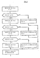
Le fonctionnement de ce circuit de calibrage ressort de l'organigramme illustré par la figure 5 :The operation of this calibration circuit is shown in the flow diagram illustrated in FIG. 5:
Le microprocesseur 48 active la voie 2 (14 In) et numérise le signal correspondant. Si le résultat est supérieur à la valeur 128 la numérisation est multipliée par 16 et rangée dans une mémoire RAM. Si le résultat est inférieur à 128, la numérisation est effectuée sur la voie 1 (7 In) et lorsque le résultat est supérieur à 64 on multiplie la numérisation par 8 et on énregistre le résultat dans la mémoire. Lorsque le résultat est inférieur à 64 on numérise sur la voie 4 (1,7 In) et si la numérisation est supérieure à 128 on la multiplie par 2 avant de la ranger dans la mémoire. Pour un résultat inférieur à 128 la numérisation est effectuée sur la voie 3 (0,85 In) et le résultat est rangé directement dans la mémoire. La dynamique du convertisseur analogique digital 50 à 8 bits est ainsi adaptée à la gamme de variation des courants de 0,4 ln à 12 ln en assurant une précision suffisante. Il est à noter que le nombre de voies et par là le nombre de calibres peut être augmenté pour une précision ou une amplitude de variation supérieure ou inversement ce nombre de voies peut être diminué-dans le cas contraire.The
En se référant à la figure 1, on voit que le signal de défaut de terre est susceptible d'être appliqué aux 2 voies 5 et 6 seulement. La dynamique de ce signal est inférieure à celle du défaut de phase et les deux calibres sont suffisants. La sélection des deux voies 5, 6 par le microprocesseur 48 s'effectue de la manière décrite ci-dessus, qu'il est inutile de rappeler.Referring to Figure 1, we see that the earth fault signal is likely to be applied to the 2
L'emploi selon l'invention du multiplexeur 29 et du circuit de calibrage 34 réalise d'une manière simple l'adaptation des dynamiques de la chaîne analogique et de la chaîne numérique.The use according to the invention of the
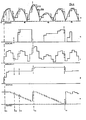
Le passage de la chaîne analogique à la chaîne numérique se traduit par un échantillonnage des signaux traités. La valeur du signal numérique reste constante pendant la durée de l'échantillon et cette durée est déterminée par la période d'échantillonnage fixée par le microprocesseur 48. Cette durée, par exemple de 1,84 millisecondes, doit être comparée à la durée de 10 millisecondes d'une alternance du signal alternatif et il est clair que l'erreur introduite par l'échantillonnage n'est pas négligeable. Le chronogramme selon la figure 6a montre d'une part la courbe de variation 110 d'un signal analogique redressé à double alternance, en fonction du temps et d'autre part, la courbe 112 de l'échantillon correspondant disponible à la sortie du convertisseur analogique digital 50. Ces courbes 110, 112 font ressortir l'erreur précitée, notamment sur la valeur crête des signaux, qui peut atteindre 10 %. L'importance de cette valeur crête, qui détermine le déclenchement et la temporisation au déclenchement, ressort de l'exposé précédent. L'erreur sur la mesure de la valeur crête se répercute sur la temporisation de déclenchement, et cette imprécision est particulièrement gênante pour la sélectivité de déclenchement. On sait que dans un réseau de distribution électrique plusieurs disjoncteurs sont connectés en série, les caractéristiques de déclenchement de ces disjoncteurs étant échelonnées de manière à assurer une sélectivité de déclenchement, seul le disjoncteur directement en amont du défaut s'ouvrant pour éliminer le défaut, les autres disjoncteurs restant fermés pour alimenter les branches saines du réseau. La sélectivité chronométrique est réalisée lorsque le temps de non-déclenchement du disjoncteur amont est supérieur au temps de déclenchement, c'est-à-dire au temps total de coupure du disjoncteur aval. Les courbes de déclenchement et de non-déclenchement, du type illustré par les figures 3 et 4, des disjoncteurs en série, doivent être décalées suffisamment pour éviter toute intersection de ces courbes. Le spécialiste connait bien ces problèmes de sélectivité et l'intérêt d'un écart aussi faible que possible entre les temps de déclenchement et de non-déclenchement pour interrompre le plus rapidement possible le courant de défaut en maintenant l'alimentation des parties saines de l'installation.The transition from the analog channel to the digital channel results in a sampling of the processed signals. The value of the digital signal remains constant for the duration of the sample and this duration is determined by the sampling period fixed by the
La précision de la valeur crête échantillonnée est accrue en bloquant et en mémorisant la dernière crête et en traitant cette valeur bloquée à la demiè- re crête pour assurer les fonctions de protection.The precision of the sampled peak value is increased by blocking and memorizing the last peak and by processing this blocked value at the half peak to ensure the protection functions.
Dans une mémoire RAM sont mémorisées les cinq valeurs représentées par les courbes des fig. 6 a, b, c, d, e, en l'occurrence : MESURI qui est la MESURe de lintensité de l'échantillon traité à un instant t.
- MESURI-1 qui est la MESURe de l'intensité de l'échantillon traité à un instant t-1.
- INTPHA qui est la valeur échantillonnée de l'INTensité de PHAse, bloquée à la dernière crête.
- DERCRE qui est la valeur de la DERnière CREte inférieure à la valeur INTPHA.
- TEMPEC qui est le TEMPs ECoulé géré en compte à rebours.
- MESURI-1 which is the MEASUREMENT of the intensity of the sample treated at an instant t-1.
- INTPHA which is the sampled value of the PHAse INTensity, blocked at the last peak.
- DERCRE which is the value of the LAST CRETE lower than the INTPHA value.
- TEMPEC which is the ELAPSED TEMPs managed in countdown.
La figure 7 représente l'organigramme de traitement : Au temps t1 le microprocesseur 48 appelle et traite le signal échantillonné de mesure de l'intensité MESURI délivré par le convertisseur analogique digital 50 (fig. 6a). Ce signal MESURI est comparé au signal INTPHA (fig. 6d) d'intensité de phase mémorisé, bloqué à la dernière crête. Si MESURI est supérieur à INTPHA la valeur crête est croissante et la valeur DERCRE (fig. 6b), qui représente la valeur de la dernière crête inférieure au signal INTPHA, est mise à zéro.FIG. 7 represents the flowchart of processing: At time t1 the
La valeur MESURI est enregistrée dans la mémoire MESURI-1 (fig. 6c) ainsi que dans la mémoire INTPHA (fig. 6d). La valeur TEMPEC (fig. 6e), qui gère le compte à rebours, est mise au maximum et la valeur INTPHA est traitée par le microprocesseur 48 de la manière susmentionnée pour assurer les fonctions de protection.The MESURI value is stored in the MESURI-1 memory (fig. 6c) as well as in the INTPHA memory (fig. 6d). The TEMPEC value (fig. 6e), which manages the countdown, is set to the maximum and the INTPHA value is processed by the
Si la mesure MESURI est inférieure à l'intensité INTPHA, par exemple au temps t2 correspondant à la phase descendante du signal analogique, on compare les mesures MESURI et MESURI-1. Au temps t2 la mesure MESURI n'est pas supérieure à MESURI-1 et on introduit la valeur MESURI dans la mémoire MESURI-1. Puis on vérifie si TEMPEC est égale à zéro, ce qui n'est pas le cas au temps t2 et on décrémente TEMPEC. L'intensité INTPHA est traitée pour assurer la fonction de protection.If the measurement MESURI is less than the intensity INTPHA, for example at time t2 corresponding to the falling phase of the analog signal, the measurements MESURI and MESURI-1 are compared. At time t2 the measurement MESURI is not greater than MESURI-1 and the value MESURI is entered in the memory MESURI-1. Then we check if TEMPEC is equal to zero, which is not the case at time t2 and we decrease TEMPEC. The INTPHA intensity is treated to ensure the protective function.
Au temps t3 correspondant à la phase montante de l'altemance suivante la mesure MESURI est toujours inférieure à l'intensité INTPHA, mais elle est supérieure à MESURI-1 (phase croissante). On compare la mesure MESURI à la crête DERCRE et comme MESURI est supérieure à DERCRE on introduit la valeur MESURI dans la mémoire avant de poursuivre le programme précité d'introduction de la valeur MESURI dans la mémoire MESURI-1 et les autres opérations. Dans l'exemple selon la figure 6, la valeur crête échantillonnée de la deuxième alternance est inférieure à celle de la première altemance et on voit que la valeur mémorisée INTPHA retenue pour le traitement est la valeur crête la plus élevée. En réalité les deux alternances du signal analogique sont identiques, la différence des valeurs crêtes échantillonnées résultant de l'échantillonnage. Par le blocage à la dernière crête, en l'occurrence en retenant la première valeur de crête la plus élevée à la place de la seconde, l'erreur est notablement réduite. La valeur de la deuxième crête est stockée temporairement dans la mémoire DERCRE.At time t3 corresponding to the rising phase of the following altemance, the measurement MESURI is always less than the intensity INTPHA, but it is greater than MESURI-1 (increasing phase). We compare the measurement MESURI to the peak DERCRE and as MESURI is greater than DERCRE we enter the value MESURI in the memory before continuing the aforementioned program of introduction of the value MESURI in the memory MESURI-1 and the other operations. In the example according to FIG. 6, the peak sampled value of the second half-wave is lower than that of the first altemance and it can be seen that the stored value INTPHA retained for the processing is the highest peak value. In reality the two half-waves of the analog signal are identical, the difference of the peak sampled values resulting from the sampling. By blocking at the last peak, in this case by retaining the first highest peak value instead of the second, the error is significantly reduced. The value of the second peak is temporarily stored in the DERCRE memory.
Au temps t4 de la troisième alternance, MESURI dépasse à nouveau INTPHA et de la manière décrite pour la première altemance DERCRE est remise à zéro, MESURI remplaçant la valeur MESURI-1 et INTPHA dans la mémoire. TEMPEC est remise à la valeur maximale et la nouvelle valeur crête échantillonnée INTPHA est bloquée.At time t4 of the third alternation, MESURI again exceeds INTPHA and in the manner described for the first altemance DERCRE is reset, MESURI replacing the value MESURI-1 and INTPHA in the memory. TEMPEC is reset to the maximum value and the new peak sampled value INTPHA is blocked.
L'amplitude des alternances 4 et 5 est inférieure à celle de la troisième alternance et le compte à rebours se poursuit normalement jusqu'au temps t5 de passage à zéro. En se référant à l'organigramme on voit que si TEMPEC est égale à zéro et que DERCRE est différente de zéro, ce qui est le cas en t5, la valeur DERCRE remplace dans la mémoire la valeur INTPHA et DERCRE est mise à zéro.The amplitude of
Il est facile de comprendre que pendant la durée du compte à rebours, TEMPEC qui est par exemple de 22 millisecondes, la valeur traitée, mémorisée dans INTPHA, correspond à la valeur échantillonnée bloquée à la dernière crête, le compte à rebours étant recommencé à chaque nouveau dépassement de la valeur crête. Cette valeur bloquée tient compte d'au moins deux valeurs crêtes pour un courant alternatif de 50 Hz dont la durée de chaque alternance est de 10 millisecondes. Si pendant les 22 millisecondes les valeurs crêtes restent inférieures à la valeur crête bloquée INTPHA, cette dernière est remplacée par la valeur DERCRE qui est la dernière valeur crête bloquée inférieure à INTPHA. A la croissance des valeurs crêtes le signal traité tient immédiatement compte de cette augmentation tandis qu'à la décroissance intervient une temporisation de 22 millisecondes. Le blocage à la dernière crête n'a aucune influence sur le déclenchement instantané, mais pour le déclenchement court retard et long retard il permet une réduction de l'erreur d'échantillonnage. La temporisation de 22 millisecondes peut provoquer un déclenchement injustifié, mais l'influence est faible compte tenu des temporisations de l'ordre de la seconde de tels déclenchements. Les 22 millisecondes sont un compromis entre une plus grande précision sur la valeur crête et une différence aussi faible que possible entre le temps de déclenchement et de non déclenchement. Il est clair que la temporisation peut être augmentée pour inclure un plus grand nombre d'alternances et accroître ainsi la précision, notamment lors d'une mesure ou d'un affichage de la valeur crête indépendamment de la commande du disjoncteur. Le procédé de blocage à la dernière crête a été décrit ci-dessus pour un défaut de phase, mais il est utilisé avec les mêmes avantages pour la protection de terre.It is easy to understand that during the countdown period, TEMPEC which is for example 22 milliseconds, the processed value, stored in INTPHA, corresponds to the sampled value blocked at the last peak, the countdown being restarted at each again exceeding the peak value. This blocked value takes into account at least two peak values for an alternating current of 50 Hz, the duration of each alternation of which is 10 milliseconds. If during the 22 milliseconds the peak values remain lower than the blocked peak value INTPHA, the latter is replaced by the value DERCRE which is the last blocked peak value less than INTPHA. When the peak values increase, the processed signal immediately takes this increase into account, while at decrease there is a time delay of 22 milliseconds. Locking at the last peak has no influence on instantaneous triggering, but for short delay and long delay triggering it allows a reduction of the sampling error. The 22 millisecond delay can cause an unjustified trigger, but the influence is weak considering the delays of the order of one second of such triggers. The 22 milliseconds are a compromise between greater precision on the peak value and as small a difference as possible between the trigger and non-trigger times. It is clear that the time delay can be increased to include a greater number of alternations and thus increase the accuracy, in particular when measuring or displaying the peak value independently of the control of the circuit breaker. The method of blocking at the last peak has been described above for a phase fault, but it is used with the same advantages for earth protection.
La fonction inverse 12t = constante, représentée par la droite 100 de la figure 3, de déclenchement long retard, équivaut à celle de la bilame d'un déclencheur conventionnel qui s'échauffe lorsque le courant est supérieur à un premier seuil et se refroidit si le courant est inférieur à ce seuil. Cette fonction inverse est réalisée par le calcul d'une image thermique d'une bilame représentée par une valeur numérique mémorisée. Pendant la phase d'échauffement cette valeur mémorisée est incré- mentée d'un facteur prédéterminé pour traduire l'échauffement, tandis que cette valeur mémorisée est décrémentée pendant une phase de refroidissement. Le déclenchement intervient lorsque la valeur mémorisée dépasse un seuil. Cette image thermique permet de tenir compte de l'état antérieur et de traduire fidèlement la température de la bilame ou de l'appareil protégé par le disjoncteur.The inverse function 1 2 t = constant, represented by the
La fonction inverse long retard est réalisée par le programme du microprocesseur 48, illustré par la figure 8 et décrit ci-dessous. L'intensité INTPHA est la valeur précitée de l'INTensité de PHAse bloquée à la dernière crête. Le microprocesseur 48 compare la valeur INTPHA au seuil ILR affiché par le commutateur 80. Si l'intensité INTPHA n'est pas supérieure au seuil ILR le bit surcharge, qui alimente le voyant 94, est mis à zéro, le voyant 94 étant ainsi éteint. On contrôle si un facteur multiplicateur MULRR (MUltiplicateur Long Retard Refroidissement), stocké dans la mémoire RAM, est égal à zéro. Si non, le multiplicateur MULRR est décrémenté et on boucle le programme. Si le multiplicateur MULRR est égal à zéro ce multiplicateur est initialisé à un nombre déterminé par la position du commutateur 78 de temporisation long retard et une valeur TETALR (Température TETA d'une bilame simulée pour la fonction Long Retard) enregistrée dans la mémoire RAM, est multipliée par un facteur de réduction représentatif du refroidissement de la bilame équivalente, la nouvelle valeur TETALR étant substituée à l'ancienne dans la mémoire. Cette séquence correspond à un refroidissement de la bilame.The long delay inverse function is carried out by the
Une phase d'échauffement démarre lorsque l'intensité INTPHA devient supérieure au seuil ILR. D'une manière analogue à celle de la phase de refroidissement, on vérifie si un facteur multiplicateur MULRE (MUltiplicateur Long Retard Echauffement) est égal à zéro. Si non, le multiplicateur MULRE est décrémenté et on boucle le programme. Si le multiplicateur MULRE est égal à zéro le bit surcharge passe à la valeur 1 pour allumer le voyant 94 et le multiplicateur MULRE est initialisé à un nombre déterminé par le commutateur 78. Une unité arithmétique et logique du microprocesseur 48 exécute une opération de mise au carré du courant et de calcul d'une valeur DTETAE (Delta TETA Echauffement) représentative de l'échauffement, qui est ajoutée à la valeur antérieure TETALR mémorisée pour déterminer la nouvelle température image. Si cette dernière est supérieure à une valeur maximale TETAMAX le bit de déclenchement passe à 1 et provoque le déclenchement du disjoncteur. Sinon on boucle le programme.A warm-up phase starts when the INTPHA intensity becomes greater than the ILR threshold. In a similar way to that of the cooling phase, it is checked whether a multiplier factor MULRE (MUltiplier Long Delay Warming up) is equal to zero. If not, the MULRE multiplier is decremented and the program is terminated. If the MULRE multiplier is equal to zero, the overload bit goes to 1 to light the
Le rôle des facteurs multiplicateurs MULRR et MULRE est le réglage du rythme d'incrémentation ou de décrémentation de l'image thermique numérisée. On voit qu'un réglage des multiplicateurs au nombre trois provoque une opération, une fois sur trois, qui se traduit par une temporisation trois fois plus longue. Ces multiplicateurs permettent un choix de la courbe de déclenchement long retard.The role of the multiplying factors MULRR and MULRE is the adjustment of the rate of incrementation or decrementation of the digitized thermal image. We see that adjusting the multipliers to the number three causes an operation, once out of three, which results in a time delay three times longer. These multipliers allow a choice of the long delay trigger curve.
La fonction à temps inverse court retard est réalisée d'une manière analogue par l'organigramme selon la figure 9. Si l'intensité INTPHA est inférieure au seuil ICR, la température d'une bilame simulée pour la fonction court retard TETACR est multipliée par un facteur de réduction représentatif du refroidissement et la nouvelle valeur est introduite dans la mémoire RAM. Si l'intensité INTPHA dépasse le seuil ICR on vérifie si le carré du courant échantillonné bloqué à la dernière crête DTETACR, qui correspond à l'échauffement, est supérieur à une valeur maximale donnée, de butée BUTCR, correspondant au passage du déclenchement à temps inverse au déclenchement à temps constant de la fonction court retard. Si non, la valeur TETACR est remplacée dans la mémoire par la valeur incrémen- tée TETACR + DTETACR et on vérifie si cette nouvelle valeur TETACR dépasse le seuil de déclenchement TETACRMAX. Lors d'un dépassement un ordre de déclenchement est transmis au relais 14 assurant la protection court retard à temps inverse. Lorsque l'échauffement DTETACR est supérieur à la valeur de butée BUTCR cette dernière valeur est substituée à DTETACR et additionnée à la valeur TETACR de la manière précitée pour provoquer un déclenchement ou non selon que la nouvelle valeur TETACR représentant la températeur simulée de la bilame est supérieure ou non au seuil TETACRMAX.The short delay inverse time function is performed in an analogous manner by the flowchart according to FIG. 9. If the intensity INTPHA is less than the ICR threshold, the temperature of a simulated bimetallic strip for the short delay function TETACR is multiplied by a reduction factor representative of the cooling and the new value is entered into the RAM memory. If the intensity INTPHA exceeds the ICR threshold, it is checked whether the square of the sampled current blocked at the last peak DTETACR, which corresponds to the heating, is greater than a given maximum value, of stop BUTCR, corresponding to the passage of the trigger in time inverse to the triggering of the short delay function at constant time. If not, the value TETACR is replaced in the memory by the incremented value TETACR + DTETACR and it is checked whether this new value TETACR exceeds the trigger threshold TETACRMAX. In the event of an overshoot, a tripping order is transmitted to relay 14 ensuring short time protection with reverse time. When the temperature rise DTETACR is greater than the stop value BUTCR this latter value is substituted for DTETACR and added to the value TETACR in the aforementioned manner to cause a trip or not depending on whether the new value TETACR representing the simulated bimetal temperature controller is higher or lower than the TETACRMAX threshold.
La figure 10 représente le programme principal du déclencheur. Après les initialisations le microprocesseur 48 acquiert les paramètres de réglage introduits par les commutateurs 72-86 du bloc 54. Puis il lit la valeur du courant de phase et du courant de terre fournies par le multiplexeur 29, toutes ces données étant enregistrées dans la mémoire RAM. Le microprocesseur 48 procède alors à l'échantillonnage blocage à la dernière crête du courant de phase et du courant de terre de la manière décrite ci-dessus. Il traite ensuite la fonction instantanée en vérifiant si le courant de phase bloqué à la dernière crête dépasse le seuil de déclenchement instantané IIN ou non. Le programme est alors subdivisé en deux branches parcourues alternativement, la première consistant dans le calcul du carré du courant nécessaire à la détermination de la fonction à temps inverse et la seconde dans le traitement successif de la fonction long retard, court retard et protection de terre. Cette séparation des traitements permet une réduction de la durée du programme à une valeur de 1,84 millisecondes. Les instructions de signalisation et de déclenchement sont émises et un nouveau cycle est exécuté après une attente de synchronisation respectant la durée du cycle de 1,84 millisecondes.Figure 10 shows the main trigger program. After the initializations, the
Le fonctionnement du déclencheur à traitement numérique susmentionné est imparfait lors d'un court-circuit important et pendant la période de démarrage. Le traitement numérique est rapide, mais non instantané et ce retard peut dans certains cas être à l'origine de la destruction de l'installation protégée et/ou du disjoncteur. La chaîne de traitement numérique est shuntée par une chaîne de traitement analogique pour assurer une protection instantanée additionnelle. Le signal redressé, proportionnel au courant dans les conducteurs RST et présent à la sortie des ponts redresseurs 18, est traité dans le bloc analogique 70, pour engendrer un ordre de déclenchement instantané transmis au relais 14 lors d'un dépassement de seuils prédéterminés. En ce référant plus particulièrement à la figure 11, on voit que le signal appliqué à l'entrée du bloc 70 est amplifié dans un amplificateur opérationnel 114 dont la sortie est reliée à une entrée d'un comparateur 116, dont la sortie est reliée au relais 14. L'autre entrée du comparateur 116 est reliée au point 118 d'un pont diviseur à deux résistances 120, 122 en série. Parallèlement à la résistance 122 est connecté un circuit de shuntage constitué par une résistance 124 et un transistor 126 en série. Le transistor 126 est piloté par un ordre émis sur la sortie S7 du registre 58 pour interrompre ou fermer le circuit de shuntage. Il est facile de voir que le pont diviseur 120, 122 et le circuit de shuntage 124, 126 déterminent deux seuils IR, IR1 différents selon le blocage ou la conduction du transistor 126, le comparateur 116 comparant le signal à ces seuils pour émettre l'ordre de déclenchement lors du franchissement de ces seuils. En se référant à la figure 3, on voit que le seuil IR est supérieur au seuil de déclenchement instantané numérique IIN, le seuil IR1 étant légèrement inférieur ou égal au seuil IIN. Le seuil IR est sélectionné lors d'une activation de la sortie S7, en l'occurrence lors d'un fonctionnement de la chaîne numérique de traitement. Si la chaîne numérique n'est pas activée le seuil d'intervention de la chaîne analogique est réduit à la valeur IR1.The operation of the digital processing trip unit mentioned above is imperfect during a significant short circuit and during the start-up period. Digital processing is fast, but not instantaneous and this delay can in certain cases be the cause of the destruction of the protected installation and / or the circuit breaker. The digital processing chain is shunted by an analog processing chain to provide additional instantaneous protection. The rectified signal, proportional to the current in the RST conductors and present at the output of the rectifier bridges 18, is processed in the
Le déclencheur analogique instantané fonctionne de la manière suivante :The instant analog trigger works as follows:
En fonctionnement normal le déclencheur analogique n'intervient pas, les surcharges et court-circuit étant traités par le déclencheur numérique. Le seuil de fonctionnement du déclencheur analogique est réglé à la valeur IR et seul un court-circuit d'une valeur exceptionnelle supérieure au seuil IR, est traité par les deux chaînes, la chaîne analogique devançant la chaîne numérique et commandant le déclenchement. Ce déclenchement rapide assure la protection du disjoncteur.In normal operation the analog trip unit does not intervene, overloads and short-circuits being dealt with by the digital trip unit. The operating threshold of the analog trigger is set to the IR value and only a short circuit of an exceptional value greater than the IR threshold, is treated by the two chains, the analog chain anticipating the digital chain and controlling the triggering. This quick trip ensures protection of the circuit breaker.
En période de démarrage, notamment lors de la fermeture du disjoncteur, la chaîne numérique est inactive pendant une courte période de mise en route et le seuil du déclencheur analogique 70 est automatiquement réduit à la valeur inférieure IR1 par l'absence du signal sur la sortie S7. En cas de court-circuit, en particulier lors d'une fermeture sur défaut, le déclencheur analogique intervient dès le dépassement du seuil IR1 en protégeant à la fois le disjoncteur et l'installation. La chaîne analogique supplée de plus à une défaillance de la chaîne numérique et accroît la fiabilité du déclencheur sans complication notable. Il est à noter que le changement de seuil du déclencheur analogique peut être réalisé d'une manière différente.During the start-up period, especially when the circuit breaker is closed, the digital chain is inactive for a short start-up period and the threshold of the
Le déclencheur allie les avantages des déclencheurs analogiques et des déclencheurs numériques sans complications notables.The trigger combines the advantages of analog triggers and digital triggers without significant complications.
Claims (6)
characterized in that said digital processing unit for the long delay (LR) trip function comprising a calibration circuit (34) with an input receiving said analog signal and generating on at least four output channels (1-6) four analog signals, the values of which are of predetermined ratio, and an address multiplexer (29), four inputs of which are connected to the four channels of the calibration circuit (34) and the output of which is connected to the input of the analog-to-digital converter (50), the calibration circuit (34) comprising at least two amplifiers (26, 28) with a predetermined gain ratio, the output of each amplifier being connected on the one hand to an input of the multiplexer (1, 3) and on the other hand to a divider bridge (30, 32), whose midpoint is connected to another input (2, 4) of the multiplexer (29), the multiplexer being controlled by the microprocessor (48) in order to select one of said channels, compatible with the dynamic of the analog-to-digital converter, the output signal of said multiplexer being a continuous measure of said analog signal.
Priority Applications (1)
| Application Number | Priority Date | Filing Date | Title |
|---|---|---|---|
| AT86400281T ATE52364T1 (en) | 1985-02-25 | 1986-02-10 | STATIC NUMERICAL TRIP UNIT FOR CIRCUIT BREAKER EQUIPPED WITH A CALIBRATION CIRCUIT. |
Applications Claiming Priority (2)
| Application Number | Priority Date | Filing Date | Title |
|---|---|---|---|
| FR8503158A FR2578091B1 (en) | 1985-02-25 | 1985-02-25 | CIRCUIT BREAKER WITH DIGITAL STATIC TRIGGER PROVIDED WITH A CALIBRATION CIRCUIT |
| FR8503158 | 1985-02-25 |
Publications (2)
| Publication Number | Publication Date |
|---|---|
| EP0193447A1 EP0193447A1 (en) | 1986-09-03 |
| EP0193447B1 true EP0193447B1 (en) | 1990-04-25 |
Family
ID=9316836
Family Applications (1)
| Application Number | Title | Priority Date | Filing Date |
|---|---|---|---|
| EP86400281A Expired - Lifetime EP0193447B1 (en) | 1985-02-25 | 1986-02-10 | Static numerical circuit interrupter having a calibration circuit |
Country Status (11)
| Country | Link |
|---|---|
| US (1) | US4682264A (en) |
| EP (1) | EP0193447B1 (en) |
| JP (1) | JPS61240814A (en) |
| AT (1) | ATE52364T1 (en) |
| AU (1) | AU585765B2 (en) |
| CA (1) | CA1241728A (en) |
| DE (1) | DE3670730D1 (en) |
| ES (1) | ES8705699A1 (en) |
| FR (1) | FR2578091B1 (en) |
| PT (1) | PT82082B (en) |
| ZA (1) | ZA861151B (en) |
Families Citing this family (92)
| Publication number | Priority date | Publication date | Assignee | Title |
|---|---|---|---|---|
| FR2578112B1 (en) * | 1985-02-25 | 1988-03-18 | Merlin Gerin | CIRCUIT BREAKER WITH STATIC TRIGGER WITH DIGITAL PROCESSING CHAIN SHUNTE BY AN ANALOGUE PROCESSING CHAIN |
| FR2578092B1 (en) * | 1985-02-25 | 1987-03-06 | Merlin Gerin | CIRCUIT BREAKER WITH STATIC TRIGGER WITH SAMPLING AND LOCK AT THE LAST SIGNAL CRETE |
| JPS61207128A (en) * | 1985-03-07 | 1986-09-13 | 三菱電機株式会社 | Anti-time limiting relay |
| US4989155A (en) * | 1986-08-14 | 1991-01-29 | Gte Valenite Corporation | Intelligent power monitor |
| US4839819A (en) * | 1986-08-14 | 1989-06-13 | Cte Valeron Corporation | Intelligent power monitor |
| US4819118A (en) * | 1988-06-02 | 1989-04-04 | Westinghouse Electric Corp. | Electromagnetic contactor tandem control system for thermal protection of a bidirectional motor drive |
| US5038246A (en) * | 1989-08-31 | 1991-08-06 | Square D Company | Fault powered, processor controlled circuit breaker trip system having reliable tripping operation |
| US5136457A (en) * | 1989-08-31 | 1992-08-04 | Square D Company | Processor controlled circuit breaker trip system having an intelligent rating plug |
| US5136458A (en) * | 1989-08-31 | 1992-08-04 | Square D Company | Microcomputer based electronic trip system for circuit breakers |
| US5089928A (en) * | 1989-08-31 | 1992-02-18 | Square D Company | Processor controlled circuit breaker trip system having reliable status display |
| US5291607A (en) * | 1990-09-05 | 1994-03-01 | Motorola, Inc. | Microprocessor having environmental sensing capability |
| US5384712A (en) * | 1991-08-15 | 1995-01-24 | Eaton Corporation | Energy monitoring system for a plurality of local stations with snapshot polling from a central station |
| US5315531A (en) * | 1991-08-15 | 1994-05-24 | Westinghouse Electric Corp. | Energy monitoring system for a plurality of local stations with snapshot polling from a central station |
| FR2682529B1 (en) * | 1991-10-10 | 1993-11-26 | Merlin Gerin | CIRCUIT BREAKER WITH SELECTIVE LOCKING. |
| US5581433A (en) * | 1994-04-22 | 1996-12-03 | Unitrode Corporation | Electronic circuit breaker |
| IT1292453B1 (en) | 1997-07-02 | 1999-02-08 | Aeg Niederspannungstech Gmbh | ROTATING GROUP OF CONTACTS FOR HIGH FLOW SWITCHES |
| DE19819242B4 (en) * | 1998-04-29 | 2005-11-10 | Ge Power Controls Polska Sp.Z.O.O. | Thermomagnetic circuit breaker |
| US6114641A (en) * | 1998-05-29 | 2000-09-05 | General Electric Company | Rotary contact assembly for high ampere-rated circuit breakers |
| US6087913A (en) * | 1998-11-20 | 2000-07-11 | General Electric Company | Circuit breaker mechanism for a rotary contact system |
| US6037555A (en) * | 1999-01-05 | 2000-03-14 | General Electric Company | Rotary contact circuit breaker venting arrangement including current transformer |
| US6166344A (en) * | 1999-03-23 | 2000-12-26 | General Electric Company | Circuit breaker handle block |
| US6262872B1 (en) | 1999-06-03 | 2001-07-17 | General Electric Company | Electronic trip unit with user-adjustable sensitivity to current spikes |
| DE19927389A1 (en) * | 1999-06-16 | 2000-12-28 | Bosch Gmbh Robert | Circuit for detecting an impermissibly high current in a power amplifier |
| US6268991B1 (en) | 1999-06-25 | 2001-07-31 | General Electric Company | Method and arrangement for customizing electronic circuit interrupters |
| US6218917B1 (en) | 1999-07-02 | 2001-04-17 | General Electric Company | Method and arrangement for calibration of circuit breaker thermal trip unit |
| US6188036B1 (en) | 1999-08-03 | 2001-02-13 | General Electric Company | Bottom vented circuit breaker capable of top down assembly onto equipment |
| US6252365B1 (en) | 1999-08-17 | 2001-06-26 | General Electric Company | Breaker/starter with auto-configurable trip unit |
| US6710988B1 (en) | 1999-08-17 | 2004-03-23 | General Electric Company | Small-sized industrial rated electric motor starter switch unit |
| US6396369B1 (en) | 1999-08-27 | 2002-05-28 | General Electric Company | Rotary contact assembly for high ampere-rated circuit breakers |
| US6175288B1 (en) | 1999-08-27 | 2001-01-16 | General Electric Company | Supplemental trip unit for rotary circuit interrupters |
| US6232570B1 (en) | 1999-09-16 | 2001-05-15 | General Electric Company | Arcing contact arrangement |
| US6326869B1 (en) | 1999-09-23 | 2001-12-04 | General Electric Company | Clapper armature system for a circuit breaker |
| US6239395B1 (en) | 1999-10-14 | 2001-05-29 | General Electric Company | Auxiliary position switch assembly for a circuit breaker |
| US6229413B1 (en) | 1999-10-19 | 2001-05-08 | General Electric Company | Support of stationary conductors for a circuit breaker |
| US6317018B1 (en) | 1999-10-26 | 2001-11-13 | General Electric Company | Circuit breaker mechanism |
| US6232856B1 (en) | 1999-11-02 | 2001-05-15 | General Electric Company | Magnetic shunt assembly |
| US6377144B1 (en) | 1999-11-03 | 2002-04-23 | General Electric Company | Molded case circuit breaker base and mid-cover assembly |
| EP1098343B1 (en) | 1999-11-03 | 2005-09-21 | AEG Niederspannungstechnik GmbH & Co. KG | Circuit breaker rotary contact arm arrangement |
| US6300586B1 (en) | 1999-12-09 | 2001-10-09 | General Electric Company | Arc runner retaining feature |
| US6310307B1 (en) | 1999-12-17 | 2001-10-30 | General Electric Company | Circuit breaker rotary contact arm arrangement |
| US6184761B1 (en) | 1999-12-20 | 2001-02-06 | General Electric Company | Circuit breaker rotary contact arrangement |
| US6172584B1 (en) | 1999-12-20 | 2001-01-09 | General Electric Company | Circuit breaker accessory reset system |
| US6215379B1 (en) | 1999-12-23 | 2001-04-10 | General Electric Company | Shunt for indirectly heated bimetallic strip |
| US6281461B1 (en) | 1999-12-27 | 2001-08-28 | General Electric Company | Circuit breaker rotor assembly having arc prevention structure |
| US6346869B1 (en) | 1999-12-28 | 2002-02-12 | General Electric Company | Rating plug for circuit breakers |
| US6211758B1 (en) | 2000-01-11 | 2001-04-03 | General Electric Company | Circuit breaker accessory gap control mechanism |
| US6239677B1 (en) | 2000-02-10 | 2001-05-29 | General Electric Company | Circuit breaker thermal magnetic trip unit |
| US6429759B1 (en) | 2000-02-14 | 2002-08-06 | General Electric Company | Split and angled contacts |
| US6313425B1 (en) | 2000-02-24 | 2001-11-06 | General Electric Company | Cassette assembly with rejection features |
| US6281458B1 (en) | 2000-02-24 | 2001-08-28 | General Electric Company | Circuit breaker auxiliary magnetic trip unit with pressure sensitive release |
| US6404314B1 (en) | 2000-02-29 | 2002-06-11 | General Electric Company | Adjustable trip solenoid |
| US6204743B1 (en) | 2000-02-29 | 2001-03-20 | General Electric Company | Dual connector strap for a rotary contact circuit breaker |
| US6379196B1 (en) | 2000-03-01 | 2002-04-30 | General Electric Company | Terminal connector for a circuit breaker |
| US6448521B1 (en) | 2000-03-01 | 2002-09-10 | General Electric Company | Blocking apparatus for circuit breaker contact structure |
| US6346868B1 (en) | 2000-03-01 | 2002-02-12 | General Electric Company | Circuit interrupter operating mechanism |
| US6340925B1 (en) | 2000-03-01 | 2002-01-22 | General Electric Company | Circuit breaker mechanism tripping cam |
| US6211757B1 (en) | 2000-03-06 | 2001-04-03 | General Electric Company | Fast acting high force trip actuator |
| US6366438B1 (en) | 2000-03-06 | 2002-04-02 | General Electric Company | Circuit interrupter rotary contact arm |
| US6459349B1 (en) | 2000-03-06 | 2002-10-01 | General Electric Company | Circuit breaker comprising a current transformer with a partial air gap |
| US6496347B1 (en) | 2000-03-08 | 2002-12-17 | General Electric Company | System and method for optimization of a circuit breaker mechanism |
| US6429659B1 (en) | 2000-03-09 | 2002-08-06 | General Electric Company | Connection tester for an electronic trip unit |
| US6232859B1 (en) | 2000-03-15 | 2001-05-15 | General Electric Company | Auxiliary switch mounting configuration for use in a molded case circuit breaker |
| US6218919B1 (en) | 2000-03-15 | 2001-04-17 | General Electric Company | Circuit breaker latch mechanism with decreased trip time |
| US6366188B1 (en) | 2000-03-15 | 2002-04-02 | General Electric Company | Accessory and recess identification system for circuit breakers |
| US6459059B1 (en) | 2000-03-16 | 2002-10-01 | General Electric Company | Return spring for a circuit interrupter operating mechanism |
| US6421217B1 (en) | 2000-03-16 | 2002-07-16 | General Electric Company | Circuit breaker accessory reset system |
| US6388213B1 (en) | 2000-03-17 | 2002-05-14 | General Electric Company | Locking device for molded case circuit breakers |
| US6476698B1 (en) | 2000-03-17 | 2002-11-05 | General Electric Company | Convertible locking arrangement on breakers |
| US6559743B2 (en) | 2000-03-17 | 2003-05-06 | General Electric Company | Stored energy system for breaker operating mechanism |
| US6586693B2 (en) | 2000-03-17 | 2003-07-01 | General Electric Company | Self compensating latch arrangement |
| US6479774B1 (en) | 2000-03-17 | 2002-11-12 | General Electric Company | High energy closing mechanism for circuit breakers |
| US6639168B1 (en) | 2000-03-17 | 2003-10-28 | General Electric Company | Energy absorbing contact arm stop |
| US6472620B2 (en) | 2000-03-17 | 2002-10-29 | Ge Power Controls France Sas | Locking arrangement for circuit breaker draw-out mechanism |
| US6373010B1 (en) | 2000-03-17 | 2002-04-16 | General Electric Company | Adjustable energy storage mechanism for a circuit breaker motor operator |
| FR2806548B1 (en) | 2000-03-17 | 2002-08-23 | Ge Power Controls France | EXTRACTABLE MECHANISM FOR CIRCUIT BREAKERS |
| US6747535B2 (en) | 2000-03-27 | 2004-06-08 | General Electric Company | Precision location system between actuator accessory and mechanism |
| US6995640B2 (en) * | 2000-05-16 | 2006-02-07 | General Electric Company | Pressure sensitive trip mechanism for circuit breakers |
| US6373357B1 (en) * | 2000-05-16 | 2002-04-16 | General Electric Company | Pressure sensitive trip mechanism for a rotary breaker |
| US6400245B1 (en) | 2000-10-13 | 2002-06-04 | General Electric Company | Draw out interlock for circuit breakers |
| US6806800B1 (en) | 2000-10-19 | 2004-10-19 | General Electric Company | Assembly for mounting a motor operator on a circuit breaker |
| US6531941B1 (en) | 2000-10-19 | 2003-03-11 | General Electric Company | Clip for a conductor in a rotary breaker |
| US6429760B1 (en) | 2000-10-19 | 2002-08-06 | General Electric Company | Cross bar for a conductor in a rotary breaker |
| US6362711B1 (en) | 2000-11-10 | 2002-03-26 | General Electric Company | Circuit breaker cover with screw locating feature |
| US6380829B1 (en) | 2000-11-21 | 2002-04-30 | General Electric Company | Motor operator interlock and method for circuit breakers |
| US6448522B1 (en) | 2001-01-30 | 2002-09-10 | General Electric Company | Compact high speed motor operator for a circuit breaker |
| US6476337B2 (en) | 2001-02-26 | 2002-11-05 | General Electric Company | Auxiliary switch actuation arrangement |
| US6882258B2 (en) * | 2001-02-27 | 2005-04-19 | General Electric Company | Mechanical bell alarm assembly for a circuit breaker |
| US6678135B2 (en) | 2001-09-12 | 2004-01-13 | General Electric Company | Module plug for an electronic trip unit |
| US6621672B2 (en) * | 2001-10-01 | 2003-09-16 | Siemens Energy & Automation, Inc. | Circuit breaker having analog override |
| US6469882B1 (en) | 2001-10-31 | 2002-10-22 | General Electric Company | Current transformer initial condition correction |
| US6804101B2 (en) | 2001-11-06 | 2004-10-12 | General Electric Company | Digital rating plug for electronic trip unit in circuit breakers |
| DE102004056157A1 (en) * | 2004-11-17 | 2006-05-18 | Siemens Ag | Overcurrent tripping device input signals amplifying method, involves alternatively switching reference voltage outputs to trip unit based on one amplifier output level, and switching other amplifiers to potential of half of voltage |
Family Cites Families (12)
| Publication number | Priority date | Publication date | Assignee | Title |
|---|---|---|---|---|
| JPS51110651A (en) * | 1975-03-24 | 1976-09-30 | Mitsubishi Electric Corp | |
| JPS5597120A (en) * | 1979-01-17 | 1980-07-24 | Mitsubishi Electric Corp | Digital relay |
| US4319298A (en) * | 1979-08-28 | 1982-03-09 | General Electric Company | Motor protection device |
| US4351012A (en) * | 1980-04-15 | 1982-09-21 | Westinghouse Electric Corp. | Circuit interrupter with digital trip unit and means to enter trip settings |
| US4331999A (en) * | 1980-04-15 | 1982-05-25 | Westinghouse Electric Corp. | Circuit interrupter with digital trip unit and power supply |
| NZ196611A (en) * | 1980-04-15 | 1985-07-31 | Westinghouse Electric Corp | Microprocessor control of interrupter trip functions |
| US4365302A (en) * | 1981-01-14 | 1982-12-21 | Westinghouse Electric Corp. | High accuracy AC electric energy metering system |
| JPS57138208A (en) * | 1981-02-20 | 1982-08-26 | Hitachi Ltd | Power detecting circuit and gain control circuit using it |
| US4470092A (en) * | 1982-09-27 | 1984-09-04 | Allen-Bradley Company | Programmable motor protector |
| FR2578092B1 (en) * | 1985-02-25 | 1987-03-06 | Merlin Gerin | CIRCUIT BREAKER WITH STATIC TRIGGER WITH SAMPLING AND LOCK AT THE LAST SIGNAL CRETE |
| FR2578113B1 (en) * | 1985-02-25 | 1988-04-15 | Merlin Gerin | DIGITAL STATIC TRIGGER WITH OPTIONAL FUNCTIONS FOR AN ELECTRIC CIRCUIT BREAKER |
| FR2578112B1 (en) * | 1985-02-25 | 1988-03-18 | Merlin Gerin | CIRCUIT BREAKER WITH STATIC TRIGGER WITH DIGITAL PROCESSING CHAIN SHUNTE BY AN ANALOGUE PROCESSING CHAIN |
-
1985
- 1985-02-25 FR FR8503158A patent/FR2578091B1/en not_active Expired
-
1986
- 1986-02-10 EP EP86400281A patent/EP0193447B1/en not_active Expired - Lifetime
- 1986-02-10 US US06/827,371 patent/US4682264A/en not_active Expired - Lifetime
- 1986-02-10 AT AT86400281T patent/ATE52364T1/en not_active IP Right Cessation
- 1986-02-10 DE DE8686400281T patent/DE3670730D1/en not_active Expired - Fee Related
- 1986-02-13 CA CA000501792A patent/CA1241728A/en not_active Expired
- 1986-02-17 ZA ZA861151A patent/ZA861151B/en unknown
- 1986-02-24 ES ES552338A patent/ES8705699A1/en not_active Expired
- 1986-02-24 AU AU54073/86A patent/AU585765B2/en not_active Ceased
- 1986-02-24 JP JP61038952A patent/JPS61240814A/en active Pending
- 1986-02-25 PT PT82082A patent/PT82082B/en not_active IP Right Cessation
Also Published As
| Publication number | Publication date |
|---|---|
| EP0193447A1 (en) | 1986-09-03 |
| CA1241728A (en) | 1988-09-06 |
| DE3670730D1 (en) | 1990-05-31 |
| AU5407386A (en) | 1986-08-28 |
| ES552338A0 (en) | 1987-05-16 |
| FR2578091A1 (en) | 1986-08-29 |
| US4682264A (en) | 1987-07-21 |
| JPS61240814A (en) | 1986-10-27 |
| PT82082B (en) | 1990-06-29 |
| ZA861151B (en) | 1986-09-24 |
| ATE52364T1 (en) | 1990-05-15 |
| ES8705699A1 (en) | 1987-05-16 |
| PT82082A (en) | 1986-03-01 |
| AU585765B2 (en) | 1989-06-22 |
| FR2578091B1 (en) | 1988-08-05 |
Similar Documents
| Publication | Publication Date | Title |
|---|---|---|
| EP0193447B1 (en) | Static numerical circuit interrupter having a calibration circuit | |
| EP0194176B1 (en) | Static numerical circuit interrupter with an inverse time-tripping function | |
| EP0193448B1 (en) | Static circuit interrupter with a numerical treatment chain in parallel with an analogous treatment chain | |
| EP0195693B1 (en) | Static circuit interrupter with sampling and blocking of the last peak value of the signal | |
| EP0193449B1 (en) | Static numerical circuit interrupter with optional functions | |
| EP0407310B1 (en) | Static trip unit with a desensibilisation system for earth protection | |
| FR2663175A1 (en) | STATIC SWITCH. | |
| EP0258091B1 (en) | Static digital selfmonitoring tripping device | |
| FR2598266A1 (en) | INSTANT STATIC TRIGGER FOR A LIMITING CIRCUIT BREAKER | |
| EP0258090A1 (en) | Static tripping device for a circuit breaker with electronic contact wear indication | |
| FR2480523A1 (en) | CIRCUIT DISPLAY APPARATUS AND MULTI-PARAMETER INPUT | |
| EP0859443A1 (en) | Protective relay and method | |
| FR2530089A1 (en) | ANALOGUE ELECTRONIC SENSOR FOR CIRCUIT BREAKER AGAINST OVERCURRENT OF AN ALTERNATING CURRENT NETWORK | |
| FR2638565A1 (en) | Microprocessor-based trip unit with optional functions and method of selecting the said functions | |
| EP0827250B1 (en) | Electronic trip device comprising a thermal memory | |
| CA1227832A (en) | Appartus for delectinf failures in a chopper equipped electrical power supply | |
| EP3650875B1 (en) | Method for testing an electrical protection unit and protection unit implementing such a method | |
| FR2738086A1 (en) | Overload and short-circuit electronic protection device for programmable controller | |
| FR2872581A1 (en) | Insulation tester operation testing device for electrical installation, has protection part having threshold voltage detector to protect test unit when insulation fault is present in installation by controlling connection/disconnection unit | |
| WO2001079953A1 (en) | Voltage adapter assembly | |
| FR2556145A1 (en) | Selective load-shedding device for an electrical energy distribution installation, and method implemented by this device | |
| FR2458925A1 (en) | Release circuit for overload protection switch - has instantaneous and delayed release achieved using comparators and AND=gates |
Legal Events
| Date | Code | Title | Description |
|---|---|---|---|
| PUAI | Public reference made under article 153(3) epc to a published international application that has entered the european phase |
Free format text: ORIGINAL CODE: 0009012 |
|
| AK | Designated contracting states |
Kind code of ref document: A1 Designated state(s): AT BE CH DE GB IT LI NL SE |
|
| 17P | Request for examination filed |
Effective date: 19860930 |
|
| 17Q | First examination report despatched |
Effective date: 19880202 |
|
| ITF | It: translation for a ep patent filed |
Owner name: INTERPATENT ST.TECN. BREV. |
|
| GRAA | (expected) grant |
Free format text: ORIGINAL CODE: 0009210 |
|
| AK | Designated contracting states |
Kind code of ref document: B1 Designated state(s): AT BE CH DE GB IT LI NL SE |
|
| PG25 | Lapsed in a contracting state [announced via postgrant information from national office to epo] |
Ref country code: SE Effective date: 19900425 Ref country code: NL Effective date: 19900425 Ref country code: AT Effective date: 19900425 |
|
| REF | Corresponds to: |
Ref document number: 52364 Country of ref document: AT Date of ref document: 19900515 Kind code of ref document: T |
|
| REF | Corresponds to: |
Ref document number: 3670730 Country of ref document: DE Date of ref document: 19900531 |
|
| GBT | Gb: translation of ep patent filed (gb section 77(6)(a)/1977) | ||
| NLV1 | Nl: lapsed or annulled due to failure to fulfill the requirements of art. 29p and 29m of the patents act | ||
| PGFP | Annual fee paid to national office [announced via postgrant information from national office to epo] |
Ref country code: GB Payment date: 19910129 Year of fee payment: 6 |
|
| PLBE | No opposition filed within time limit |
Free format text: ORIGINAL CODE: 0009261 |
|
| STAA | Information on the status of an ep patent application or granted ep patent |
Free format text: STATUS: NO OPPOSITION FILED WITHIN TIME LIMIT |
|
| ITTA | It: last paid annual fee | ||
| PG25 | Lapsed in a contracting state [announced via postgrant information from national office to epo] |
Ref country code: LI Effective date: 19910228 Ref country code: CH Effective date: 19910228 |
|
| PGFP | Annual fee paid to national office [announced via postgrant information from national office to epo] |
Ref country code: DE Payment date: 19910228 Year of fee payment: 6 |
|
| PGFP | Annual fee paid to national office [announced via postgrant information from national office to epo] |
Ref country code: BE Payment date: 19910403 Year of fee payment: 6 |
|
| 26N | No opposition filed | ||
| REG | Reference to a national code |
Ref country code: CH Ref legal event code: PL |
|
| PG25 | Lapsed in a contracting state [announced via postgrant information from national office to epo] |
Ref country code: GB Effective date: 19920210 |
|
| PG25 | Lapsed in a contracting state [announced via postgrant information from national office to epo] |
Ref country code: BE Effective date: 19920228 |
|
| BERE | Be: lapsed |
Owner name: MERLIN GERIN Effective date: 19920228 |
|
| GBPC | Gb: european patent ceased through non-payment of renewal fee | ||
| PG25 | Lapsed in a contracting state [announced via postgrant information from national office to epo] |
Ref country code: DE Effective date: 19921103 |
|
| PG25 | Lapsed in a contracting state [announced via postgrant information from national office to epo] |
Ref country code: IT Free format text: LAPSE BECAUSE OF NON-PAYMENT OF DUE FEES;WARNING: LAPSES OF ITALIAN PATENTS WITH EFFECTIVE DATE BEFORE 2007 MAY HAVE OCCURRED AT ANY TIME BEFORE 2007. THE CORRECT EFFECTIVE DATE MAY BE DIFFERENT FROM THE ONE RECORDED. Effective date: 20050210 |