EP0182097A2 - Serially attached video adapter - Google Patents
Serially attached video adapter Download PDFInfo
- Publication number
- EP0182097A2 EP0182097A2 EP85113094A EP85113094A EP0182097A2 EP 0182097 A2 EP0182097 A2 EP 0182097A2 EP 85113094 A EP85113094 A EP 85113094A EP 85113094 A EP85113094 A EP 85113094A EP 0182097 A2 EP0182097 A2 EP 0182097A2
- Authority
- EP
- European Patent Office
- Prior art keywords
- data
- microprocessor
- storage means
- ram
- operable
- Prior art date
- Legal status (The legal status is an assumption and is not a legal conclusion. Google has not performed a legal analysis and makes no representation as to the accuracy of the status listed.)
- Granted
Links
Images

Classifications
-
- G—PHYSICS
- G09—EDUCATION; CRYPTOGRAPHY; DISPLAY; ADVERTISING; SEALS
- G09G—ARRANGEMENTS OR CIRCUITS FOR CONTROL OF INDICATING DEVICES USING STATIC MEANS TO PRESENT VARIABLE INFORMATION
- G09G5/00—Control arrangements or circuits for visual indicators common to cathode-ray tube indicators and other visual indicators
- G09G5/22—Control arrangements or circuits for visual indicators common to cathode-ray tube indicators and other visual indicators characterised by the display of characters or indicia using display control signals derived from coded signals representing the characters or indicia, e.g. with a character-code memory
- G09G5/222—Control of the character-code memory
-
- G—PHYSICS
- G06—COMPUTING; CALCULATING OR COUNTING
- G06F—ELECTRIC DIGITAL DATA PROCESSING
- G06F3/00—Input arrangements for transferring data to be processed into a form capable of being handled by the computer; Output arrangements for transferring data from processing unit to output unit, e.g. interface arrangements
- G06F3/14—Digital output to display device ; Cooperation and interconnection of the display device with other functional units
Definitions
- the present invention relates to interface circuit arrangements in general and more particularly to interface circuit arrangements that connect I/O devices to data processing systems.
- Either a parallel communications network or a serial communications network has been used to provide communication between a data processing system and I/O terminals.
- I/O terminals may include displays, keyboards, scanners, etc.
- Most data processing systems and related I/O terminals differ in their designs and/or operation.
- an adapter is often used to capture and/or deliver data and other information to or from the communications network.
- the adapter In the case of a parallel communications network the adapter is attached to a parallel data bus.
- the I/O terminal is a display unit
- data is read out of or written into a display random access memory (RAM) during a non-refreshed period (typically during horizontal and/or vertical retrace). Since this is an asynchronous event, relative to the bus timing, a read/write (R/W) control logic performs the synchronization necessary to get data into or out of the RAM during a non-display period.
- RAM display random access memory
- R/W read/write
- this technique works well for its intended purpose, it has several drawbacks including the fact that a multi-wire data bus is needed. Such multi-wire data buses are usually costly.
- the main engine or system microprocessor which places data on the multiplexor bus must wait for the adapter or be interrupted by it.
- a data format conversion circuit associated with each terminal is located at the parallel data processing system for converting parallel data to serial data and transmitting the serial data on a pair of lines running to each terminal.
- two additional lines are used for carrying serial data from the terminals to the data processing system.
- the serial data is delivered to another data format conversion circuit which converts the serial data into parallel data.
- at least two data format conversion circuits are needed at the central data processing system.
- U.S. Patent 4,377,848 describes a data distribution interface in which a single data format conversion circuitry is used at the data processing system to effectuate parallel to serial conversion and vice versa.
- the interface circuit includes a microprocessor having its own serializer/deserializer. Data is received from a host processor, via the serial communications link, and is placed into the working storage area of the microprocessor. Once the serial message has been received, the local processor manipulates the data and places it at the same address that it would be in if it were in the refresh memory of a display. At a preassigned time (preferably the vertical retrace time) the address bus of the microprocessor is switched into the address bus of the refresh memory. The microprocessor then executes a "read" instruction on its own working storage area but at an address which is identical to the address in refresh memory which is to be updated by data stored in the microprocessor working storage area.
- the processor's working storage area is placed in a "read” mode while the refresh memory is placed in the "write” mode.
- the data bus of the processor is switched into the data bus of the refresh memory.
- the data which is read from the processor working storage area is transferred to the refresh RAM to update the contents therein.
- a single "read command” can be used for transferring data from the refresh RAM into the microprocessor RAM.
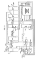
- Fig. 1 shows a distributive computing system wherein the adapter of the present invention may be used.
- the distributive computing system includes a main microprocessor identified by numeral 10.
- a plurality of high speed serial communications links identified by numerals 12, 14 and 16 interconnect the main processor 10 to a plurality of adapters identified by numerals 18, 20 and 22.
- Each adapter in turn interconnects an I/O device (not shown) to the high speed data link.
- adapter 22 can be used to connect a printer to the main processor.
- adapter 20 may be used to interconnect a keyboard (KYBD) to the main processor.
- the adapter 18 may be used to attach the video display device to the main processor.
- data is collected by the I/O devices, processed by the respective adapters and is transferred over the serial data link to the main processor. Likewise, data for a particular device is transferred over the data link via the adapter to the respective I/O device.
- Fig. 2 shows a block diagram of the adapter according to the teaching of the present invention.
- the adapter includes a microprocessor unit (MPU) identified by numeral 24.
- the microprocessor unit is the main controller for the adapter.
- the I/O port of the adapter is coupled to the serial I/O link.
- the microprocessor further includes a serializer/deserializer (not shown) which accepts serial data from the serial I/O link, converts it into parallel data and outputs it on MPU data bus 26.
- the microprocessor is programmed to generate and place a control signal called "MPU to Display" on one of its output PINs. In Fig. 2 the signal is generated and is provided at PIN (Pl.l).
- the signal could have been placed on any other output pin.
- the function of this signal is to inform the read/write control circuitry identified by numeral 28, (details to be given later) to generate the necessary control signals that enable data recorded in the storage area identified as MPU RAM 30 to be transferred into the second storage means identified as display or refresh RAM 32.
- the MPU to display signal is supplied over conductor 34 to the read/write control circuitry.
- a signal identified as "Display to MPU" is generated by the microprocessor unit and is outputted at PIN (Pl.2).
- the function of this signal is to inform the read/write control circuitry to generate the appropriate signals which enable data to flow from display RAM 32 into MPU RAM 30.
- the Display to MPU signal is fed over conductor 36 into read/write control circuitry 28.
- MPU 24 also generates and outputs, a write (WR) signal and a read (RD) signal.
- the read and write signals are fed over conductors 40 and 42, respectively, into the read/write control logic circuitry.
- MPU 24 executes a "Read Command" and the selected RAM is placed in the read mode, the other RAM is placed in the write mode and the information which is read out of a particular address from the RAM that is in the read mode is written into the identical address in the RAM that is in the write mode.
- MPU 24 further provides an address latch enable (ALE) signal which is fed over conductor 44 into latch 46.
- ALE address latch enable
- the ALE signal When the ALE signal is active, the low order byte of the address which is generated at port 0 and fed over MPU data bus 46 is latched into latch 46.
- microprocessor unit 24 is an 8051 8-bit microcomputer manufactured by the Intel Corporation. The operation and construction of this microcomputer is described in the Intel descriptive literature and as such details of the microprocessor will not be given here.
- latch 46 includes 8 latches or 8 D-type flip-flops fabricated in a single package by Texas Instruments, Inc., and identified by catalog number 74LS373. The electrical details and characteristics of this latch means are fully described in the literature provided by Texas Instruments and can be consulted for detailed information relative to the operation and structure of these devices.
- the data bus 26 is connected to latch 46, cathode ray tube controller (CRTC) 50, MPU RAM 30, and transceiver (XCVR) 52.
- the CRT controller 50 provides the interface between the MPU 24 and a raster-scan CRT display. This is an off-the-shelf device and details of the construction and electrical circuitry will not be given here. Suffice it to say that in the preferred embodiment of this invention the MC6845 CRT controller manufactured by Motorola was used. Details of this CRT controller can be obtained from the Motorola literature.
- the CRTC address bus (57) is connected to multiplexor (MVX) 54. Also, a character slice address bus (56) is fed to character generator ROM (Read Only Memory) 58.
- the function of the signal on bus 56 is to provide the address at the particular horizontal slice of the character to be displayed to the character generator ROM (58).
- the combination of the character slice address generated by CRTC (50) and the character itself generated by display RAM (32) provide to the character generator ROM (58) an address that points to the particular slice of a particular character.
- This slice output from character generator ROM (58) is applied to shift register (66) which converts it to a serial data stream (video, 67) which is used to turn the beam on and off on a RASTER scan CRT display.
- Clock pulses are generated by clock 60 and are fed over conductor 62 to the CRTC 50 and over conductor 64 to shift register 66.
- the MPU address bus 48 is coupled to the display RAM address bus 68 by multiplexor means 54.
- a signal called “Select” and identified by numeral 100 is fed from read/write control logic circuit 28 into the multiplexer 54.
- the function of multiplexor 54 is to select which address bus is applied to display RAM address bus 68.
- the "select" signal (100) is used to determine which source the multiplexor (54) uses to apply addresses from. In one state, the CRTC address bus (57) is selected, while in the other state the MPU address bus (48) is selected.
- Display RAM address bus 68 connects the display RAM 32 to the multiplexor 54. Also, display RAM data bus 70 couples the display RAM 32 to the character generator ROM 58. Transceiver 52 couples the display RAM data bus 68 into the MPU data bus 26. The transceiver 52 is an off-the-shelf device whose function is to allow asynchronous two-way communications between data buses. This device allows data to flow from the display RAM data bus 70 to the MPU data bus 26 and vice versa. In the preferred embodiment of this invention the 74LS245 transceiver manufactured by Texas Instruments was used.
- control signals that enable the above components so that data flows from display RAM 32 into MPU RAM 30 or from MPU RAM 30 into display-RAM 32 is generated by read/write control logic circuit means 28.
- the control logic circuit is activated by a read, write, MPU to display or display to MPU control signals which are generated by MPU 24 and are fed over conductors 42, 40, 34 and 38, respectively, into the read/write control logic circuit 28.
- the read/write control logic circuit means 28 processes the input signals and generates therefrom a display RAM read (OE) signal, a display RAM Write (WE) signal, an MPU RAM Read (OE) signal, an MPU RAM Write (WE) signal, an XCVR enable signal, a XCVR direction signal and a MUX select signal. Each of these signals is fed over appropriate conductors into XCVR 52, MPU RAM 30, display RAM 32 and MUX 54.
- the MUX select signal is generated on conductor 106; the XCVR direction signal on conductor 108; the XCVR enable signal on conductor 110; the MPU RAM OE signal on conductor 112; the MPU RAM WE signal on conductor 114; the display RAM OE signal on conductor 116 and the display RAM WE signal on conductor 118.
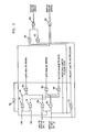
- Fig. 3 shows the details of read/write control logic circuit means 28.
- the circuit includes a pair of NAND logic circuit blocks identified by numerals 70 and 72, respectively.
- the read signal from the MPU is fed into one input of NAND block 70 while the signal on the other input to NAND block 70 is the output from NOR block 74 via inverter 76.
- the output from NAND block 70 is fed over conductor 78 into NOR block 80.
- the other input to NOR block 80 is fed from NAND block 84, NAND block 84 is a two-way NAND block which is supplied by the read signal and the MPU to display signal from the MPU.
- NAND block 86 is a two-way NAND block and is supplied with the read signal and the display to MPU signal.
- the output from NOR block 80 is a read signal which is identified as MPU RAM OE.
- the write signal to the MPU RAM (MPU RAM WE) is outputted from NOR block 82.
- the input to NOR block 82 is formed from the output of NAND blocks 72 and 86, respectively.
- NAND block 72 is a two-way NAND block which is supplied by the write signal and the output from NOR block 74 via inverter 76.
- the output enable to XCVR signal is generated from NAND block 88.
- the output from NAND blocks 84 and 86, respectively, are fed into NAND block 88.
- the Select Line to multiplexors signal is generated from NOR block 74.
- the input signals to NOR block 74 are comprised of the Display to MPU and the MPU to Display signals.
- the read signal to the RAM identified as (Display RAM OE) (Read) is generated by NAND blocks 90, 92 and NOR block 94.
- the inputs to NAND blocks 90 and 92 are read signal, the Display to MPU signal, and the MPU to display signal.
- the output from NAND blocks 90 and 92 are fed over respective conductors to NOR block 94.
- the write signal to the display RAM identified in Fig. 3 as Display RAM WE (Write) is outputted from NAND block 96.
- the input to NAND block 96 is supplied from the display to MPU signal and the read signal.
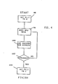
- Fig. 4 shows a flow chart for programming the 8051 MPU so that a copy of the information in the MPU RAM can be transferred to the display RAM. It should be noted that for a copy of the display RAM to be transferred to the MPU RAM Pl.2 (Fig. 2) should be set and cleared rather than Pl.l. Also, the input conditions are that the data pointer (DPTR) should be set to the starting address of the RAM to be copied and that register RO (in the MPU) contains the number of bytes to be copied.
- DPTR data pointer
- register RO in the MPU
- block 96 defines the first step in the process to control the processor.
- the first is a functional one that requires the output PIN Pl.l (Fig. 2) to be set to a logical "0.”
- the program descends into block 98 where an MPU read command is executed by the processor.
- the program then descends into block 100 where the address pointer and a counter are incremented.
- the program then descends into block 102 where it determines if the full range of addresses is copied. If the full range of address is copied, the program descends into block 104 where it sets Pl.l to a logical "1" and exits the routine.
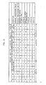
- Fig. 5 shows the read/write logic truth table for the logic circuit of Fig. 3.
- the first four columns of the table represent the input signal which is outputted from the MPU 24, Fig. 1, into read/write control logic circuit 28.
- the next seven columns represent the output signals which are generated from the read/write control logic circuit 28 as a result of the input signals.
- the last column in the table represents the function which is provided.
- the symbols in each column represent the state of the named signal.
- the MPU OE signal On the output, the MPU OE signal is down, the MPU write signal is a logical 1, the display read signal is a logical 0, the display write signal is a logical 1, and so forth.
- the table is self-explanatory and as such each function will not be described. It should be noted that in reading this table the symbol indicates a low level active pulse. This concludes the detailed description.
- Data busses of the display RAM and the MPU RAM 30 are connected via transceiver 52. Each address that the processor reads from MPU RAM 30 is written into the display RAM 32 at the same location. By going through a sequence of addresses during non-display periods, data is updated in the display RAM 32. This process works in reverse as well by putting the processor RAM in write mode while reading from display RAM 32. As a result, this adapter takes a serial message of indeterminate length and puts it into the display RAM.
Landscapes
- Engineering & Computer Science (AREA)
- Theoretical Computer Science (AREA)
- Physics & Mathematics (AREA)
- General Physics & Mathematics (AREA)
- Human Computer Interaction (AREA)
- General Engineering & Computer Science (AREA)
- Computer Hardware Design (AREA)
- Controls And Circuits For Display Device (AREA)
- Communication Control (AREA)
- Digital Computer Display Output (AREA)
- Computer And Data Communications (AREA)
Abstract
Description
- The present invention relates to interface circuit arrangements in general and more particularly to interface circuit arrangements that connect I/O devices to data processing systems.
- Either a parallel communications network or a serial communications network has been used to provide communication between a data processing system and I/O terminals. Such I/O terminals may include displays, keyboards, scanners, etc. Most data processing systems and related I/O terminals differ in their designs and/or operation. In order to provide a somewhat standardized communications network an adapter is often used to capture and/or deliver data and other information to or from the communications network.
- In the case of a parallel communications network the adapter is attached to a parallel data bus. When the I/O terminal is a display unit, data is read out of or written into a display random access memory (RAM) during a non-refreshed period (typically during horizontal and/or vertical retrace). Since this is an asynchronous event, relative to the bus timing, a read/write (R/W) control logic performs the synchronization necessary to get data into or out of the RAM during a non-display period. Although this technique works well for its intended purpose, it has several drawbacks including the fact that a multi-wire data bus is needed. Such multi-wire data buses are usually costly. In addition, the main engine or system microprocessor which places data on the multiplexor bus must wait for the adapter or be interrupted by it.
- In the case of a serial communications network, a data format conversion circuit associated with each terminal is located at the parallel data processing system for converting parallel data to serial data and transmitting the serial data on a pair of lines running to each terminal. In most systems, two additional lines are used for carrying serial data from the terminals to the data processing system. The serial data is delivered to another data format conversion circuit which converts the serial data into parallel data. In this arrangement, at least two data format conversion circuits are needed at the central data processing system.
- In an improvement aimed at reducing the component count of the prior art circuitry, U.S. Patent 4,377,848 describes a data distribution interface in which a single data format conversion circuitry is used at the data processing system to effectuate parallel to serial conversion and vice versa.
- It is therefore the general object of the present invention to provide a more efficient interface circuitry for attaching an I/O device to a serial communications link.
- The interface circuit includes a microprocessor having its own serializer/deserializer. Data is received from a host processor, via the serial communications link, and is placed into the working storage area of the microprocessor. Once the serial message has been received, the local processor manipulates the data and places it at the same address that it would be in if it were in the refresh memory of a display. At a preassigned time (preferably the vertical retrace time) the address bus of the microprocessor is switched into the address bus of the refresh memory. The microprocessor then executes a "read" instruction on its own working storage area but at an address which is identical to the address in refresh memory which is to be updated by data stored in the microprocessor working storage area. The processor's working storage area is placed in a "read" mode while the refresh memory is placed in the "write" mode. The data bus of the processor is switched into the data bus of the refresh memory. As a result, the data which is read from the processor working storage area is transferred to the refresh RAM to update the contents therein. Similarly, a single "read command" can be used for transferring data from the refresh RAM into the microprocessor RAM.
- Fig. 1 shows a block diagram of a computing system embodying the teachings of the present invention.
- Fig. 2 shows a block diagram of the invention according to the teachings of the present invention.
- Fig. 3 shows the details for a read/write control circuitry.
- Fig. 4 shows a flow chart for programming the adapter's microprocessor.
- Fig. 5 shows a truth table for the read/write control circuitry.
- Fig. 1 shows a distributive computing system wherein the adapter of the present invention may be used. The distributive computing system includes a main microprocessor identified by
numeral 10. A plurality of high speed serial communications links identified bynumerals main processor 10 to a plurality of adapters identified bynumerals adapter 22 can be used to connect a printer to the main processor. Likewise,adapter 20 may be used to interconnect a keyboard (KYBD) to the main processor. Finally, theadapter 18 may be used to attach the video display device to the main processor. - In a typical installation, such as may be found in a store, data is collected by the I/O devices, processed by the respective adapters and is transferred over the serial data link to the main processor. Likewise, data for a particular device is transferred over the data link via the adapter to the respective I/O device.
- Although the present invention may be used in other environments, it works well in attaching a video display device to the main processor of Fig. 1 and as such will be described in that environment. However, this should not be construed as a limitation on the scope of the present invention since it is within the skill of one skilled in the art to make minor changes and/or adjustments to the below-described adapter without departing from the scope of the present invention.
- Fig. 2 shows a block diagram of the adapter according to the teaching of the present invention. The adapter includes a microprocessor unit (MPU) identified by
numeral 24. The microprocessor unit is the main controller for the adapter. To this end, the I/O port of the adapter is coupled to the serial I/O link. The microprocessor further includes a serializer/deserializer (not shown) which accepts serial data from the serial I/O link, converts it into parallel data and outputs it onMPU data bus 26. Furthermore, the microprocessor is programmed to generate and place a control signal called "MPU to Display" on one of its output PINs. In Fig. 2 the signal is generated and is provided at PIN (Pl.l). Of course, the signal could have been placed on any other output pin. As will be explained subsequently, the function of this signal is to inform the read/write control circuitry identified bynumeral 28, (details to be given later) to generate the necessary control signals that enable data recorded in the storage area identified as MPU RAM 30 to be transferred into the second storage means identified as display or refresh RAM 32. The MPU to display signal is supplied overconductor 34 to the read/write control circuitry. Similarly, a signal identified as "Display to MPU" is generated by the microprocessor unit and is outputted at PIN (Pl.2). The function of this signal is to inform the read/write control circuitry to generate the appropriate signals which enable data to flow from display RAM 32 into MPU RAM 30. The Display to MPU signal is fed over conductor 36 into read/writecontrol circuitry 28. MPU 24 also generates and outputs, a write (WR) signal and a read (RD) signal. The read and write signals are fed overconductors - MPU 24 further provides an address latch enable (ALE) signal which is fed over
conductor 44 into latch 46. When the ALE signal is active, the low order byte of the address which is generated atport 0 and fed over MPU data bus 46 is latched into latch 46. It should be noted that although the control signals are shown in Fig. 2 to be taken from named ports of the microprocessor, this should not be construed as a limitation on the scope of the present invention since the ports are interchangeable and other ports can be used to provide the signals which are used to control this adapter. Also, any collection of logic, including, but not limited to, any off-the-shelf microprocessor which is manufactured as a device controller may be used to replaceMPU 24. In the preferred embodiment of this invention,microprocessor unit 24 is an 8051 8-bit microcomputer manufactured by the Intel Corporation. The operation and construction of this microcomputer is described in the Intel descriptive literature and as such details of the microprocessor will not be given here. Also, latch 46 includes 8 latches or 8 D-type flip-flops fabricated in a single package by Texas Instruments, Inc., and identified by catalog number 74LS373. The electrical details and characteristics of this latch means are fully described in the literature provided by Texas Instruments and can be consulted for detailed information relative to the operation and structure of these devices. - Still referring to Fig. 2, the
data bus 26 is connected to latch 46, cathode ray tube controller (CRTC) 50, MPU RAM 30, and transceiver (XCVR) 52. TheCRT controller 50 provides the interface between theMPU 24 and a raster-scan CRT display. This is an off-the-shelf device and details of the construction and electrical circuitry will not be given here. Suffice it to say that in the preferred embodiment of this invention the MC6845 CRT controller manufactured by Motorola was used. Details of this CRT controller can be obtained from the Motorola literature. The CRTC address bus (57) is connected to multiplexor (MVX) 54. Also, a character slice address bus (56) is fed to character generator ROM (Read Only Memory) 58. The function of the signal onbus 56 is to provide the address at the particular horizontal slice of the character to be displayed to the character generator ROM (58). The combination of the character slice address generated by CRTC (50) and the character itself generated by display RAM (32) provide to the character generator ROM (58) an address that points to the particular slice of a particular character. This slice output from character generator ROM (58) is applied to shift register (66) which converts it to a serial data stream (video, 67) which is used to turn the beam on and off on a RASTER scan CRT display. - Clock pulses are generated by clock 60 and are fed over
conductor 62 to theCRTC 50 and over conductor 64 to shiftregister 66. - Still referring to Fig. 2, the
MPU address bus 48 is coupled to the displayRAM address bus 68 by multiplexor means 54. A signal called "Select" and identified bynumeral 100 is fed from read/writecontrol logic circuit 28 into themultiplexer 54. The function ofmultiplexor 54 is to select which address bus is applied to displayRAM address bus 68. The "select" signal (100) is used to determine which source the multiplexor (54) uses to apply addresses from. In one state, the CRTC address bus (57) is selected, while in the other state the MPU address bus (48) is selected. - In the preferred embodiment of this invention, 3 multiplexor fabricated by Texas Instruments and identified by the manufacturer's number SN74LS157 connected in tandem were used. Of course, other multiplexor configurations may be used without departing from the scope of the present invention.
- Display
RAM address bus 68 connects the display RAM 32 to themultiplexor 54. Also, displayRAM data bus 70 couples the display RAM 32 to the character generator ROM 58.Transceiver 52 couples the displayRAM data bus 68 into theMPU data bus 26. Thetransceiver 52 is an off-the-shelf device whose function is to allow asynchronous two-way communications between data buses. This device allows data to flow from the displayRAM data bus 70 to theMPU data bus 26 and vice versa. In the preferred embodiment of this invention the 74LS245 transceiver manufactured by Texas Instruments was used. - Still referring to Fig. 2, the control signals that enable the above components so that data flows from display RAM 32 into MPU RAM 30 or from MPU RAM 30 into display-RAM 32 is generated by read/write control logic circuit means 28. The control logic circuit is activated by a read, write, MPU to display or display to MPU control signals which are generated by
MPU 24 and are fed overconductors control logic circuit 28. The read/write control logic circuit means 28 processes the input signals and generates therefrom a display RAM read (OE) signal, a display RAM Write (WE) signal, an MPU RAM Read (OE) signal, an MPU RAM Write (WE) signal, an XCVR enable signal, a XCVR direction signal and a MUX select signal. Each of these signals is fed over appropriate conductors intoXCVR 52, MPU RAM 30, display RAM 32 andMUX 54. For example, the MUX select signal is generated onconductor 106; the XCVR direction signal onconductor 108; the XCVR enable signal onconductor 110; the MPU RAM OE signal onconductor 112; the MPU RAM WE signal onconductor 114; the display RAM OE signal onconductor 116 and the display RAM WE signal onconductor 118. - Fig. 3 shows the details of read/write control logic circuit means 28. The circuit includes a pair of NAND logic circuit blocks identified by
numerals NAND block 70 while the signal on the other input toNAND block 70 is the output from NOR block 74 viainverter 76. The output fromNAND block 70 is fed overconductor 78 into NORblock 80. The other input to NOR block 80 is fed fromNAND block 84,NAND block 84 is a two-way NAND block which is supplied by the read signal and the MPU to display signal from the MPU. Likewise,NAND block 86 is a two-way NAND block and is supplied with the read signal and the display to MPU signal. The output from NORblock 80 is a read signal which is identified as MPU RAM OE. The write signal to the MPU RAM (MPU RAM WE) is outputted from NORblock 82. The input to NOR block 82 is formed from the output of NAND blocks 72 and 86, respectively.NAND block 72 is a two-way NAND block which is supplied by the write signal and the output from NOR block 74 viainverter 76. - The output enable to XCVR signal is generated from
NAND block 88. The output from NAND blocks 84 and 86, respectively, are fed intoNAND block 88. The Select Line to multiplexors signal is generated from NORblock 74. The input signals to NOR block 74 are comprised of the Display to MPU and the MPU to Display signals. - The read signal to the RAM identified as (Display RAM OE) (Read) is generated by NAND blocks 90, 92 and NOR block 94. The inputs to NAND blocks 90 and 92 are read signal, the Display to MPU signal, and the MPU to display signal. The output from NAND blocks 90 and 92 are fed over respective conductors to NOR block 94.
- Finally, the write signal to the display RAM identified in Fig. 3 as Display RAM WE (Write) is outputted from
NAND block 96. The input toNAND block 96 is supplied from the display to MPU signal and the read signal. - Fig. 4 shows a flow chart for programming the 8051 MPU so that a copy of the information in the MPU RAM can be transferred to the display RAM. It should be noted that for a copy of the display RAM to be transferred to the MPU RAM Pl.2 (Fig. 2) should be set and cleared rather than Pl.l. Also, the input conditions are that the data pointer (DPTR) should be set to the starting address of the RAM to be copied and that register RO (in the MPU) contains the number of bytes to be copied.
- Still referring to Fig. 4, block 96 defines the first step in the process to control the processor. The first is a functional one that requires the output PIN Pl.l (Fig. 2) to be set to a logical "0." From
block 96 the program descends intoblock 98 where an MPU read command is executed by the processor. The program then descends intoblock 100 where the address pointer and a counter are incremented. The program then descends intoblock 102 where it determines if the full range of addresses is copied. If the full range of address is copied, the program descends intoblock 104 where it sets Pl.l to a logical "1" and exits the routine. However, inblock 102, if the full range of addresses was not copied, then the program enters into a loop and continues copying and updating the address counter until the full range of addresses is copied from one buffer into the next. As stated previously, the same routine can be used to effectuate the data transfer from the display buffer into the MPU buffer. In that event, the PIN P1.2 (Display to MPU) is set instead of Pl.l (MPU to Display). - Fig. 5 shows the read/write logic truth table for the logic circuit of Fig. 3. The first four columns of the table represent the input signal which is outputted from the
MPU 24, Fig. 1, into read/writecontrol logic circuit 28. The next seven columns represent the output signals which are generated from the read/writecontrol logic circuit 28 as a result of the input signals. Finally, the last column in the table represents the function which is provided. The symbols in each column represent the state of the named signal. Thus, in order to do a normal processor read the signal on the read line into the logic circuit means has to be in a down state. The write line has to be up, the MPU to display has to be a logical 1, and the display to MPU has to be a logical 1. On the output, the MPU OE signal is down, the MPU write signal is a logical 1, the display read signal is a logical 0, the display write signal is a logical 1, and so forth. As is evident from this first example, the table is self-explanatory and as such each function will not be described. It should be noted that in reading this table the symbol indicates a low level active pulse. This concludes the detailed description. - Having described the detailed configuration of the adapter, its operation will now be given. In operation, when data is received from the host processor (Fig. 1), the data is placed into MPU RAM 30, Fig. 2. With the data in MPU RAM 30,
MPU 24 manipulates the data at the same address that the data would be in if it were in display RAM 32. Stated another way, common or identical addresses in MPU RAM 30 and display RAM 32 are used to store identical data. At vertical retrace time the processor address bus is switched by multiplexor means 54 into the displayRAM address bus 68. The processor then executes a read instruction at the addresses in display RAM 32 that are to be updated by data contained in MPU RAM 30. The processor memory is placed in read mode while the display RAM 32 is placed in write mode. Data busses of the display RAM and the MPU RAM 30 are connected viatransceiver 52. Each address that the processor reads from MPU RAM 30 is written into the display RAM 32 at the same location. By going through a sequence of addresses during non-display periods, data is updated in the display RAM 32. This process works in reverse as well by putting the processor RAM in write mode while reading from display RAM 32. As a result, this adapter takes a serial message of indeterminate length and puts it into the display RAM.
Claims (6)
Applications Claiming Priority (2)
| Application Number | Priority Date | Filing Date | Title |
|---|---|---|---|
| US67251284A | 1984-11-19 | 1984-11-19 | |
| US672512 | 1984-11-19 |
Publications (3)
| Publication Number | Publication Date |
|---|---|
| EP0182097A2 true EP0182097A2 (en) | 1986-05-28 |
| EP0182097A3 EP0182097A3 (en) | 1990-03-14 |
| EP0182097B1 EP0182097B1 (en) | 1993-02-03 |
Family
ID=24698864
Family Applications (1)
| Application Number | Title | Priority Date | Filing Date |
|---|---|---|---|
| EP85113094A Expired - Lifetime EP0182097B1 (en) | 1984-11-19 | 1985-10-15 | Serially attached video adapter |
Country Status (4)
| Country | Link |
|---|---|
| US (1) | US4959773A (en) |
| EP (1) | EP0182097B1 (en) |
| JP (1) | JPS61125665A (en) |
| DE (1) | DE3587062T2 (en) |
Cited By (1)
| Publication number | Priority date | Publication date | Assignee | Title |
|---|---|---|---|---|
| EP0501901A2 (en) * | 1991-02-28 | 1992-09-02 | International Business Machines Corporation | Display station controller |
Families Citing this family (4)
| Publication number | Priority date | Publication date | Assignee | Title |
|---|---|---|---|---|
| US5257393A (en) * | 1989-04-19 | 1993-10-26 | Jrm Consultants, Inc. | Serially controlled programmable test network |
| AU624274B2 (en) * | 1989-11-20 | 1992-06-04 | Digital Equipment Corporation | Data format for packets of information |
| US5613156A (en) | 1994-09-27 | 1997-03-18 | Eastman Kodak Company | Imaging system with 1-N Parallel channels, each channel has a programmable amplifier and ADC with serial controller linking and controlling the amplifiers and ADCs |
| JP3636148B2 (en) * | 2002-03-07 | 2005-04-06 | セイコーエプソン株式会社 | Display driver, electro-optical device, and display driver parameter setting method |
Citations (3)
| Publication number | Priority date | Publication date | Assignee | Title |
|---|---|---|---|---|
| EP0067302A2 (en) * | 1981-06-16 | 1982-12-22 | International Business Machines Corporation | Display updating device in a data communication system |
| EP0105725A2 (en) * | 1982-09-29 | 1984-04-18 | Fanuc Ltd. | Display unit |
| JPS60117327A (en) * | 1983-11-30 | 1985-06-24 | Fuji Xerox Co Ltd | Display device |
Family Cites Families (14)
| Publication number | Priority date | Publication date | Assignee | Title |
|---|---|---|---|---|
| US3774161A (en) * | 1971-05-14 | 1973-11-20 | Raytheon Co | Visual display system |
| US4023142A (en) * | 1975-04-14 | 1977-05-10 | International Business Machines Corporation | Common diagnostic bus for computer systems to enable testing concurrently with normal system operation |
| US4075695A (en) * | 1976-06-01 | 1978-02-21 | Raytheon Company | Display processor system |
| US4232376A (en) * | 1979-03-15 | 1980-11-04 | Rca Corporation | Raster display refresh system |
| US4513390A (en) * | 1979-06-08 | 1985-04-23 | Planning Research Corporation | System for digital transmission and synthesis of integrated data |
| US4322812A (en) * | 1979-10-16 | 1982-03-30 | Burroughs Corporation | Digital data processor providing for monitoring, changing and loading of RAM instruction data |
| US4398265A (en) * | 1980-09-15 | 1983-08-09 | Motorola, Inc. | Keyboard and display interface adapter architecture |
| JPS5890866A (en) * | 1981-11-26 | 1983-05-30 | Hitachi Ltd | Transmitter for picture information |
| US4575803A (en) * | 1981-12-30 | 1986-03-11 | Semco Instruments, Inc. | Engine monitor and recorder |
| US4559620A (en) * | 1982-09-14 | 1985-12-17 | Mobil Oil Corporation | Mass memory system addressing circuit |
| US4574358A (en) * | 1982-09-14 | 1986-03-04 | Mobil Oil Corporation | Monitor display control |
| US4573115A (en) * | 1983-10-28 | 1986-02-25 | Standard Oil Company (Indiana) | Supervisory control system for remotely monitoring and controlling at least one operational device |
| US4608688A (en) * | 1983-12-27 | 1986-08-26 | At&T Bell Laboratories | Processing system tolerant of loss of access to secondary storage |
| US4656596A (en) * | 1984-07-23 | 1987-04-07 | Texas Instruments Incorporated | Video memory controller |
-
1985
- 1985-08-14 JP JP60177790A patent/JPS61125665A/en active Granted
- 1985-10-15 EP EP85113094A patent/EP0182097B1/en not_active Expired - Lifetime
- 1985-10-15 DE DE8585113094T patent/DE3587062T2/en not_active Expired - Fee Related
-
1988
- 1988-01-07 US US07/143,283 patent/US4959773A/en not_active Expired - Fee Related
Patent Citations (3)
| Publication number | Priority date | Publication date | Assignee | Title |
|---|---|---|---|---|
| EP0067302A2 (en) * | 1981-06-16 | 1982-12-22 | International Business Machines Corporation | Display updating device in a data communication system |
| EP0105725A2 (en) * | 1982-09-29 | 1984-04-18 | Fanuc Ltd. | Display unit |
| JPS60117327A (en) * | 1983-11-30 | 1985-06-24 | Fuji Xerox Co Ltd | Display device |
Non-Patent Citations (1)
| Title |
|---|
| PATENT ABSTRACTS OF JAPAN, vol. 9, no. 273, 30th October 1985; & JP-A-60 117 327 (FUJI XEROX K.K.) 24-06-1985 * |
Cited By (3)
| Publication number | Priority date | Publication date | Assignee | Title |
|---|---|---|---|---|
| EP0501901A2 (en) * | 1991-02-28 | 1992-09-02 | International Business Machines Corporation | Display station controller |
| EP0501901A3 (en) * | 1991-02-28 | 1993-06-16 | International Business Machines Corporation | Display station controller |
| US5485570A (en) * | 1991-02-28 | 1996-01-16 | International Business Machines Corporation | Display station controller |
Also Published As
| Publication number | Publication date |
|---|---|
| DE3587062D1 (en) | 1993-03-18 |
| EP0182097A3 (en) | 1990-03-14 |
| US4959773A (en) | 1990-09-25 |
| DE3587062T2 (en) | 1993-08-12 |
| JPS61125665A (en) | 1986-06-13 |
| JPH0419569B2 (en) | 1992-03-30 |
| EP0182097B1 (en) | 1993-02-03 |
Similar Documents
| Publication | Publication Date | Title |
|---|---|---|
| US4195344A (en) | Computer system with a configuration monitor | |
| EP0522764B1 (en) | Multiplexing scheme for modem control signals | |
| US5250940A (en) | Multi-mode home terminal system that utilizes a single embedded general purpose/DSP processor and a single random access memory | |
| EP0332361B1 (en) | Method and apparatus for logic simulation | |
| KR930003709B1 (en) | Data transmission controller and its method | |
| EP0079468B1 (en) | Direct memory access method for use with a multiplexed data bus | |
| EP0221509B1 (en) | Apparatus providing improved diagnosability | |
| EP0177616A1 (en) | System for selecting address in input/output board | |
| US4525804A (en) | Interface apparatus for host computer and graphics terminal | |
| US5465106A (en) | Generic driver interface card | |
| US4959773A (en) | Adapter for attaching I/O devices to I/O communications with alternating read and write modes link | |
| EP0331487B1 (en) | Data transfer control system | |
| US3986170A (en) | Modular control system design with microprocessors | |
| US4787025A (en) | Remote fan out facility for data terminals | |
| US6851001B1 (en) | Address remapping for a bus | |
| US5148516A (en) | Efficient computer terminal system utilizing a single slave processor | |
| US4625203A (en) | Arrangement for providing data signals for a data display system | |
| US4940971A (en) | Bit map display apparatus for performing an interruption display among planes at high speed | |
| US4583167A (en) | Procedure and apparatus for conveying external and output data to a processor system | |
| US6088372A (en) | Time division multiplexing system for digital exchange | |
| GB2080582A (en) | Procedure and apparatus for conveying external input and output data to a processor system | |
| JPS5922585Y2 (en) | Display device control circuit | |
| EP0273637A2 (en) | Bit pattern conversion system | |
| EP0260793A2 (en) | Bidirectional data bus | |
| SU1591028A1 (en) | Device for interfacing subscribers with computer |
Legal Events
| Date | Code | Title | Description |
|---|---|---|---|
| PUAI | Public reference made under article 153(3) epc to a published international application that has entered the european phase |
Free format text: ORIGINAL CODE: 0009012 |
|
| AK | Designated contracting states |
Kind code of ref document: A2 Designated state(s): DE FR GB |
|
| 17P | Request for examination filed |
Effective date: 19860919 |
|
| PUAL | Search report despatched |
Free format text: ORIGINAL CODE: 0009013 |
|
| AK | Designated contracting states |
Kind code of ref document: A3 Designated state(s): DE FR GB |
|
| 17Q | First examination report despatched |
Effective date: 19910912 |
|
| GRAA | (expected) grant |
Free format text: ORIGINAL CODE: 0009210 |
|
| AK | Designated contracting states |
Kind code of ref document: B1 Designated state(s): DE FR GB |
|
| REF | Corresponds to: |
Ref document number: 3587062 Country of ref document: DE Date of ref document: 19930318 |
|
| ET | Fr: translation filed | ||
| PG25 | Lapsed in a contracting state [announced via postgrant information from national office to epo] |
Ref country code: GB Effective date: 19931015 |
|
| PLBE | No opposition filed within time limit |
Free format text: ORIGINAL CODE: 0009261 |
|
| STAA | Information on the status of an ep patent application or granted ep patent |
Free format text: STATUS: NO OPPOSITION FILED WITHIN TIME LIMIT |
|
| 26N | No opposition filed | ||
| GBPC | Gb: european patent ceased through non-payment of renewal fee |
Effective date: 19931015 |
|
| PG25 | Lapsed in a contracting state [announced via postgrant information from national office to epo] |
Ref country code: FR Effective date: 19940630 |
|
| PG25 | Lapsed in a contracting state [announced via postgrant information from national office to epo] |
Ref country code: DE Effective date: 19940701 |
|
| REG | Reference to a national code |
Ref country code: FR Ref legal event code: ST |