EP0180476A2 - Microprogramme sequence controller - Google Patents
Microprogramme sequence controller Download PDFInfo
- Publication number
- EP0180476A2 EP0180476A2 EP85307899A EP85307899A EP0180476A2 EP 0180476 A2 EP0180476 A2 EP 0180476A2 EP 85307899 A EP85307899 A EP 85307899A EP 85307899 A EP85307899 A EP 85307899A EP 0180476 A2 EP0180476 A2 EP 0180476A2
- Authority
- EP
- European Patent Office
- Prior art keywords
- address
- interrupt
- trap
- instruction
- output
- Prior art date
- Legal status (The legal status is an assumption and is not a legal conclusion. Google has not performed a legal analysis and makes no representation as to the accuracy of the status listed.)
- Granted
Links
- 230000002457 bidirectional effect Effects 0.000 claims description 36
- 238000004891 communication Methods 0.000 claims description 15
- 238000000034 method Methods 0.000 claims description 13
- 230000004044 response Effects 0.000 claims description 11
- 230000008569 process Effects 0.000 claims description 4
- 230000008878 coupling Effects 0.000 claims 6
- 238000010168 coupling process Methods 0.000 claims 6
- 238000005859 coupling reaction Methods 0.000 claims 6
- 230000002401 inhibitory effect Effects 0.000 claims 5
- 230000002427 irreversible effect Effects 0.000 abstract description 2
- 206010000210 abortion Diseases 0.000 abstract 1
- 238000012545 processing Methods 0.000 description 13
- 238000012360 testing method Methods 0.000 description 6
- 230000002093 peripheral effect Effects 0.000 description 4
- 238000010586 diagram Methods 0.000 description 3
- 230000000694 effects Effects 0.000 description 3
- 230000006870 function Effects 0.000 description 3
- 238000013507 mapping Methods 0.000 description 3
- 230000009471 action Effects 0.000 description 2
- 230000008901 benefit Effects 0.000 description 2
- 230000008859 change Effects 0.000 description 2
- 238000001514 detection method Methods 0.000 description 2
- 238000013459 approach Methods 0.000 description 1
- 238000003491 array Methods 0.000 description 1
- 230000003139 buffering effect Effects 0.000 description 1
- 239000013256 coordination polymer Substances 0.000 description 1
- 230000003247 decreasing effect Effects 0.000 description 1
- 238000013461 design Methods 0.000 description 1
- 230000007257 malfunction Effects 0.000 description 1
- 238000004519 manufacturing process Methods 0.000 description 1
- 230000011664 signaling Effects 0.000 description 1
- 238000006467 substitution reaction Methods 0.000 description 1
- 230000001360 synchronised effect Effects 0.000 description 1
Images

Classifications
-
- G—PHYSICS
- G06—COMPUTING; CALCULATING OR COUNTING
- G06F—ELECTRIC DIGITAL DATA PROCESSING
- G06F9/00—Arrangements for program control, e.g. control units
- G06F9/06—Arrangements for program control, e.g. control units using stored programs, i.e. using an internal store of processing equipment to receive or retain programs
- G06F9/22—Microcontrol or microprogram arrangements
- G06F9/26—Address formation of the next micro-instruction ; Microprogram storage or retrieval arrangements
- G06F9/262—Arrangements for next microinstruction selection
- G06F9/268—Microinstruction selection not based on processing results, e.g. interrupt, patch, first cycle store, diagnostic programs
-
- G—PHYSICS
- G06—COMPUTING; CALCULATING OR COUNTING
- G06F—ELECTRIC DIGITAL DATA PROCESSING
- G06F13/00—Interconnection of, or transfer of information or other signals between, memories, input/output devices or central processing units
- G06F13/14—Handling requests for interconnection or transfer
- G06F13/20—Handling requests for interconnection or transfer for access to input/output bus
- G06F13/24—Handling requests for interconnection or transfer for access to input/output bus using interrupt
Abstract
Description
- This invention relates generally to a microprogram sequence controller for controlling the sequence of execution of microinstructions stored in a microprogram memory, and preferably to a microprogram sequence controller having on-chip circuitry which affords user-selectrable operation of the controller in either an interrupt-mode or a trap-mode.
- Reference may be made to our copending European Patent Application 85 303224.1 (published as number ).
- Typically, microprogrammed systems are constructed from a variety of very large scale integrated circuit (VLSI) chips used as building blocks in an architecture which can be divided into two subsections: a control section that supervises the order and decoding of instructions to be executed, and a data processing section which performs the operations called for by the instructions on the data. The control section normally includes a microprogram sequence controller that issues microprogram addresses, and a microprogram memory which contains microinstructions.
- Each microinstruction includes a plurality of bits to control the element with the data processing section. In addition, the microinstruction may have a peripheral control portion comprising a plurality of bits communicated to an "intelligent" peripheral unit
- so that when called upon to receive or transmit data to the host microprogrammed system, the call requires a minimum of time and control by the host microcomputer. In peripheral controller operation, the microcomputer is often faced with the requirement for the efficient synchronization and response to asynchronous events such as power failure, machine malfunctions, control panel service requests, external timer signals, and input/output device service requests. Handling these asynchronous events, in terms of response time, systems throughput, hardware costs, and memory space required, is a true measure of the performance of the system.
- One approach to handling asynchronous events is to incorporate circuitry that provides a status indicator associated with each possible asynchronous event. The microcomputer system then tests each indicator in sequence and, in effect, "asks" if service is required. This is typically referred to as the "polling" method and is often microprogram software implemented. This polling method, however, consumes time and microprogram memory space. System throughput is decreased, response time increased, and microprogram memory space that could otherwise be used for additional purposes dedicated to handling responses to these asynchronous events.
- Asynchronous events can also be handled via what is termed an "interrupt" technique whereby the event generates a request signal. The microcomputer system, upon receipt of the request signal, may suspend the program it is presently executing, execute an event service routine, then resume execution of the suspended program. This method, at the additional expense of circuitry, is preferred, particularly in high performance operating systems. The microcomputer is not burdened with having to poll all status signals. Rather, a service routine is executed only when requested. Thus, the system is more efficient since response time is faster; and it is this low response time that is sought by the high performance data processing systems of today.
- Yet, there still exists certain problems and disadvantages using the interrupt technique with today's available bipolar microcomputer systems. Presently, additional circuitry is necessary and the sequencer must be programmed to take the time to service the interrupt request circuitry itself. Furthermore, an interrupt technique is usually implemented so that before suspending the program presently executing, the microinstruction being executed at the time the interrupt request signal is received is allowed to be completed. The resulting newly-updated contents of all registers, the program counter, and certain other quantities are saved and then control is transferred to the appropriate interrupt event service routine.
- However, certain asynchronous events are of such a nature that completion of the presently-executing microinstruction will cause irreversible error. For example, if the present microinstruction calls for writing a word to memory across a word boundary in a single cycle. To avoid such error, present microprogram sequence controllers must be specially equipped with a substantial amount of external logic circuitry to implement what is termed a "trap." Attendant to such circuitry is an increased chip count, chip costs, pin interconnection, space requirements, and inter-chip signal propagation delay.
- The present invention is directed to a microprogram sequence controller having circuitry that permits both "interruption" and "trapping" of presently-executing instruction streams. In any given application, the particular method of handling an asynchronous event is readily chosen by the user by applying a particular set of external signals to the controller's terminal pins. The overall controller architecture is structured so that it can be fabricated as a single integrated circuit.
- According to the present invention, a microprogram controller, used as an address sequencer intended for controlling the sequence of execution of microinstructions stored in a microprogram memory, is provided with circuitry that automatically allows the controller to abort execution of the presently-executing microinstruction and branch to a predetermined subroutine in response to a request for asynchronous event handling (hereinafter "trap"). The controller includes circuitry for generating sequential addresses that are applied to the microprogram memory for accessing a sequential set of microinstructions, a program address register that holds the generated address, a random access memory (RAM), a last-in, first-out stack, and interrupt/trap handling logic circuitry.
- When an asynchronous event handling request is received, the interrupt/trap handling logic determines which mode is to be employed to service the request, i.e., by interrupting the present instruction stream following execution of the presently-executing microinstruction, or by trapping the presently-executing microinstruction stream and aborting the presently-executing microinstruction as selected by external signals. The logic circuitry will store the information presently extant in the controller to allow it to return to the proper point in the presently-executing stream, i.e., either the microinstruction next-following the one interrupted, or the microinstruction executing when it was trapped, after the subroutine has been completed which services the asynchronous event.
- The interrupt/trap handling logic of the present invention can handle any level of nesting of in- terrupts/traps. For a fuller understanding of the nature and advantages of the invention, reference should be had to the ensuing detailed description taken in conjunction with the accompanying drawings.
-
- Fig. 1 illustrates a typical application of the trap handling microprogram sequence controller of the present invention in a microprocessor;
- Figs. 2A and 2B are functional block diagrams of the trap handling microprogram sequence controller of the present invention;
- Fig. 3A is a diagram of the interrupt/trap detect circuit used in the interrupt/trap logic circuit of the invention of Figs. 2A and 2B;
- Fig. 3B is a diagram of the carry-in to incrementer circuit used in the incrementer of the invention of Figs. 2A and 2B.
- Many programmable digital devices today utilize microprogramming. In such devices, a large portion of the device's control is performed utilizing a read-only-memory (ROM) rather than large arrays of gates and flip-flops. This technique frequently reduces the package count in the digital device and provides a highly ordered structure, not present when random logic is used. Moreover, microprogramming makes changes in the device's instruction set very simple to perform, reducing post-production engineering costs for the device substantially.
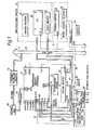
- Fig. 1 illustrates the typical microprocessor system architecture used in a programmable digital device and can be divided into two distinct sections: an instruction acquisition and processing section A on the left and a data acquisition and processing manipulation section B on the right. Section A has, as its heart, the microprogram sequence controller of the present invention, generally designated with the
reference numeral 10. The data acquisition and manipulation section B includes the data processing circuits, generally designated as 12, which includes the working registers 14, the arithmetic logic unit (ALU) 16 and thestatus register 18. The data processing circuits process data acquired frommemory 20 by performing whatever operations are required by the "machine" instruction pointed to by the data acquisition circuits, generally designated as 21, as addressed byprogram counter 22 and accessed via the memory address register 24. Each "machine" instruction is implemented on the microprocessor by a sequence of microinstructions selected by themicroprogram sequence controller 10. - While, for the purposes of discussion, certain of the blocks shown in Fig. 1 are shown explicitly interconnected by designated lines, it is to be understood that data communication between any of the blocks shown can be effected along the
bidirectional data bus 26. Similarly addresses can be communicated between any of the blocks shown, onaddress bus 28. -
Microprogram sequence controller 10 generates addresses that determine the sequence of microinstructions that ultimately issue from themicroprogram memory 30. The addresses generated by themicroprogram sequence controller 10 are conducted from DATA OUT terminals ofcontroller 10 on a "Y"address bus 32 to the address circuits (not shown) of themicroprogram memory 30. With the application of such microinstruction addresses, themicroprogram memory 30 will issue, on the microinstruction bus 34, microinstructions, usually of a word length on the order of 32 or more bits. - The microinstruction bus 34 conducts the microinstructions to the data inputs of a pipeline register 36, which accepts and temporarily holds the microinstruction. While the microinstruction is contained in pipeline register 36, output lines of the register go out to the various system elements, including a portion of the microinstruction which is returned to the sequencer controller to determine the address of the next microinstruction to be executed. That next address is computed by the
microprogram sequence controller 10, conducted to themicroprogram memory 30 via the "Y"address bus 32, and the next microinstruction sits at the input of the pipeline register 36. - Those portions of the microinstruction that are returned to the
microprogram sequence controller 10 include a 6-bit controller instruction word, conducted on acontroller instruction bus 38 and a multi-bit data word that is conducted on acontroller data bus 40 to the data bus inputs of thesequence controller 10. - other portions of the microinstruction are control signals which are conveyed to the data processing circuits 12 along
processor instruction bus 42. These signals cause data to be transferred frommemory 20 to the working register 14 and then processed by thearithmetic logic unit 16 and the result transferred tomemory 20. During the processing of the data the processor may set certain bits instatus register 18. The processor device can communicate this information to themicroprogram sequence controller 10. For example, thestatus register 18 signals may be placed on the condition test (CT) output of the data processing circuits includes circuitry that can multiplex a plurality of condition test signals to the CT output. A detailed description of data processing circuits providing the functions herein described is supplied in "Bit-Slice Microprocessor Design" by John Mick and Jim Brick, McGraw-Hill, 1980 ISBN 0-07-041781-4. - The test signals appearing at the CT output of the data processing circuits 12 are applied to the TEST inputs of the
microprogram controller 10, via the status signal lines 44, where, under control of the select inputs SO-S3, they are used to conditionally modify the address that will be presented to themicroprogram memory 30. - Microinstruction "branch" addresses can be obtained from any one of five sources: first, from the
controller data bus 40 to the DATA_IN inputs of the microprogram sequence controller, where it is used for microprogram addresses. A second possible source of microinstruction addresses is from a mapping read-only-memory (ROM) 50 which is connected via amicroinstruction register 51 to the AUX_DATA_IN inputs of themicroprogram sequence controller 10. These addresses are utilized by certain microinstructions as an alternative to the addresses on the DATA_IN inputs. Themapping ROM 50 typically contains the starting microroutine "branch" address and is itself addressed by the output of theinstruction register 52. Theinstruction register 52, in turn, is provided with a "machine instruction" frommemory 20 under the direction ofprogram counter 22. The machine instruction is performed by executing several of the microinstructions (stored in the microprogram memory 30) in sequence. - The so-called four-bit "multiway" inputs M0, Ml, M2 and M3 to
microprogram sequence controller 10 are a third source of microinstruction branch addresses whereby certain microinstructions permit substitution of one of the four-bit patterns present at M0, Ml, M2 or M3 for the least significant four bits at the DATA IN inputs depending on the two least significant bit values on the DATA IN inputs. - The fourth and fifth sources of microinstruction branch addresses are from registers internal to the
controller 10; a return or loop address from the top of a stack register; or the next sequential address from the microprogram counter register. - The
microprogram sequence controller 10 has an internal multiplexer which, under the direction of microinstructions, controls the selection of the particular one of the five sources of branch addresses. - In a typical application of the microprogram sequence controller,
circuitry 54 for servicing asynchronous event handling requests would be included. For example, as shown in Fig. 1, an interrupt/trap controller 56 and in interrupt/trap vector PROM (IVP) 58. The interrupt/trap controller 56 would receive at its inputs (II1, II2, ..., IIn), via corresponding signal lines 60, interrupt or trap signals from individual peripheral units, requesting some type of servicing (i.e., data transfers, reading switches, etc.). When an interrupt or trap signal is received at one of its II1-IIn inputs, the interrupt/trap controller 56 issues interrupt or trap request signals from its interrupt/trap (INT/TRAP) output, which are conducted to a set of interrupt/trap (INTR/TRP) inputs of themicroprogram controller 10 via signal lines 61. As will be seen, the signals received by themicroprogram sequence controller 10 at its INTR/TRP inputs may cause it to initiate a storage routine to store information presently contained in various registers of thecontroller 10 to enable it to return to the present microinstruction sequence at the proper place. - Following receipt of an accepted asynchronous event handling request,
controller 10 generates an acknowledge interrupt/trap signal at output INTA which is sent vialine 62 toIVP 58 and interrupt/trap controller 56, which formulates a multibit word identifying the particular unit requesting servicing. The formulated word is conducted on the signal lines 64 to theIVP 58. Each memory location of theIVP 58 contains an address of each sequence of microinstructions contained in themicroprogram memory 30 needed for servicing the individual requests. Accordingly, the coded word generated by the interrupt/trap controller 56 and conducted on the signal lines 64 is applied to the address circuits of theIVP 58. In turn, the IVP communicates the address of the first microinstruction of the needed asynchronous event handling subroutine to themicroprogram memory 30 via avector address bus 66, which interconnects with the "Y"address bus 32 via tri-state buffering. - When the vector address communicated from the
IVP 58 is applied to themicroprogram memory 30, the microinstruction for the subroutine needed to handle the asynchronous event requesting servicing is loaded into the pipeline register 36. As with all microinstructions, portions of the microinstruction contained in the pipeline register 36 are returned viacontroller instruction bus 38 tomicroprogram sequence controller 10 to allow it to control the sequence of microinstructions of the asynchronous event subroutine. Furthermore, these microinstruction portions are transmitted viabus 38 to interrupt/trap controller 56 which uses them to generate internal control signals. When the asynchronous event has been serviced, a last microinstruction will cause the microprogram sequence controller to effect a return to the program sequence of address generation from which it "jumped." - Depending on the state of certain external signals applied to the INTR/TRP input terminals of the
microprogram sequence controller 10, such as the interrupt enable (INTEN) signal, the trap request signal (INTR), the force continue (FC) signal, and the complemented carry-in (C_IN) to address incrementer signal, the return will be to the microinstruction next-following the microinstruction which was executing when the asynchronous event request was received, in the case of an interrupt, or for re-execution of the same microinstruction which was aborted when the asynchronous event request was received, in the case of a trap. - What may be termed a "machine" instruction is loaded into an
instruction register 52. The contents of theinstruction register 52 is applied to themapping ROM 50 to, in turn, generate the address of the first microinstruction inmicroprogram memory 30 which must be executed to perform the required function (specified by the instruction held by the instruction register 52). A branch to this address occurs through themicroprogram sequence controller 10. The machine instruction may call for several microinstructions to be executed such as, for example, fetching data frommemory 20, performing arithmetic or logic operations withinALU 16, testing for overflow or other status indications and settingstatus register 18 accordingly, and so forth. Following completion of the microinstructions called for by the machine instruction,controller 10 will normally initiate an instruction fetch cycle. At this point, however, there may be branches to other sections of the microcode. For example, the microprocessor might receive an interrupt at one of the interrupt controller inputs 60 to obtain an interrupt service routine address from theIVP 58. - In order to effect synchronous operation of the microprocessor of Fig. 1, a
system clock 68 is provided that generates clock pulses communicated on aclock line 70 to the individual elements of the microprocessor of Fig. 1. -
Microprogram sequence controller 10 can be operated in a master/slave configuration with another sequence controller so that faults both of an internal and external nature can be detected. The two controllers are operated in parallel, one sequencer is designated as the master and operates normally as explained above. The second controller is put into slave mode by placing a HIGH signal on a SLAVE input and connecting all its outputs except an ERROR output to the corresponding outputs of the master controller. A HIGH signal on the ERROR output of the master controller indicates a malfunctioning external device such as a driver or bus contention. A HIGH signal on the ERROR output of the slave controller indicates an error at either one of the controllers. - While the interrupt/trap handling circuitry of the present invention will be described in relation to a
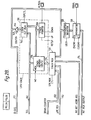
microprogram sequence controller 10 having the specific internal architecture shown in Fig. 2, it is understood that the internal structure, the type of internal elements, the number of bits processed thereby, and so forth, may vary from implementation to implementation while still providing the various benefits of the invention. - The
controller 10 shown in Fig. 2 is identical in all respects except as will be described hereinafter to the controller shown in Fig. 2 of the related copending application U.S. Serial No. 608,319, filed May 8, 1984, on behalf of Ole Moller and Sanjay Iyer entitled "Interruptible Structured Microprogrammed 16-Bit Address Sequence Controller" and assigned to the assignee of the instant application, and is hereby incorporated by reference in the instant application. Except insofar as will be described hereinafter regarding the interrupt/trap handling aspects of the controller of the instant invention, a detailed description of the controller of the instant invention is supplied in the related copending application. The microinstruction set supported by the instant controller is identical in all relevant respects to the instruction set described in the related copending application. - Fig. 2A of the instant application is identical in all respects with Fig. 2A of the related copending application, and the detailed description therein applies equally to Fig. 2A of the instant application in all respects, except for the provision of the set of input terminals, collectively denoted INTR/TRP in Fig. 1 of the instant application, including a force continue (FC) input to the
controller 10, an interrupt enable (INTEN) input, an interrupt request (INTR) input and an interrupt acknowledge (INTA) output connected to the interruptlogic circuit 176, renamed interrupt/trap logic circuit 176 in the instant Fig. 2A, the relative locations of the microprogram counter (MPC) register 154 and theincrementer 158, and the presence of signal lines communicating signals from the interrupt/trap logic circuit 176 to a disable (DIS) input ofCONTROL 100 and to a hold Z (HOLD Z) input ofincrementer 158, and for the presence of a signal line communicating a signal from a complemented carry-in (C IN) input terminal ofcontroller 10 to theincrementer 158. The C IN terminal is part of the set of input terminals denoted INTR/TRP on Fig. 1. (Fig. 2B of the instant application and Fig. 2B of the related copending application are identical in all respects, and the description therein applies equally to Fig. 2B of the instant application in all respects). - The
microprogram sequence controller 10 of the instant invention can handle an asynchronous event if the controller is enabled to receive interrupts or configured to receive a trap and is not being reset or held, i.e. a HIGH is applied to an interrupt enable (INTEN) and an interrupt request (INTR) terminal ofcontroller 10 and a LOW is applied to a RESET and a HOLD terminal. If a HIGH is applied to a force continue (FC) terminal and to a complemented carry-in to incrementer (C_IN) terminal then a trap can be received. - With reference to Fig. 2A of the instant application, an interrupt/
trap logic circuit 176 receives at an input I1, the signal received at the interrupt request (INTR) terminal ofcontroller 10. Interrupt/trap logic circuit 176 ALU has communicated to a set of inputs I2, I3, I4, I5 and I6 signals received at the five other input terminals ofcontroller 10 mentioned above; the signal at the interrupt enable (INTEN) input terminal to input I2, the signal at the reset (RESET) input terminal to input I3, the signal at the HOLD input terminal to input I4, the signal at the slave (SLAVE) input terminal to input I5 and the signal at the force continue (FC) terminal to input I6. An interrupt acknowledge (INTA) output terminal ofcontroller 10 is connected to an output (O) of the interrupt/trap logic circuit 176. - A signal representing the occurrence of a HIGH, at the FC or HOLD terminals of
controller 10 is also conducted to a disable (DIS) input of combinational logic circuit (CONTROL) 150 which if HIGH, coversCONTROL 100 to generate signals which override the instruction word received at the INST inputs IO-5 ofCONTROL 100, as will be described below, in connection with Fig. 3. - In addition to the signal conducted to the disable (DIS) input,
CONTROL 100 receives from the interrupt/trap logic circuit 176 signals conducted to a force continue or hold (FCH Z) input and an interrupt processing (INT Z) input. TheCONTROL 100 also receives the signal at the FC terminal ofcontroller 10. A complete description of those signals will be given in connection with the explanation of Figs. 3A, 3B and 3C, below. - The function and meaning of the signals at the RESET, SLAVE, HOLD and INTA terminals of
controller 10 are as described in the related copending application. - Unlike their descriptions in the related copending application of the
microprogram sequence controller 10, the microprogram counter (MPC) register 154 of the instant invention contains the address of the currently-executed microinstruction, and theincrementer 158 contains the address of the currently-executed microinstruction plus one and is used to point to the next microinstruction to be executed if no branching is to be performed. The MPC register 154 receives the address at the output of interrupt multiplexer (INT MUX) 172 via signal lines 174. MPC register 154 also receives the clock pulse CLK at each clock cycle. The resulting contents is conducted alongsignal lines 156 from the MPC register 154 to theincrementer 158, providing the "current address plus one" to theADDR MUX 116 and theSTACK MUX 132 via signal lines 152.Incrementer 158 also receives the signal applied to the complemented carry-in (C IN) terminal ofcontroller 10. If the carry-in to the incrementer C IN is a HIGH, theincrementer 158 is inhibited and the address received from MPC register 154 onsignal lines 156 is conducted unchanged onto thesignal lines 152, if the C_IN is a LOW, theincrementer 158 adds one to the address received from the MPC register before it is placed onto the signal lines 152. - Referring again to Fig. 2A of the instant application, the sixteen
signal lines 162 forming the output ofADDR MUX 116 are communicated to a set (of sixteen) three-state output drivers 164. Thedrivers 164 place the 16-bit branch address determined bymicroprogram sequence controller 10 onto a three-state, bidirectional Y-bus 166 provided to receive, conduct and transmit the data signals to the DATA_OUT terminals ofcontroller 10. The three-state output drivers 164 are enabled by a HIGH received on asignal line 168.Signal line 168 is the output of an NORgate 170 which is controlled by signals received at a SLAVE input, a HOLD input terminal ofmicroprogram sequence controller 10, and a signal (INT) generated by an interruptlogic circuit 176. When these three signals are LOW, NORgate 170 setsline 168 HIGH and the outputs of three-state drivers 164 are enabled. The address signals onlines 162 may then be applied to Y-bus 166 and presented to the DATA OUT terminals ofcontroller 10. - When the signal on
line 168 to three-state output drivers 164 is a LOW, the outputs of the three-state output drivers are in the high impedance state and an address signal may then be applied to the "Y" address bus 32 (Fig. 1) by the IVP 58 (Fig. 1) to select the next microinstruction, as will be described below. -
Address signal lines 162 are also coupled to an interrupt multiplexer (INT MUX) 172 which can conduct branch addresses present on Y-bus 166 to MPC register 154 andcomparator 129 via signal lines 174. Furthermore, the DATA OUT terminals can receive an interrupt address and conduct it along Y-bus 166 to an interrupt multiplexer (INT MUX) 172, as will be described below. An interrupt return address register (INT RET ADDR REG) 175 is used to temporarily hold the return address of the interrupted or trapped microprogram when an interrupt or trap request is received by themicroprogram sequence controller 10. - In all other respects, the structure and operation of the
microprogram sequence controller 10 as shown in Fig. 2A of the instant application is essentially identical to the structure and operation of themicroprogram sequence controller 10 as shown in Fig. 2A of the related copending application, as it relates to the handling of interrupts. To reiterate briefly, when there is no interrupt or trap request supplied to sequencecontroller 10 and it is not being operated in the slave mode and not being held, branch addresses are conducted from ADDRMUX output lines 162 to the DATA OUT terminals via Y-bus 166 and three-state output drivers 164. Furthermore, under these conditions, interrupt/trap logic circuit 176 codes the received inputs and generates interrupt signal (INT) communicated toINT MUX 172 online 178 so that the branch addresses input toINT MUX 172 are passed alongsignal lines 174 to the MPC register 154 andcomparator 129. - When an interrupt is to be processed by
microprogram sequence controller 10, the current microinstruction can safely be permitted to finish execution. At the start of the next controller clock cycle, however, INTEN is HIGH, RESET and HOLD are LOW and interrupt/trap logic circuit 176 causes an interrupt (INT) signal to change from LOW to HIGH and this HIGH signal is communicated vialine 178 toINT MUX 172 which disables the address communication path from theADDR MUX 116 to MPC register 154 andcomparator 129 via Y-bus 166 andsignal lines 174. Furthermore, Y-bus three-state output drivers 164 are disabled by virtue of NORgate 170 sending a LOW signal alongline 168 todrivers 164, in response to the HIGH INT signal generated by interrupt/trap logic circuit 176. The Y-bus 166, in addition to conducting the outputs of the three-state output drivers 164 to the DATA OUT terminals, is also connected to an input to theINT MUX 172 which, as mentioned earlier, has its output connected viasignal line 174 to the MPC register 154 and therefrom viasignal lines 156 to theincrementer 158 which increments the address supplied by theIVP 58. - Accordingly, presence of the HIGH INT signal on
line 178 causesINT MUX 172 to select the input receiving the signals on the bidirectional Y-bus 166 from the DATA OUT terminals ofcontroller 10, namely the interrupt address. This interrupt address is then conducted via theoutput signal lines 174 of theINT MUX 172 to the MPC register 154 and thecomparator 129. The address from theADDR MUX 116 is saved by storing it in the interruptreturn address register 175 and during the next clock cycle pushed onto theLIFO stack 130. The interrupt routine causes the content of certain of the registers to be stored in theLIFO STACK 130, which can be retrieved later. The information stored provides an address linkage return to the microinstruction sequence that themicroprogram sequence controller 10 was in when it received an interrupt request. Since this return address is saved on theLIFO STACK 130, nested interrupts can be handled by amicroprogram sequence controller 10 constructed according to the teaching of the instant invention. - In order to ensure that all information needed to establish the linkage back to the sequence interrupted, yet proceed with the branching and executing of the interrupt subroutine to which the branch occurs, all information is stored in one clock period. Accordingly, certain of the information is temporarily stored in the INT
RET ADDR REG 175 which is then communicated to theLIFO stack 130 via theSTACK MUX 132. The INTRET ADD REG 175 receives the clock (CLK), provided at and communicated from the CP input terminal, at its clock (CL) input. Information is stored in the interrupt return address register 175 every clock (instruction) cycle; but the stored information is used only when an interrupt signal is received. - When the
microprogram sequence controller 10 is enabled to detect traps, at the occurrence of a trapped event the current microinstruction must be aborted before the end of the current controller clock cycle and re-executed after the execution of a trap routine, which is designed to take intervening corrective measures. As soon as thecontroller 10 receives those inputs signalling the occurrence of an event to be trapped, i.e., INTEN, INTR, FC and C IN are HIGH, interrupt/trap logic circuit 176 immediately causes the interrupt (INT) signal to change from LOW to HIGH and this HIGH signal is communicated vialine 178 toINT MUX 172 which, as in the case of an interrupt, disables the address communication path from theADDR MUX 116 to the MPC register 154 andcomparator 129 via Y-bus 166 andsignal lines 174. Furthermore, Y-bus three-state output drivers 164 are disabled by virtue of NORgate 170 sending a LOW signal alongline 168 todrivers 164, in response to the HIGH INT signal generated by inter- rupt/logic circuit 176. - Accordingly, presence of the HIGH INT signal on
line 178 causesINT MUX 172 to select the input receiving the signals on the bidirectional Y-bus 166 from the DATA_OUT terminals ofcontroller 10, namely the address of the trap routine. This trap address is then conducted via theoutput signal lines 174 of theINT MUX 172 to the MPC register 154 (and the comparator 129). - Due to the relative positions of the
incrementer 158 and the MPC register 154 within thecontroller 10, the address present at the output of theincrementer 158, which is the trap return address, i.e., the address of the aborted microinstruction, is available to be conducted viasignal lines 152 to theADDR MUX 116 and saved by storing it in the INT RET ADDR REG 175 (and during the next clock cycle) pushed onto theLIFO STACK 130, at the same time that the trap address is being stored in the MPC register 154, as described above. - Since the C-IN signal received at the
incrementer 158 is a HIGH, the trap address received by the incrementer viasignal lines 156 will be conducted unchanged via thesignal lines 152 to theADDR MUX 116. Due to the fact that the FC signal input to themicroprogram sequence controller 10 is a HIGH, a HIGH signal is generated by interrupt/trap logic circuit 176 and conducted to the DIS input of theCONTROL 100.CONTROL 100 then generates a signal communicated to the COND input ofADDR MUX 116, which causesADDR MUX 116 to conduct the trap return address to itsoutput lines 162. Whereupon the address of the currently-executed microinstruction is replaced on the Y-bus 166 by the address of the first microinstruction of the trap routine. Since this currently-executed microinstruction did not complete execution, due to the HIGH FC signal, the contents of the registers within themicroprogram sequencer 10 were not updated and thus upon return from the trap routine, the instruction can be re-executed without further action. The handling of the trap by themicroprogram sequence controller 10 therefore can proceed beyond this point as described above for an interrupt. - The signals received by
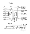
microprogram sequence controller 10 at its interrupt request (INTR) and interrupt enable (INTEN) terminals are conducted to the interrupt/trap logic circuit 176 at its I1, I2 inputs, respectively. These signals are latched by the interrupt/trap detectcircuit 200 illustrated in Fig. 3A. As shown, a pair of flip-flops flop 202 receives at its data (D) input the interrupt signal (INT) generated by a NORgate 206 which, in turn, receives the INTR, INTEN, terminals viainverters 208 and 210 and the signals conducted from the controller HOLD and RESET terminals, each at a complemented input ofgate 206. Accordingly, the true (Q) output of flip-flop 202 is the logical AND of the signal at the INTR terminal and the signal at the INTEN terminal from the preceding clock cycle, if themicroprogram sequence controller 10 is not being held or reset. This Q output signal (INT Z) is received at the complemented input to an AND gate 216. - In similar fashion, the data (D) input of the flip-
flop 204 receives the signal on the signal line conducting the signal from the HOLD terminal ofcontroller 10. The signal at a first true (Q) output of flip-flop 204 is received at an input to a wired-OR gate 218. The signal at a second true (Q) output of flip-flop 204 forms the HOLD Z signal output from interrupt/ trap detectcircuit 200.Gate 218 also receives at a second input the signal conducted from thecontroller 10 force continue (FC) terminal. Since the signal at the HOLD terminal is latched by flip-flop 204, the output of the wired-OR gate 218, force continue hold (FCH_Z) will follow the present state of the FC terminal during any clock cycle when themicroprogram sequence controller 10 is not being held. Accordingly, the output signal FCH_Z is applied to the disable (DIS) input ofCONTROL 100 which causes the currently-applied microinstruction bits IO-5 to be ignored and causes all output signals generated byCONTROL 100 to be inactive, other than causing a CMUXCTL to be generated which deselects any of the inputs to theCMUX 118 onlines ADDR MUX 116 to select the inputs onlines 152 from theincrementer 158 to be placed on the output of theADDR MUX 116 and conducted viasignal lines 162 to the INTRET ADDR REG 175. - The signal INT generated at the output of NOR
gate 206 is conducted viasignal line 178 to an input of the NORgate 170, which in turn generates a signal online 168 causing the set of sixteen three-state output drivers 164 to achieve the high impedance state. This disconnects Y-bus 166 from ADDRMUX output lines 162. The INT signal is also conducted to theINT MUX 172 where it causes the interrupt/trap address placed on the Y-bus 166 by theIVP 58 to be conducted to the MPC REGISTER 154 via signal lines 174. - Interrupt/
trap detection circuit 200 includes a NOR gate 222 which receives at inputs the signal on the SLAVE and HOLD terminals ofcontroller 10 via inverters 224 and 212; respectively. The output of NOR gate 222 is connected to inverting the enable input of a three-state buffer 226. The output of NORgate 206, the INT signal, is passed through the invertingbuffer 226 to become the INTA signal that enables (via its OE input) the IVP 58 (Fig. 1). - Accordingly, if the currently-executing microinstruction is "trapped," the address of the currently-executing microinstruction is saved in the INT
RET ADDR REG 175, as follows: during a trap theincrementer 158 receives a HIGH signal from the C_IN terminal of controller to which, as shown in Fig. 3B, is conducted via aninverter 250 to an input of a wired-OR gate 252. The HOLD_Z signal generated by the flip-flop 204 is conducted to a second input of the wired-OR gate 252. The HOLD-Z signal is a LOW since thecontroller 10 is, by assumption, not being held, both inputs to wired-OR gate 252 are LOW and the resulting LOW output is received byincrement circuit 254 which causesincrementer 158 to pass the address of the currently-executing microinstruction received onsignal lines 156 unincremented, i.e. the trap return address, ontosignal lines 152 where it is selected byADDR MUX 116 to be passed to the INTRET ADDR REG 175. - At the same time,
INT MUX 172 receives the address of the first instruction of the trap routine and passes it to the input of the MPC register 154 vialines 174. At the next clock cycle, this address is received by theincrementer 158 onsignal lines 156 and since a LOW carry-in C_IN signal is now received by theincrementer 158, the address of the instruction next-following the first instruction of the trap routine is presented.to theADDR MUX 116 viabus 152. Since the trap return address is present at the output of the INTRET ADDR REG 172 it is pushed onto theLIFO STACK 130 by the first instruction of the trap routine, and accordingly this first instruction may not use theLIFO STACK 130. The final instruction of the trap routine will pop this trap address from theLIFO STACK 130 and since it was not incremented prior to its push onto the stack, as mentioned, themicroprogram sequence controller 10 will issue the trap return address on theDATA_OUT terminal 166 upon return from the trap routine and accordingly the trapped microinstruction will be re-issued following execution of the trap routine. As mentioned above, since trap return addresses are pushed onto theLIFO STACK 130, traps may be nested. - As mentioned above, since the FC terminal of the
controller 10 is tied HIGH during a trap, the outputs of theCONTROL 100, other than the CMUXCTL signal and the COND signal previously described, are inactive and the currently-executing microinstruction bits 10-5 are ignored for the duration of the present controller clock cycle. Thus, other than the actions just described regarding the storage of the trap return address in the INTRET ADDR REG 175 and the storage of the address of the trap routine in the MPC register 154, the trapped instruction is aborted. - Alternatively, if the currently-executing microinstruction is "interrupted," i.e. the FC terminal of
controller 10 is LOW, the presently-executing microinstruction will complete execution since the FCH Z signal output from the wired-OR gate 218 is LOW throughout the remainder of the controller's present clock cycle. Hence theCONTROL 100 will proceed to generate all the signals it normally would. However, during the present clock cycle, the NORgate 206, at the time the interrupt is activated, will pass the signal from the INTR terminal ofcontroller 10 and the resulting signal INT will be conducted onsignal line 178 to the NORgate 170 which will cause the three-state output drivers 164 to disconnect the Y-bus 166 from theADDR MUX 116output lines 162 and the INT MUX 172 causes the interrupt address to be conducted to the MPC register 154 as mentioned above. - Accordingly, the address of the currently-executing microinstruction is saved in the INT
RET ADDR REG 175 since during an interrupt the C_IN terminal is HIGH and thus theincrementer 158 passes the address of the currently-executing microinstruction received onsignal lines 156 onto signal lines 154 where it is selected by theADDR MUX 116 to be passed to the INTRET ADDR REG 175. At the same time,INT MUX 172 receives the address of the first instruction of the interrupt routine and passes it to the input of the MPC register 154 vialines 174. At the next clock cycle, this address is received by theincrementer 158 and incremented as explained above in connection with the trap-handling bycontroller 10. Similarly, the final instruction of the interrupt routine will pop this interrupt return address from theLIFO STACK 130, themicroprogram sequence controller 10 will issue the interrupt return address on theDATA OUT terminals 166 upon return from the interrupt routine and accordingly the microinstruction next following the interrupted microinstruction will be executed following completion of the interrupt routine. As mentioned above, since interrupt return addresses are pushed onto theLIFO stack 130, interrupts may be nested.
Claims (6)
Priority Applications (1)
| Application Number | Priority Date | Filing Date | Title |
|---|---|---|---|
| AT85307899T ATE77159T1 (en) | 1984-11-01 | 1985-10-31 | MICROPROGRAM SEQUENCE CONTROL UNIT. |
Applications Claiming Priority (2)
| Application Number | Priority Date | Filing Date | Title |
|---|---|---|---|
| US06/667,242 US4719565A (en) | 1984-11-01 | 1984-11-01 | Interrupt and trap handling in microprogram sequencer |
| US667242 | 1984-11-01 |
Publications (3)
| Publication Number | Publication Date |
|---|---|
| EP0180476A2 true EP0180476A2 (en) | 1986-05-07 |
| EP0180476A3 EP0180476A3 (en) | 1988-11-09 |
| EP0180476B1 EP0180476B1 (en) | 1992-06-10 |
Family
ID=24677423
Family Applications (1)
| Application Number | Title | Priority Date | Filing Date |
|---|---|---|---|
| EP85307899A Expired - Lifetime EP0180476B1 (en) | 1984-11-01 | 1985-10-31 | Microprogramme sequence controller |
Country Status (5)
| Country | Link |
|---|---|
| US (1) | US4719565A (en) |
| EP (1) | EP0180476B1 (en) |
| JP (1) | JPS61110239A (en) |
| AT (1) | ATE77159T1 (en) |
| DE (1) | DE3586195T2 (en) |
Cited By (4)
| Publication number | Priority date | Publication date | Assignee | Title |
|---|---|---|---|---|
| GB2191616A (en) * | 1986-06-10 | 1987-12-16 | Etat Represente Par Le Secreta | Microprogrammed processor |
| GB2196454A (en) * | 1986-10-24 | 1988-04-27 | Brother Ind Ltd | Data processing system |
| FR2681963A1 (en) * | 1991-08-30 | 1993-04-02 | Intel Corp | TRANSPARENT INTERRUPTIONS FOR THE SYSTEM WITH AUTOMATIC RESTART OF INPUT / OUTPUT SEQUENCE. |
| US5479652A (en) * | 1992-04-27 | 1995-12-26 | Intel Corporation | Microprocessor with an external command mode for diagnosis and debugging |
Families Citing this family (24)
| Publication number | Priority date | Publication date | Assignee | Title |
|---|---|---|---|---|
| JPS6282402A (en) * | 1985-10-07 | 1987-04-15 | Toshiba Corp | Sequence controller |
| JPS6362039A (en) * | 1986-09-03 | 1988-03-18 | Mitsubishi Electric Corp | Computer |
| EP0270081B1 (en) * | 1986-12-01 | 1995-05-10 | Nec Corporation | Microprogram controller receiving interrupt request during instruction execution |
| US4980821A (en) * | 1987-03-24 | 1990-12-25 | Harris Corporation | Stock-memory-based writable instruction set computer having a single data bus |
| US5053952A (en) * | 1987-06-05 | 1991-10-01 | Wisc Technologies, Inc. | Stack-memory-based writable instruction set computer having a single data bus |
| US4890221A (en) * | 1988-04-01 | 1989-12-26 | Digital Equipment Corporation | Apparatus and method for reconstructing a microstack |
| US5134693A (en) * | 1989-01-18 | 1992-07-28 | Intel Corporation | System for handling occurrence of exceptions during execution of microinstructions while running floating point and non-floating point instructions in parallel |
| US4951194A (en) * | 1989-01-23 | 1990-08-21 | Tektronix, Inc. | Method for reducing memory allocations and data copying operations during program calling sequences |
| US5327567A (en) * | 1989-11-16 | 1994-07-05 | Texas Instruments Incorporated | Method and system for returning emulated results from a trap handler |
| US5463778A (en) * | 1989-11-16 | 1995-10-31 | Texas Instruments Incorporated | User controlled trap handler |
| US5103476A (en) * | 1990-11-07 | 1992-04-07 | Waite David P | Secure system for activating personal computer software at remote locations |
| DE4211245B4 (en) * | 1991-04-05 | 2009-05-14 | Kabushiki Kaisha Toshiba, Kawasaki | Processor system in parallel processing type and method for its control |
| EP0522513A2 (en) * | 1991-07-09 | 1993-01-13 | Hughes Aircraft Company | High speed parallel microcode program controller |
| US5517624A (en) * | 1992-10-02 | 1996-05-14 | Compaq Computer Corporation | Multiplexed communication protocol between central and distributed peripherals in multiprocessor computer systems |
| US5680645A (en) * | 1992-11-18 | 1997-10-21 | Canon Kabushiki Kaisha | System for executing first and second independently executable programs until each program relinquishes control or encounters real time interrupts |
| JPH06274354A (en) * | 1993-03-12 | 1994-09-30 | Internatl Business Mach Corp <Ibm> | Method and system for control of operation of destructive hardware |
| US5745770A (en) * | 1993-12-27 | 1998-04-28 | Intel Corporation | Method and apparatus for servicing simultaneous I/O trap and debug traps in a microprocessor |
| DE19535546B4 (en) * | 1995-09-25 | 2004-04-08 | Siemens Ag | Method for operating a real-time computer system controlled by a real-time operating system |
| US5778221A (en) * | 1997-03-17 | 1998-07-07 | International Business Machines Corporation | System for executing asynchronous branch and link in parallel processor |
| JP4018158B2 (en) * | 1997-10-02 | 2007-12-05 | コーニンクレッカ フィリップス エレクトロニクス エヌ ヴィ | Variable instruction set computer |
| US6816934B2 (en) * | 2000-12-22 | 2004-11-09 | Hewlett-Packard Development Company, L.P. | Computer system with registered peripheral component interconnect device for processing extended commands and attributes according to a registered peripheral component interconnect protocol |
| US20050182920A1 (en) * | 2004-02-13 | 2005-08-18 | Alexandre Palus | Apparatus and method for expedited exception handling using a dedicated port |
| US7930589B2 (en) * | 2005-06-17 | 2011-04-19 | Analog Devices, Inc. | Interrupt-responsive non-volatile memory system and method |
| WO2007048988A1 (en) * | 2005-10-26 | 2007-05-03 | Arm Limited | A data processing apparatus and method for handling procedure call instructions |
Citations (3)
| Publication number | Priority date | Publication date | Assignee | Title |
|---|---|---|---|---|
| US3909802A (en) * | 1974-04-08 | 1975-09-30 | Honeywell Inf Systems | Diagnostic maintenance and test apparatus |
| US4141068A (en) * | 1977-03-24 | 1979-02-20 | Xerox Corporation | Auxiliary ROM memory system |
| US4398244A (en) * | 1980-05-07 | 1983-08-09 | Fairchild Camera & Instrument Corporation | Interruptible microprogram sequencing unit and microprogrammed apparatus utilizing same |
Family Cites Families (8)
| Publication number | Priority date | Publication date | Assignee | Title |
|---|---|---|---|---|
| US4074353A (en) * | 1976-05-24 | 1978-02-14 | Honeywell Information Systems Inc. | Trap mechanism for a data processing system |
| JPS5341496A (en) * | 1977-05-11 | 1978-04-14 | Yoshio Watanabe | Tobacco leaves arranging apparatus equipped with safety device |
| US4339796A (en) * | 1978-06-30 | 1982-07-13 | International Business Machines Corporation | System for generating a plurality of different addresses for a working memory of a microcontroller during execution of certain instructions |
| US4241399A (en) * | 1978-10-25 | 1980-12-23 | Digital Equipment Corporation | Calling instructions for a data processing system |
| FR2474200B1 (en) * | 1980-01-22 | 1986-05-16 | Bull Sa | METHOD AND DEVICE FOR ARBITRATION OF ACCESS CONFLICTS BETWEEN AN ASYNCHRONOUS QUERY AND A PROGRAM IN CRITICAL SECTION |
| US4438492A (en) * | 1980-08-01 | 1984-03-20 | Advanced Micro Devices, Inc. | Interruptable microprogram controller for microcomputer systems |
| JPS5958549A (en) * | 1982-09-29 | 1984-04-04 | Hitachi Ltd | Microprogram control system |
| US4589065A (en) * | 1983-06-30 | 1986-05-13 | International Business Machines Corporation | Mechanism for implementing one machine cycle executable trap instructions in a primitive instruction set computing system |
-
1984
- 1984-11-01 US US06/667,242 patent/US4719565A/en not_active Expired - Lifetime
-
1985
- 1985-10-31 DE DE8585307899T patent/DE3586195T2/en not_active Expired - Lifetime
- 1985-10-31 AT AT85307899T patent/ATE77159T1/en not_active IP Right Cessation
- 1985-10-31 JP JP60246099A patent/JPS61110239A/en active Granted
- 1985-10-31 EP EP85307899A patent/EP0180476B1/en not_active Expired - Lifetime
Patent Citations (3)
| Publication number | Priority date | Publication date | Assignee | Title |
|---|---|---|---|---|
| US3909802A (en) * | 1974-04-08 | 1975-09-30 | Honeywell Inf Systems | Diagnostic maintenance and test apparatus |
| US4141068A (en) * | 1977-03-24 | 1979-02-20 | Xerox Corporation | Auxiliary ROM memory system |
| US4398244A (en) * | 1980-05-07 | 1983-08-09 | Fairchild Camera & Instrument Corporation | Interruptible microprogram sequencing unit and microprogrammed apparatus utilizing same |
Non-Patent Citations (1)
| Title |
|---|
| ELECTRONICS, vol. 53, no. 22, October 1980, pages 139-143, New York US; "Technical articles: The system/370 processor chip: a triumph for automated design" * |
Cited By (6)
| Publication number | Priority date | Publication date | Assignee | Title |
|---|---|---|---|---|
| GB2191616A (en) * | 1986-06-10 | 1987-12-16 | Etat Represente Par Le Secreta | Microprogrammed processor |
| GB2191616B (en) * | 1986-06-10 | 1990-12-12 | France Etat Poste Telecomm | A microprogrammed processor for the resolution of logic programs |
| GB2196454A (en) * | 1986-10-24 | 1988-04-27 | Brother Ind Ltd | Data processing system |
| GB2196454B (en) * | 1986-10-24 | 1991-01-09 | Brother Ind Ltd | Data processing system |
| FR2681963A1 (en) * | 1991-08-30 | 1993-04-02 | Intel Corp | TRANSPARENT INTERRUPTIONS FOR THE SYSTEM WITH AUTOMATIC RESTART OF INPUT / OUTPUT SEQUENCE. |
| US5479652A (en) * | 1992-04-27 | 1995-12-26 | Intel Corporation | Microprocessor with an external command mode for diagnosis and debugging |
Also Published As
| Publication number | Publication date |
|---|---|
| EP0180476A3 (en) | 1988-11-09 |
| DE3586195D1 (en) | 1992-07-16 |
| ATE77159T1 (en) | 1992-06-15 |
| DE3586195T2 (en) | 1992-12-03 |
| EP0180476B1 (en) | 1992-06-10 |
| JPS61110239A (en) | 1986-05-28 |
| US4719565A (en) | 1988-01-12 |
| JPH0529933B2 (en) | 1993-05-06 |
Similar Documents
| Publication | Publication Date | Title |
|---|---|---|
| EP0180476B1 (en) | Microprogramme sequence controller | |
| US4438492A (en) | Interruptable microprogram controller for microcomputer systems | |
| US4868735A (en) | Interruptible structured microprogrammed sixteen-bit address sequence controller | |
| US4181934A (en) | Microprocessor architecture with integrated interrupts and cycle steals prioritized channel | |
| US4047161A (en) | Task management apparatus | |
| US4016545A (en) | Plural memory controller apparatus | |
| EP0464494B1 (en) | A high performance pipelined emulator | |
| US4415969A (en) | Macroinstruction translator unit for use in a microprocessor | |
| US4447873A (en) | Input-output buffers for a digital signal processing system | |
| US4166289A (en) | Storage controller for a digital signal processing system | |
| US4378589A (en) | Undirectional looped bus microcomputer architecture | |
| US4200912A (en) | Processor interrupt system | |
| EP0024288A2 (en) | Computer system having at least two processors with shared storage | |
| US4268908A (en) | Modular macroprocessing system comprising a microprocessor and an extendable number of programmed logic arrays | |
| US4339793A (en) | Function integrated, shared ALU processor apparatus and method | |
| CA1080364A (en) | Microprogrammed control of foreign processor control functions | |
| US5193159A (en) | Microprocessor system | |
| US4349872A (en) | Interrupt control system | |
| US4764865A (en) | Circuit for allocating memory cycles to two processors that share memory | |
| US4225921A (en) | Transfer control technique between two units included in a data processing system | |
| US4320454A (en) | Apparatus and method for operand fetch control | |
| EP0010196A1 (en) | Control circuit and process for digital storage devices | |
| US5068821A (en) | Bit processor with powers flow register switches control a function block processor for execution of the current command | |
| US4371931A (en) | Linear micro-sequencer for micro-processor system utilizing specialized instruction format | |
| US4217639A (en) | Logic for generating multiple clock pulses within a single clock cycle |
Legal Events
| Date | Code | Title | Description |
|---|---|---|---|
| PUAI | Public reference made under article 153(3) epc to a published international application that has entered the european phase |
Free format text: ORIGINAL CODE: 0009012 |
|
| AK | Designated contracting states |
Kind code of ref document: A2 Designated state(s): AT BE CH DE FR GB IT LI LU NL SE |
|
| PUAL | Search report despatched |
Free format text: ORIGINAL CODE: 0009013 |
|
| AK | Designated contracting states |
Kind code of ref document: A3 Designated state(s): AT BE CH DE FR GB IT LI LU NL SE |
|
| 17P | Request for examination filed |
Effective date: 19890214 |
|
| 17Q | First examination report despatched |
Effective date: 19910313 |
|
| GRAA | (expected) grant |
Free format text: ORIGINAL CODE: 0009210 |
|
| AK | Designated contracting states |
Kind code of ref document: B1 Designated state(s): AT BE CH DE FR GB IT LI LU NL SE |
|
| PG25 | Lapsed in a contracting state [announced via postgrant information from national office to epo] |
Ref country code: SE Effective date: 19920610 Ref country code: LI Effective date: 19920610 Ref country code: IT Free format text: LAPSE BECAUSE OF FAILURE TO SUBMIT A TRANSLATION OF THE DESCRIPTION OR TO PAY THE FEE WITHIN THE PRESCRIBED TIME-LIMIT;WARNING: LAPSES OF ITALIAN PATENTS WITH EFFECTIVE DATE BEFORE 2007 MAY HAVE OCCURRED AT ANY TIME BEFORE 2007. THE CORRECT EFFECTIVE DATE MAY BE DIFFERENT FROM THE ONE RECORDED. Effective date: 19920610 Ref country code: CH Effective date: 19920610 Ref country code: BE Effective date: 19920610 Ref country code: AT Effective date: 19920610 |
|
| REF | Corresponds to: |
Ref document number: 77159 Country of ref document: AT Date of ref document: 19920615 Kind code of ref document: T |
|
| REF | Corresponds to: |
Ref document number: 3586195 Country of ref document: DE Date of ref document: 19920716 |
|
| REG | Reference to a national code |
Ref country code: CH Ref legal event code: PL |
|
| ET | Fr: translation filed | ||
| PG25 | Lapsed in a contracting state [announced via postgrant information from national office to epo] |
Ref country code: LU Free format text: LAPSE BECAUSE OF NON-PAYMENT OF DUE FEES Effective date: 19921031 |
|
| PLBE | No opposition filed within time limit |
Free format text: ORIGINAL CODE: 0009261 |
|
| STAA | Information on the status of an ep patent application or granted ep patent |
Free format text: STATUS: NO OPPOSITION FILED WITHIN TIME LIMIT |
|
| 26N | No opposition filed | ||
| REG | Reference to a national code |
Ref country code: GB Ref legal event code: IF02 |
|
| PGFP | Annual fee paid to national office [announced via postgrant information from national office to epo] |
Ref country code: GB Payment date: 20020913 Year of fee payment: 18 |
|
| PGFP | Annual fee paid to national office [announced via postgrant information from national office to epo] |
Ref country code: NL Payment date: 20020919 Year of fee payment: 18 |
|
| PGFP | Annual fee paid to national office [announced via postgrant information from national office to epo] |
Ref country code: FR Payment date: 20021003 Year of fee payment: 18 |
|
| PGFP | Annual fee paid to national office [announced via postgrant information from national office to epo] |
Ref country code: DE Payment date: 20021031 Year of fee payment: 18 |
|
| PG25 | Lapsed in a contracting state [announced via postgrant information from national office to epo] |
Ref country code: GB Free format text: LAPSE BECAUSE OF NON-PAYMENT OF DUE FEES Effective date: 20031031 |
|
| PG25 | Lapsed in a contracting state [announced via postgrant information from national office to epo] |
Ref country code: NL Free format text: LAPSE BECAUSE OF NON-PAYMENT OF DUE FEES Effective date: 20040501 Ref country code: DE Free format text: LAPSE BECAUSE OF NON-PAYMENT OF DUE FEES Effective date: 20040501 |
|
| GBPC | Gb: european patent ceased through non-payment of renewal fee |
Effective date: 20031031 |
|
| PG25 | Lapsed in a contracting state [announced via postgrant information from national office to epo] |
Ref country code: FR Free format text: LAPSE BECAUSE OF NON-PAYMENT OF DUE FEES Effective date: 20040630 |
|
| NLV4 | Nl: lapsed or anulled due to non-payment of the annual fee |
Effective date: 20040501 |
|
| REG | Reference to a national code |
Ref country code: FR Ref legal event code: ST |