EP0169387A2 - Microscope - Google Patents
Microscope Download PDFInfo
- Publication number
- EP0169387A2 EP0169387A2 EP85107775A EP85107775A EP0169387A2 EP 0169387 A2 EP0169387 A2 EP 0169387A2 EP 85107775 A EP85107775 A EP 85107775A EP 85107775 A EP85107775 A EP 85107775A EP 0169387 A2 EP0169387 A2 EP 0169387A2
- Authority
- EP
- European Patent Office
- Prior art keywords
- optical system
- objective
- stage
- sample
- objective optical
- Prior art date
- Legal status (The legal status is an assumption and is not a legal conclusion. Google has not performed a legal analysis and makes no representation as to the accuracy of the status listed.)
- Granted
Links
Images


Classifications
-
- G—PHYSICS
- G02—OPTICS
- G02B—OPTICAL ELEMENTS, SYSTEMS OR APPARATUS
- G02B21/00—Microscopes
- G02B21/24—Base structure
Definitions
- This invention relates to a microscope whereby a sample can be observed over a wide range.
- a microscope is formed fundamentally of an objective, an eyepiece and a stage for holding a sample observing position, the sample held on the stage or the stage itself used to be moved in the direction vertical to the optical axis.
- the stage mounting the sample must be moved in a wide range, that is, over the range B which is 4 times as large as the range A to be observed in Fig. 1, therefore the strength of the entire microscope including the stage is required and the stage moving mechanism must be large.
- the stage moving range will become 4 times as large, therefore, the entire microscope will be larger, the inertia of the,stage itself will be larger and therefore the position precision will be more difficult to control.
- a primary object of the present invention is to provide a microscope whereby the sample observing position can be varied over a wide range without requiring a large objective.
- this object can be attained by moving the objective optical system parallelly with the visual field plane to make the light path length of a part of the observing optical system free to extend and contract.
- Another, object of the present invention is to simplify the entire structure of this kind of microscope and to lower the height of the microscope part above the sample.
- a further object of the present invention is to provide this kind of microscope wherein such other optical systems as an illuminating optical system and reference optical system can be easily and compactly incorporated into the objective optical system.
- Another further object of the present invention is to provide this kind of microscope wherein, in spite of the movement of the objective optical system in a wide range, the position of the eye point for the eyepiece will not move.
- Another further object of the present invention is to provide a microscope device which can be favorably utilized to inspect wafers and the like.
- the reference numeral 1 represents a microscope body
- 2 represents a stage movably mounted in a well known way on the microscope body
- 3 represents a sample to be observed as placed on the stage
- 4 represents an infinity objective
- 5 represents a mirror
- 6 represents a half mirror
- 7 represents an image forming lens
- 8 represents an eyepiece
- 9 represents an illuminating light source
- 10 represents a collector lens.
- the objective 4 and mirror 5 are arranged movably along the optical"axis between the mirror 5 and half mirror 6 by such mechanism as is described later.
- the light emitted out of the illuminating light source 9 will pass the half mirror 6 through the collector lens 10, will be reflected by the mirror 5 and will illuminate the sample 3 through the objective 4.
- the light coming out of the thus illuminated sample 3 will be made an afocal light by the objective 5, will be reflected by the mirror 5 and half mirror 6 and will be made to form an image in the position P by the image forming lens 7. This image will be observed through the eyepiece 8.
- the moving range C of the objective 4 may be the same as the observing range A as shown in Fig. 3.
- Fig. 4 shows the second actual embodiment of the present invention in which an objective optical system is arranged so as to move in two dimensional way.
- the reference numeral 11 represents a first mirror arranged slidably in the direction X along such guide 12 as, for example, a dovetail together with the objective 4
- 13 represents a second mirror arranged slidably in the direction Y along a guide 14'formed the same as the guide 12 integrally with the objective 4, first mirror 11 and guide 12.
- the light coming out of the sample 3 will be made an afocal light by the objective 4, will be reflected in the direction X by the first mirror 11, will be reflected in the direction Y by the second mirror 13, will be further reflected by the half mirror 6 and then will be made to form an image by the image forming lens 7.
- This image will be observed through the eyepiece 8. Therefore, by properly adjusting the light path length between the first mirror 11 and second mirror 13 with the guide 12 and the light path length between the second mirror 13 and half mirror 6 with the guide 14, the objective 4 can be moved in the directions X and Y without varying the image forming position and the sample 3 can be observed in any position.
- such large sample as a brain slice or large silicon wafer can be easily and precisely observed.
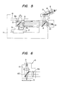
- Fig. 5 shows the third embodiment of the present invention in which an objective optical system is arranged so as to move in one dimensional way.
- the objective optical system and reflecting member are so formed as to move integrally along the optical axis
- this embodiment is fundamentally different from the embodiments shown in Figs. 2 and 4.
- the reference numeral 15 represents an objective unit including a mirror 15a and objective 15b and mounted movably along the optical axis of the objective 15b, that is, in the direction indicated by the arrow X on a guide rail 16 provided in the microscope body 1 and 17 represents a prism arranged between the image forming lens 7 and eyepiece 8 and directing obliquely upward the light having passed the image forming lens 7.
- the illuminating light progressing course to the sample 3 from the illuminating light source 9 and the observing light progressing course to the eyepiece 8 from the sample are the same as in the case of the already described embodiments.
- the observing optical system consisting of the mirror 15a, objective 15b, half mirror 6, image forming lens 7, prism 17 and eyepiece 8 as an afocal system is made between the objective 15b and image forming lens 7, by sliding the objective unit 15 along the guide rail 16, the mirror 15a and objective 15b can be moved along the optical axis of the objective 15b to vary the light path length between the objective 15b and half mirror 6, the stage 2 can be moved in the direction vertical to the paper surface with respect to the microscope body 1 to observe the sample 3 on the stage 2 in any second dimensional position and yet the image formation in the position P will not vary.
- the moving range of the objective 15b may be the same as the maximum width of the observing range. (See Fig. 3).
- Fig. 6 shows the fourth embodiment of the present invention.
- a half mirror 15'a is provided instead of the mirror 15a and the illuminating light source 9 and collector lens 10 are included within the objective unit 15, this embodiment is different from the embodiment shown in Fig. 5.
- the collector lens 10 and illuminating light source 9 are arranged above the half mirror 15'a.
- the operation is made the same as in the embodiment in Fig. 5 but, as the illuminating optical system is incorporated within the objective unit, there are advantages that the flare will reduce, the pupil position of the illuminating optical system will be kept invariable and therefore a uniform illumination will be made..
- Fig. 7 shows the fifth embodiment of the present invention.
- the half mirror 15'a is provided instead of the mirror 15a and a master specimen 18 is included within the objective unit 15, this embodiment is different from the embodiment shown in-Fig. 5.
- the master specimen 18 is arranged in a position conjugate with the sample 3 with respect to the half mirror 15'a and is so formed that the sample 3 and master specimen 18 can be observed while being compared with each other within the same visual field.
- each of the mirror 15a and half mirror 15'a may have a predetermined curvature (such as of a parabolic or spherical surface) of the reflecting surface as shown by chain lines respectively in Figs. 5 and 6 or the mirror 15a can be rotated around the axis 0 (Fig. 5) to be minutely centered with the sample 3. If a mirror or half mirror having a reflecting surface of a proper curvature is used, the objective 15b will be'able to be omitted.
- a predetermined curvature such as of a parabolic or spherical surface
- an afocal system is formed between the objective 15b and image forming lens 7 but it is needless to say that, even in the case of a focal system, the above mentioned advantages peculiar to the respective embodiments will be obtained the same. Further, in these embodiments, as evident from the above described explanation, the height of the microscope device part to be above the sample 3 can be made comparatively low and even an objective of a long operating distance can be also used.
- the part of the afocal system will be short, therefore 'the eclipse of the pupil of the afocal system will reduce, the diameter of the image forming lens will be able to be made smaller, thus the entire microscope will be able to be made small and such very effective microscope will be obtained.
- the half mirror is arranged in front of teh objective optical system, such other optical systems with respect to the half mirror as, for example, an illuminating optical system and second reference optical system will be able to be easily incorporated without making the device large.
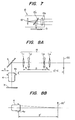
- Figs. 8A and 8H show the sixth embodiment of the present invention in which an objective optical system is arranged so as to move in one dimentional way.
- an afocal lx relay lens system consisting of a plurality of lens components is arranged between the objective optical system and eyepiece optical system so that, when the objective optical system is moved, the distances between the respective lens components forming the relay lens system, the distance between the relay lens system and objective system and the distance between the relay lens system and eyepiece optical system will be varied in response to the movement of the objective optical system so as to keep the entire relay lens system always afocal lx, this embodiment is different from the already described embodiments. This embodiment shall be concretely explained on the basis of Figs. 8A and 8B.
- the same reference numerals are attached to the same respective members as in the already described embodiments.
- the reference numeral 19 represents a relay lens system consisting of four lenses L 1 , L 2' L 3 and L 4 and so formed that, when the respective lenses are approximated with thin lenses, the distances between the respective lenses will be adjusted to satisfy the following formulae to always make an afocal lx system.
- ⁇ 1 , ⁇ 2 , ⁇ 3 and ⁇ 4 represent respectively the powers of the lenses L 1 , L 2 , L 3 and L 4 , ⁇ 1 >0, ⁇ 2 >0, ⁇ 3 >0 and ⁇ 4 > 0, d 1 represents the distance between the lenses L 1 and L 2 , d 2 represents the distance between the lenses L 3 and L 4' D represents the distance between the lenses L 2 and L 3 and E represents the displacement of the image by the insertion of the relay lens system of the lenses L 1 to L 4 .
- the reference numeral 20 represents the image of the sample 3 formed by the objective 4, mirror 3 and relay lens system 19.
- the reference symbol S' represnets the distance from the fitting face 4a of the objective 4 to the image 20' of the sample 3 to be formed by only the objective 4 (Fig. 8B).
- the objective 4 and mirror 5 are so formed as to be movable integrally as an objective unit in parallel with the plane including the sample 3, that is, in the direction X and the respective lenses L 1 , L 2' L 3 and L 4 of the relay lens system 19 are so made that, in response to the movement of the above mentioned objective unit, the distances between the respective lenses, the distance between the relay lens system 19 and objective 4 and the distance between the eyepiece not illustrated and relay lens system will be respectively adjusted and the position of the image 20 will not move. Therefore, the light coming out of the sample 3 will pass the objective 4, then will be reflected by the mirror 5 and further will pass the relay lens system 19 to form the image 20 which will be observed through the eyepiece.
- the relay lens system 19 is so formed as to be always an afocal lx system
- the objective 4 and mirror 5 is moved in the direction indicated by the arrow X and the distances between the respective lenses L 1 , L 2 , L 3 and L 4 are adjusted in response to the movement of the objective unit
- the image 20 will be formed at a fixed magnification in a fixed position.
- the sample can be observed'in any position over a wide range.
- the distance from the image 20 to the exit pupil will not vary and therefore the position of the eye point will not vary.
- the objective 4 moving range may the same as the maximum length of the observing range.
- Fig. 9 shows the seventh embodiment of the present invention.
- the stage 3 is so formed as to make no linear motion but a rotary motion
- this embodiment is different from the already described embodiments.
- the embodiment is illustrated as applied to a wafer inspecting microscope. That is to say, the reference numeral 21 represents two pairs of wafer conveying belts driven by a motor, 22 represents a wafer inspecting stage provided in the middle of a wafer conveying path and 23 represents a noncontacting prealignment sensor provided adjacently to the stage 22.
- the wafer inspecting stage 22 is connected with a vacuum pump not illustrated through a suction pipe 24 so as to suck and hold a wafer 25 placed on the upper surface and is moved vertically and rotated in a horizontal plane by the later described stage driving position.
- the reference numeral 26 represents a first frame forming a part of the microscope body 1
- 27 represents a second frame fitted vertically movably through a roller guide 28 to the first frame 26, driven by a motor 29 and having the wafer inspecting stage 22 pivoted to the upper part
- 30 represents a gear secured to the center shaft of the wafer inspecting state 22 and rotated by a motor 31 to rotate the wafer inspecting stage 22 in a horizontal plane.
- the wafer 25 fed onto the stage 22 by the conveying belt 21 will be sucked and held on the wafer inspecting stage 22 by vacuum suction. Then, by the stage driving device, the wafer inspecting stage 22 is raised up to the in-focus position. Then, the wafer inspecting stage 22 is rotated by the stage driving device. By the noncontacting alignment sensor 23, the orientation flat 25a of the wafer 25 is detected and positioned. The wafer inspecting stage 22 is further rotated by the stage driving device to inspect the wafer.
- the wafer 25 will be able to be inspected on the entire surface.
- an image rotator is provided within the observing optical system of the microscope as described later, the rotation of the image with the rotation of the wafer 25 will be able to be prevented and the always stationary image will be able to be observed.
- the displacement of the objective 4 that is, the variation of the light path length of the observing optical system may be R/2.
- the objective unit is moved linearly in the directions X and/ or Y in a plane parallel with the surface of the stage, that is,of the object to be observed in cooperation, in some case, with the linear or rotary motion of the stage to attain the intended purpose.
- the objective unit may be rocked in a plane parallel with the stage in cooperation with the linear motion of the stage to attain the purpose.
- Figs. 10 and 11 show the eighth embodiment of the present invention based on such system. That is to say, in this embodiment, the eyepiece part is fixed but such other parts as the light source part and observing tube 32 are made rotatable in a horizontal plane with the optical axis of the image forming lens 7 as a center so that the objective 4 may move in an arcuate direction (direction indicated by the arrow E in Fig. 10) intersecting the stage 2 or in the moving direction D of the sample 3.
- the light path length between the mirror 5 and half mirror 6 need not be varied and the design of the microscope optical system is easy.
Landscapes
- Physics & Mathematics (AREA)
- Chemical & Material Sciences (AREA)
- Analytical Chemistry (AREA)
- General Physics & Mathematics (AREA)
- Optics & Photonics (AREA)
- Microscoopes, Condenser (AREA)
Priority Applications (1)
| Application Number | Priority Date | Filing Date | Title |
|---|---|---|---|
| AT85107775T ATE52347T1 (de) | 1984-06-25 | 1985-06-23 | Mikroskop. |
Applications Claiming Priority (8)
| Application Number | Priority Date | Filing Date | Title |
|---|---|---|---|
| JP59129204A JP2501098B2 (ja) | 1984-06-25 | 1984-06-25 | 顕微鏡 |
| JP129204/84 | 1984-06-25 | ||
| JP279663/84 | 1984-12-29 | ||
| JP279664/84 | 1984-12-29 | ||
| JP27966484A JPH061296B2 (ja) | 1984-12-29 | 1984-12-29 | 顕微鏡 |
| JP27966384A JPS61158313A (ja) | 1984-12-29 | 1984-12-29 | 顕微鏡 |
| JP18771/85 | 1985-02-04 | ||
| JP60018771A JPH0783043B2 (ja) | 1985-02-04 | 1985-02-04 | ウエハ検査顕微鏡装置 |
Publications (3)
| Publication Number | Publication Date |
|---|---|
| EP0169387A2 true EP0169387A2 (fr) | 1986-01-29 |
| EP0169387A3 EP0169387A3 (en) | 1987-05-13 |
| EP0169387B1 EP0169387B1 (fr) | 1990-04-25 |
Family
ID=27457035
Family Applications (1)
| Application Number | Title | Priority Date | Filing Date |
|---|---|---|---|
| EP85107775A Expired EP0169387B1 (fr) | 1984-06-25 | 1985-06-23 | Microscope |
Country Status (3)
| Country | Link |
|---|---|
| US (1) | US4744642A (fr) |
| EP (1) | EP0169387B1 (fr) |
| DE (1) | DE3577355D1 (fr) |
Cited By (3)
| Publication number | Priority date | Publication date | Assignee | Title |
|---|---|---|---|---|
| DE10152609A1 (de) * | 2001-10-25 | 2003-05-08 | Max Planck Gesellschaft | Optisches Mikroskop mit verstellbarem Objektiv |
| DE10361522A1 (de) * | 2003-12-23 | 2005-07-28 | Pac Tech - Packaging Technologies Gmbh | Optisches System |
| WO2012097191A3 (fr) * | 2011-01-12 | 2013-01-03 | Idea Machine Development Design & Production Ltd. | Procédé et système de microscopie compact |
Families Citing this family (39)
| Publication number | Priority date | Publication date | Assignee | Title |
|---|---|---|---|---|
| US5235457A (en) * | 1987-09-24 | 1993-08-10 | Washington University | Kit for converting a standard microscope into a single aperture confocal scanning epi-illumination microscope |
| US5198927A (en) * | 1989-09-20 | 1993-03-30 | Yale University | Adapter for microscope |
| DE4212924C2 (de) * | 1991-07-23 | 2001-11-29 | Olympus Optical Co | Stereomikroskop |
| JP3067331B2 (ja) * | 1991-10-30 | 2000-07-17 | 株式会社ニコン | 顕微鏡 |
| JPH06324285A (ja) * | 1993-05-13 | 1994-11-25 | Olympus Optical Co Ltd | 視覚表示装置 |
| JPH09152555A (ja) * | 1995-11-29 | 1997-06-10 | Olympus Optical Co Ltd | 顕微鏡光学系 |
| US6320609B1 (en) * | 1998-07-10 | 2001-11-20 | Nanometrics Incorporated | System using a polar coordinate stage and continuous image rotation to compensate for stage rotation |
| US7295314B1 (en) | 1998-07-10 | 2007-11-13 | Nanometrics Incorporated | Metrology/inspection positioning system |
| EP1109046B1 (fr) * | 1999-12-15 | 2002-09-25 | Möller-Wedel GmbH | Dispositif d'éclairage pour un microscope opératoire |
| US7738688B2 (en) | 2000-05-03 | 2010-06-15 | Aperio Technologies, Inc. | System and method for viewing virtual slides |
| US6711283B1 (en) | 2000-05-03 | 2004-03-23 | Aperio Technologies, Inc. | Fully automatic rapid microscope slide scanner |
| US7518652B2 (en) * | 2000-05-03 | 2009-04-14 | Aperio Technologies, Inc. | Method and apparatus for pre-focus in a linear array based slide scanner |
| US7668362B2 (en) | 2000-05-03 | 2010-02-23 | Aperio Technologies, Inc. | System and method for assessing virtual slide image quality |
| US6268957B1 (en) | 2000-09-25 | 2001-07-31 | Rex A. Hoover | Computer controlled stereo microscopy |
| FR2823314B1 (fr) * | 2001-04-09 | 2003-08-15 | Univ Joseph Fourier | Microscope numerique |
| US6850362B2 (en) | 2001-08-08 | 2005-02-01 | Atto Bioscience Inc. | Microscope optical system with a stationary sample stage and stationary viewing ports suited for viewing various fields of view of a sample |
| DE10159221B4 (de) * | 2001-11-27 | 2006-01-19 | Siemens Ag | Mikroskop |
| US7257268B2 (en) * | 2003-02-28 | 2007-08-14 | Aperio Technologies, Inc. | Systems and methods for image pattern recognition |
| US7116440B2 (en) | 2003-02-28 | 2006-10-03 | Aperio Technologies, Inc. | Image processing and analysis framework |
| JP5134365B2 (ja) | 2004-05-27 | 2013-01-30 | アペリオ・テクノロジーズ・インコーポレイテッド | 三次元仮想スライドを生成しかつ可視化するためのシステム及び方法 |
| DE102004048101B4 (de) | 2004-09-30 | 2018-04-05 | Carl Zeiss Microscopy Gmbh | Einstellbarer Mikroskoptubus |
| JP5336088B2 (ja) | 2005-01-27 | 2013-11-06 | アペリオ・テクノロジーズ・インコーポレイテッド | 三次元仮想スライドを可視化するためのシステム及び方法 |
| US8164622B2 (en) * | 2005-07-01 | 2012-04-24 | Aperio Technologies, Inc. | System and method for single optical axis multi-detector microscope slide scanner |
| EP1757969A1 (fr) * | 2005-08-24 | 2007-02-28 | Olympus Corporation | Un élément de mouvement de microscope et appareil de microscope |
| FR2893132B1 (fr) * | 2005-11-09 | 2008-07-25 | Innopsys Sa | Dispositif d'analyse a balayage d'echantillons biologiques par fluorescence |
| US8010555B2 (en) * | 2006-06-30 | 2011-08-30 | Aperio Technologies, Inc. | System and method for managing images over a network |
| US8086077B2 (en) | 2006-06-30 | 2011-12-27 | Aperio Technologies, Inc. | Method for storing and retrieving large images via DICOM |
| US8165363B2 (en) | 2007-05-04 | 2012-04-24 | Aperio Technologies, Inc. | System and method for quality assurance in pathology |
| EP2175302B1 (fr) * | 2007-08-07 | 2018-09-19 | Nikon Corporation | Microscope |
| US20100020393A1 (en) * | 2008-07-24 | 2010-01-28 | Hologic Inc. | System and Device for Non-Destructive Raman Analysis |
| US8964286B2 (en) | 2008-07-24 | 2015-02-24 | Hologic Inc | System and device for non-destructive Raman analysis |
| US8077386B2 (en) * | 2008-10-22 | 2011-12-13 | Microbrightfield, Inc. | Movable objective lens assembly for an optical microscope and optical microscopes having such an assembly |
| US8743195B2 (en) | 2008-10-24 | 2014-06-03 | Leica Biosystems Imaging, Inc. | Whole slide fluorescence scanner |
| JP5522989B2 (ja) * | 2009-07-08 | 2014-06-18 | オリンパス株式会社 | 観察光学系及びそれを備えた顕微鏡 |
| JP5786110B2 (ja) | 2009-12-11 | 2015-09-30 | ライカ バイオシステムズ イメージング インコーポレイテッドAperio Technologies, Inc. | デジタル病理画像分析における信号対雑音比の改善 |
| CA2904894C (fr) | 2013-03-13 | 2021-07-27 | Optimedica Corporation | Support en flottement libre pour systeme de chirurgie oculaire au laser |
| CN105338932B (zh) | 2013-03-13 | 2017-07-04 | 光学医疗公司 | 用于激光手术系统的自由浮动式患者接口 |
| JP6523106B2 (ja) * | 2015-08-28 | 2019-05-29 | オリンパス株式会社 | 顕微鏡システム、顕微鏡システムの制御方法及び顕微鏡システムの制御プログラム |
| CN115453737A (zh) * | 2022-11-10 | 2022-12-09 | 盛吉盛(宁波)半导体科技有限公司 | 一种显微镜的光学系统 |
Citations (6)
| Publication number | Priority date | Publication date | Assignee | Title |
|---|---|---|---|---|
| DE1572557A1 (de) * | 1967-10-19 | 1970-04-23 | Molekularelektronik | Doppelmikroskop zur Beobachtung von Positionsvorgaengen vorzugsweise in der Siliziumplanartechnologie |
| DE2754498B2 (de) * | 1976-12-10 | 1980-05-08 | Olympus Optical Co., Ltd., Tokio | Umgekehrtes Mikroskop |
| EP0033375A2 (fr) * | 1980-01-30 | 1981-08-12 | GRUNDIG E.M.V. Elektro-Mechanische Versuchsanstalt Max Grundig | Microscope d'opération avec une caméra de télévision |
| US4292663A (en) * | 1978-01-16 | 1981-09-29 | Bausch & Lomb Incorporated | High intensity illumination light table |
| DE8112436U1 (de) * | 1981-04-27 | 1984-02-23 | Karl Süss KG, Präzisionsgeräte für Wissenschaft und Industrie GmbH & Co, 8046 Garching | Vorrichtung zum automatischen Justieren von ebenen Gegenständen mit zwei Bezugspunkten, insbesondere bei der Herstellung von Halbleiterbauelementen |
| DE8401952U1 (de) * | 1984-01-25 | 1984-06-14 | C. Reichert Optische Werke Ag, Wien | Mikroskop |
Family Cites Families (11)
| Publication number | Priority date | Publication date | Assignee | Title |
|---|---|---|---|---|
| US2464793A (en) * | 1942-08-08 | 1949-03-22 | Lester Cooke Jr H | Method and apparatus for photographic scanning |
| US3580682A (en) * | 1967-10-30 | 1971-05-25 | Mini Ind Constructillor | Method and stereoscopic optical apparatus for determining the roughness of the surfaces of machined parts |
| US3641648A (en) * | 1970-08-20 | 1972-02-15 | Bell Telephone Labor Inc | Piece part handling apparatus |
| DE2537153A1 (de) * | 1975-08-21 | 1977-03-03 | Bosch Gmbh Robert | Vorrichtung zum vergleich zweier gegenstaende |
| US4007326A (en) * | 1976-01-15 | 1977-02-08 | Xerox Corporation | Electronic copy analysis |
| JPS5836969B2 (ja) * | 1978-01-23 | 1983-08-12 | 株式会社甲南カメラ研究所 | 眼球顕微鏡 |
| JPS55130510A (en) * | 1979-03-30 | 1980-10-09 | Olympus Optical Co Ltd | Afocal barrel lens |
| JPS56101119A (en) * | 1980-01-17 | 1981-08-13 | Canon Inc | Observing device |
| DE3046663A1 (de) * | 1980-12-11 | 1982-07-15 | Fa. Carl Zeiss, 7920 Heidenheim | Gelenkoptik |
| DE3105018A1 (de) * | 1981-02-12 | 1982-09-02 | Fa. Carl Zeiss, 7920 Heidenheim | Operationsmikroskop |
| JPS5986020A (ja) * | 1982-11-09 | 1984-05-18 | Nippon Kogaku Kk <Nikon> | 視野可変顕微鏡装置 |
-
1985
- 1985-06-23 EP EP85107775A patent/EP0169387B1/fr not_active Expired
- 1985-06-23 DE DE8585107775T patent/DE3577355D1/de not_active Expired - Lifetime
-
1986
- 1986-11-07 US US06/928,682 patent/US4744642A/en not_active Expired - Fee Related
Patent Citations (6)
| Publication number | Priority date | Publication date | Assignee | Title |
|---|---|---|---|---|
| DE1572557A1 (de) * | 1967-10-19 | 1970-04-23 | Molekularelektronik | Doppelmikroskop zur Beobachtung von Positionsvorgaengen vorzugsweise in der Siliziumplanartechnologie |
| DE2754498B2 (de) * | 1976-12-10 | 1980-05-08 | Olympus Optical Co., Ltd., Tokio | Umgekehrtes Mikroskop |
| US4292663A (en) * | 1978-01-16 | 1981-09-29 | Bausch & Lomb Incorporated | High intensity illumination light table |
| EP0033375A2 (fr) * | 1980-01-30 | 1981-08-12 | GRUNDIG E.M.V. Elektro-Mechanische Versuchsanstalt Max Grundig | Microscope d'opération avec une caméra de télévision |
| DE8112436U1 (de) * | 1981-04-27 | 1984-02-23 | Karl Süss KG, Präzisionsgeräte für Wissenschaft und Industrie GmbH & Co, 8046 Garching | Vorrichtung zum automatischen Justieren von ebenen Gegenständen mit zwei Bezugspunkten, insbesondere bei der Herstellung von Halbleiterbauelementen |
| DE8401952U1 (de) * | 1984-01-25 | 1984-06-14 | C. Reichert Optische Werke Ag, Wien | Mikroskop |
Cited By (7)
| Publication number | Priority date | Publication date | Assignee | Title |
|---|---|---|---|---|
| DE10152609A1 (de) * | 2001-10-25 | 2003-05-08 | Max Planck Gesellschaft | Optisches Mikroskop mit verstellbarem Objektiv |
| DE10361522A1 (de) * | 2003-12-23 | 2005-07-28 | Pac Tech - Packaging Technologies Gmbh | Optisches System |
| WO2012097191A3 (fr) * | 2011-01-12 | 2013-01-03 | Idea Machine Development Design & Production Ltd. | Procédé et système de microscopie compact |
| GB2497700A (en) * | 2011-01-12 | 2013-06-19 | Idea Machine Dev Design & Production Ltd | Compact microscopy system and method |
| CN103597397A (zh) * | 2011-01-12 | 2014-02-19 | Idea机器显影设计及生产有限公司 | 紧凑型显微镜系统及方法 |
| US9170412B2 (en) | 2011-01-12 | 2015-10-27 | Idea Machines Development Design & Production Ltd. | Objective lens changer mechanism suitable for use in a compact microscopy system |
| CN103597397B (zh) * | 2011-01-12 | 2016-10-26 | Idea机器显影设计及生产有限公司 | 紧凑型显微镜系统及方法 |
Also Published As
| Publication number | Publication date |
|---|---|
| EP0169387A3 (en) | 1987-05-13 |
| US4744642A (en) | 1988-05-17 |
| DE3577355D1 (de) | 1990-05-31 |
| EP0169387B1 (fr) | 1990-04-25 |
Similar Documents
| Publication | Publication Date | Title |
|---|---|---|
| US4744642A (en) | Microscope | |
| US6310689B1 (en) | Pattern reading apparatus | |
| US5043589A (en) | Semiconductor device inspection apparatus using a plurality of reflective elements | |
| KR20020019376A (ko) | 기판검사장치 | |
| US5153428A (en) | Confocal laser scanning microscope having relay lens and a slit for removing stray light | |
| EP0091605B1 (fr) | Photomètre de microscope | |
| US4512642A (en) | Automatic focusing apparatus in optical drawing machine | |
| US10591030B2 (en) | Aperture-plate moving mechanism | |
| US11372222B2 (en) | Confocal microscope and method for taking image using the same | |
| JP2501098B2 (ja) | 顕微鏡 | |
| JPH11173821A (ja) | 光学式検査装置 | |
| US4464046A (en) | Copying machine capable of continuously varying magnification | |
| EP0566916A1 (fr) | Dispositif optique, particulièrement adapté pour l'utilisation dans une imprimante multi-grossissante à haute vitesse d'un photo-labs | |
| JPH05276321A (ja) | 画像読取装置 | |
| HU231068B1 (hu) | Objektívváltó- és fókuszáló berendezés mikroszkóphoz, valamint ilyen objektívváltó- és fókuszáló berendezést tartalmazó mikroszkóp | |
| EP1519232A2 (fr) | Dispositif optique et dispositif d'exposition en étant equipé | |
| JP2512876B2 (ja) | 実体顕微鏡の照明光学装置 | |
| US3937556A (en) | Viewing field splitter | |
| JP2000284182A (ja) | 自動合焦システムのための合焦用フィラメント | |
| JP2568488B2 (ja) | 顕微鏡 | |
| EP0083710A1 (fr) | Système d'alignement pour lithographie à proximité | |
| US4732484A (en) | Apparatus for measuring the dimensions of a minute object | |
| KR200198428Y1 (ko) | 반도체패턴형성오차측정장치 | |
| JPS5989417A (ja) | マスク設定方法 | |
| KR910007629Y1 (ko) | 렌즈 초점거리 측정장치 |
Legal Events
| Date | Code | Title | Description |
|---|---|---|---|
| PUAI | Public reference made under article 153(3) epc to a published international application that has entered the european phase |
Free format text: ORIGINAL CODE: 0009012 |
|
| AK | Designated contracting states |
Designated state(s): AT CH DE FR GB LI |
|
| PUAL | Search report despatched |
Free format text: ORIGINAL CODE: 0009013 |
|
| AK | Designated contracting states |
Kind code of ref document: A3 Designated state(s): AT CH DE FR GB LI |
|
| 17P | Request for examination filed |
Effective date: 19870522 |
|
| 17Q | First examination report despatched |
Effective date: 19880728 |
|
| GRAA | (expected) grant |
Free format text: ORIGINAL CODE: 0009210 |
|
| AK | Designated contracting states |
Kind code of ref document: B1 Designated state(s): AT CH DE FR GB LI |
|
| REF | Corresponds to: |
Ref document number: 52347 Country of ref document: AT Date of ref document: 19900515 Kind code of ref document: T |
|
| REF | Corresponds to: |
Ref document number: 3577355 Country of ref document: DE Date of ref document: 19900531 |
|
| ET | Fr: translation filed | ||
| PLBE | No opposition filed within time limit |
Free format text: ORIGINAL CODE: 0009261 |
|
| STAA | Information on the status of an ep patent application or granted ep patent |
Free format text: STATUS: NO OPPOSITION FILED WITHIN TIME LIMIT |
|
| 26N | No opposition filed | ||
| PGFP | Annual fee paid to national office [announced via postgrant information from national office to epo] |
Ref country code: AT Payment date: 19950613 Year of fee payment: 11 |
|
| PGFP | Annual fee paid to national office [announced via postgrant information from national office to epo] |
Ref country code: CH Payment date: 19950623 Year of fee payment: 11 |
|
| PG25 | Lapsed in a contracting state [announced via postgrant information from national office to epo] |
Ref country code: AT Effective date: 19960623 |
|
| PG25 | Lapsed in a contracting state [announced via postgrant information from national office to epo] |
Ref country code: LI Effective date: 19960630 Ref country code: CH Effective date: 19960630 |
|
| REG | Reference to a national code |
Ref country code: CH Ref legal event code: PL |
|
| REG | Reference to a national code |
Ref country code: GB Ref legal event code: 746 Effective date: 19970502 |
|
| PGFP | Annual fee paid to national office [announced via postgrant information from national office to epo] |
Ref country code: FR Payment date: 19970610 Year of fee payment: 13 |
|
| PGFP | Annual fee paid to national office [announced via postgrant information from national office to epo] |
Ref country code: GB Payment date: 19970616 Year of fee payment: 13 |
|
| REG | Reference to a national code |
Ref country code: FR Ref legal event code: D6 |
|
| PG25 | Lapsed in a contracting state [announced via postgrant information from national office to epo] |
Ref country code: GB Free format text: LAPSE BECAUSE OF NON-PAYMENT OF DUE FEES Effective date: 19980623 |
|
| PG25 | Lapsed in a contracting state [announced via postgrant information from national office to epo] |
Ref country code: FR Free format text: THE PATENT HAS BEEN ANNULLED BY A DECISION OF A NATIONAL AUTHORITY Effective date: 19980630 |
|
| GBPC | Gb: european patent ceased through non-payment of renewal fee |
Effective date: 19980623 |
|
| REG | Reference to a national code |
Ref country code: FR Ref legal event code: ST |
|
| PGFP | Annual fee paid to national office [announced via postgrant information from national office to epo] |
Ref country code: DE Payment date: 20020626 Year of fee payment: 18 |
|
| PG25 | Lapsed in a contracting state [announced via postgrant information from national office to epo] |
Ref country code: DE Free format text: LAPSE BECAUSE OF NON-PAYMENT OF DUE FEES Effective date: 20040101 |