EP0168030B1 - Contact type image sensor and driving method therefor - Google Patents
Contact type image sensor and driving method therefor Download PDFInfo
- Publication number
- EP0168030B1 EP0168030B1 EP85108514A EP85108514A EP0168030B1 EP 0168030 B1 EP0168030 B1 EP 0168030B1 EP 85108514 A EP85108514 A EP 85108514A EP 85108514 A EP85108514 A EP 85108514A EP 0168030 B1 EP0168030 B1 EP 0168030B1
- Authority
- EP
- European Patent Office
- Prior art keywords
- shift register
- charge
- transfer
- gate
- image sensor
- Prior art date
- Legal status (The legal status is an assumption and is not a legal conclusion. Google has not performed a legal analysis and makes no representation as to the accuracy of the status listed.)
- Expired - Lifetime
Links
Images


Classifications
-
- H—ELECTRICITY
- H04—ELECTRIC COMMUNICATION TECHNIQUE
- H04N—PICTORIAL COMMUNICATION, e.g. TELEVISION
- H04N1/00—Scanning, transmission or reproduction of documents or the like, e.g. facsimile transmission; Details thereof
- H04N1/40—Picture signal circuits
- H04N1/40056—Circuits for driving or energising particular reading heads or original illumination means
Landscapes
- Engineering & Computer Science (AREA)
- Multimedia (AREA)
- Signal Processing (AREA)
- Facsimile Heads (AREA)
Description
- The present invention relates to a contact type image sensor which can be effectively used as a photoelectric conversion device in facsimile machines and others. More particularly, the present invention relates to a low noise contact type image sensor using a plurality of charge- transfer device (CTD) shift registers.
- The invention also relates to a method of driving such an image sensor.
- Conventionally, facsimile machines have been constructed with a small linear image sensor of the MOSIC type or the charge coupled device (CCD) type which has an active length extremely smaller than the width of a document to be read. In such facsimile machines, in order to form an image of the document in a reduced manner on the image sensor, it has been required to locate between the image sensor and the document a reduction optical system having an optical path of a substantial length, so that the machine will inevitably be of a large size. Recently, full document width contact type linear image sensors have been developed. Since the contact type linear image sensor needs only a very short optical path between the image sensor and the document, and does not require any reduction optical system, the facsimile machine can be fabricated with a more compact size and at a lower cost than the conventional machine.
- However, the contact type image sensor itself is of a large size because it includes a photodetector array having the same active length as the width of the document to be read. For example, a contact type image sensor for a A-4 size document has to have an active length of 216 mm. In addition, if it needs the resolution of 8 or 16 picture elements/mm, the image sensor is required to have 1728 or 3456 photodetector cells.
- Referring to Figure 1, there is shown one conventional linear image sensor. This linear image sensor is in the form of a hybrid circuit fabricated on a glass substrate. Specifically, the image sensor comprises a large number of
photodetectors 1 made of, for example, amorphous silicon and formed on the glass substrate in a straight line. It further includes a plurality of drivingintegrated circuit chips driving IC chips pulse generating circuit gate switches 4 constituted of one MOSFET adapted to be turned on and off by the corresponding one stage of the scanning circuit. Thesegate switches 4 are also connected at its one end to therespective photodetectors 1 in a one-to-one relation and at its other end to a common signal line 5. A clock line 6 is connected to an clock input of each scanning circuit, and each scanning circuit is connected at its output to an input of the next scanning circuit. Thus, in the condition that a clock (p is supplied through the line 6 to the clock input of each scanning circuit, if a start pulse φs is applied to aninput 7 of thefirst scanning circuit 3a, theMOSFET gates 4 are sequentially turned on, so that a photosignal stored in therespective photodetectors 1 is read out to the signal line 5. Namely, the image sensor operates in a storage mode. - In such a reading-out, the following two noises are generated: The first is a switching noise generated in the form of a spike by the leakage of the gate driving pulse through a gate-
drain capacitance 8 of theMOSFET switch 4. The second noise is a clock noise generated through a parasitic capacitance 9 between the clock line 6 and the signal line 5. - As a light source for the contact type image sensor, a light emitting diode (LED) is widely used. The LED is, however, limitative in the intensity of the emitted light. Therefore, in the case of reading the photosignal at a scanning speed of 5 to 10 msec/line, which is generally required in the facsimile equipment, or at a higher speed, the photosignal obtained is too weak and therefore the signal-to-noise (S/N) ratio is low. As the result, noise suppression has been required in order to obtain a sufficient S/N ratio.
- For this purpose, Koike et al proposed one noise suppression method in "Improvements of S/N Ratio of MOS Image Sensor by Neighboring Bit Correlation Method", Transactions of Institute of Electronics and Communication Engineerings of Japan, Vol. J 60-C, pages 113 to 120 (1977). As shown in Figure 2, a pair of
MOSFETs 21a a and 21b is connected to each photodetector 22, and one of theMOSFETs 21a a in each pair is connected to anoise line 23 while theother MOSFET 21b is connected to asignal line 24. In addition, each scanning pulse output stage of thescanning circuit 25 is connected to the gate of the MOSFET 21 which is coupled to one photodetector 22, and also to the gate of theMOSFET 21 a which is coupled to one photodetector 221-1 just before the photodetector 22, in the scanning direction. - With this arrangement, each two
adjacent MOSFET switches scanning circuit 25, so that a signal including a noise is read out on thesignal line 24 and only a noises appears on thenoise line 23. Therefore, the noise component can be removed from the voltage on thesignal line 24 by obtaining the difference in voltage between thelines - Turning to Figure 3, there is shown a second method for noise suppression proposed by Takamura et al. in "Low Noise Linear MOS Image Sensor", National Technical Report, Vol. 21, No. 6, pages 692 to 703 (1975). In this sensor, each
photodetector 31 is connected through oneMOSFET switch 32 to a signal line 33, and instead of thedummy MOSFET 21a shown in Figure 2, aMOS capacitor 34 having the same capacitance as theMOSFET switch 32 is connected to each MOSFET switch and anoise line 35. OneMOSFET switch 32 and theMOS capacitor 34 connected thereto are simultaneously switched on and off by ascanning circuit 36, so that a signal including a noise is outputted to the signal line 33 and a noise only on thenoise line 34, similarly to thelines lines 33 and 35. - Besides, Ohba et al. proposed a third method for noise suppression in "Fixed Pattern Noise in an Area Sensor and FPN suppressing Circuit", Television Society Technical Report, Vol. 4, No. 13, pages 53 to 58 (1980). In this method, signal and noise are integrated during the driving period for each photodetector cell so that only a pair of positive and negative noises caused by one scanning pulse are cancelled each other.
- Saito et al., moreover, proposed a fourth method in "A-4 16 bits/mm Contact Type High Speed Image Sensor Using an a-Si:H Photodetector Array". Technical Report of Institute of Electronics and Communication Engineers of Japan. ED 83-64, October, 1983. In this method, the
gate switch 4 is constituted by a CMOS switch consisting of a pair of series-connected p-channel MOSFET and N-channel MOSFET. A pair of pulses reverse in phase to each other are applied to the respective MOSFETs of the CMOS gate switch, so that noises of opposite polarities to each other appear in the pair of MOSFETs, respectively, but are resultingly cancelled by each other. - Thus, there has recently developed a contact type image sensor for A-4 size which has 16 elements/mm resolution and a S/N ratio of 20 dB at 0.8 msec/line scanning speed. However, any of the above-mentioned various noise suppression methods cannot remove the noise over a certain degree. Because of nonuniformity in characteristics of each MOSFET and the clock noise. Because of this, if the image sensor is driven at a speed higher than 0.5 msec/line, the S/N ratio and the resolution become lower. In addition, it is recently desired to reproduce a half tone image in the facsimile. For this purpose, a S/N ratio higher than 40 dB is required for example. Therefore, the aforementioned niose suppression methods are not sufficient to give the required performance to the image sensor.
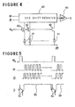
- In the above mentioned methods for driving the linear image sensor, the photodetectors are sequentially read out by the scanning circuit, and therefore, the noise is generated at each reading-out so that the noise cannot be sufficiently suppressed. In order to overcome the problem of the sequential reading of the photodetectors, there has been proposed and used a CCD linear image sensor as shown in Figure 4.
Photodetectors 41 which store electric charges of photosignals are connected throughtransfer gates 42 to respective stages of aCCD shift register 43. Thesetransfer gates 42 are simultaneously turned on by atransfer pulse 0□ as shown in Figure 5, so that a photosignal in eachphotodetector 41 are simultaneously transferred through the associatedgate 42 to the corresponding stage of aCCD shift register 43. Then, the photosignal in each stage of theCCD shift register 43 is serially transferred stage by stage by alternately supplying clock puIses ψ and ëj) as shown in Figure 5, so that a photosignal SP as shown in Figure 5 is outputted from theCCD shift register 43 to anoutput amplifier 44. - In the reading operation of the CCD image sensor as mentioned above, so-called "feed- through" noise Nf appear in the photosignal as shown in Figure 5. But, this niose is generated when the
transfer gates 42 are triggered. Therefore, the feed-through noise is a fixed pattern noise, and will not appear during the period of time for reading the photosignal of each scanning line from the CCD shift register. Accordingly, it is easy to remove the feed-through noises in a subsequent process of the signals. As seen from the above, the CCD image sensor is free from the fixed pattern noise, as generated in the MOSIC image sensor as shown in Figures 1 to 3. - In CCD image sensors recently developed, moreover, it is able to drive the CCD shift register at a transfer clock pulse frequency of 10 MHz or higher. If such a high speed CCD image sensor is applied to a contact type image sensor for A-4 size having 16 elements/mm resolution, namely, having 3456 photodetector cells, a reading speed of 0.4 msec/line or more can be expected. In addition, by alternately reading photodetector cells arranged in a line by use of a pair of CCD shift registers at a speed of 0.4 msec/line, a speed of 0.2 msec/line or more can be realized.
- Furthermore, if a so-called floating gate amplifier is used as the
output amplifier 44, the CCD image sensor can have an increased sensitivity, so that it can obtain an S/N ratio higher than the conventional MOSIC image sensor. - However, when there is fabricated a CCD linear image sesnor having for example 1728 or 3456 photodetector cells, since a CCD shift register chip having 1728 or 3456 stages is not commercially available, it is necessary to use a plurality of CCD shift register chips. In such a case, when a photosignal for one scanning line is read out by sequentially scanning the resepective CCD shift registers, the feed-through noise N, will inevitably appear at the boundary between the photosignal from one CCD shift register and the photosignal from the next CCD shift register. Therefore, a photosignal for one scanning line will inevitably contain several feed-through noise Nf.
- In addition, in the case that each of the CCD shift registers is provided at its output with one floating gate amplifier, if all the floating gate amplifiers are directly connected together to a common output line of the image sensor, a short- circuit situation is caused.
- Therefore, there is necessity for providing output terminals of the same number as the CCD shift registers used. For example, if each CCD shift register is of 256 stages, a contact type image sensor for A-4 size having 8 or 16 elements/mm resolution needs 7 or 14 output terminals. Such a CCD image sensor becomes complicated in wiring as compared with the MOSIC image sensor, resulting in poor reliability of connection to the external.
- Furthermore, the CCD image sensor has a problem of a so-called "image lag". Namely, when the photosignal is small, specifically when the voltage across the
photodetector 41 is not greater than 0.3V, even if thetransfer gate 42 is turned on, the electric charge will not be quickly and sufficiently be transferred from the photodetector to the CCD shift register. The voltage across the photodetector is determined by the amount of a photoelectric charge stored in the photodetector and the capacitance of the photodetector. Namely, the voltage across the photodetector is increased by increase of the amount of the photoelectric charge stored in the photodetector, but decreased by the capacitance of the photodetector. In addition, if the capacitance of the photodetector becomes larger than that of each stage of the CCD shift register, the amount of the electric charge transferred from the photodetector to the CCD shift register becomes small. - However, it is actually difficult to make 1 pF or less of capacitance of each photodetector including a capacitance of the associated distributing wire et al. On the other hand, in the case that a contact type image sensor for A-4 size having 16 elements/mm resolution and using a yellow green (wavelength 570 nm) LED having 100 1x in illuminance at the sensor surface is driven at the scanning speed of 1 msec/line, the photoelectric charge is merely about 0.2 pC per photodetector. As a result, the voltage across the photodetector will be only 200 mV. Additionally, the capacitance of the photodetector such as a-Si type photodetector cell is generally larger than that of the CCD type image sensor. Therefore, in the case that a-Si photodetectors are directly connected to the CCD shift register, the above mentioned image lag will occur, and therefore, a sufficient sensitivity cannot be obtained.
- It is, therefore, an object of the present invention to provide a contact type image sensor which is free from the problems as mentioned above.
- Another object of the present invention is to provide a low noise contact type image sensor capable of being driven at a high speed.
- A further object of the present invention is to provide a contact type linear image sensor which is free from the feed-through noise as mentioned above.
- Still another object of the present invention is to provide a contact type image sensor which has high abilities to obtain a higher scanning speed and a higher resolution than a MOSIC circuit and which can discriminate half tone.
- A still further object of the present invention is to provide a contact type image sensor using CCD driving circuit free of the aforementioned image lag.
- A further object of the present invention is to provide a method of driving such a sensor.
- The above and other objects of the present invention are accomplished according to a first aspect of the present invention by a contact type image sensor which comprises a plurality of photodetectors; a plurality of driving circuits each of which includes one charge shift register having a plurality of stages, an output amplifier connected to the output of the charge shift register, a change-over switch means connected to the output of the output amplifier, and a plurality of transfer gate means connected between respective stages of the charge shift register and the corresponding ones of the photodetectors in a one-to-one relation; and a common output line connected to the outputs of the change-over switch means of all the driving circuits.
- With the above arrangement, an electric charge in each of the photodetectors is transferred to the corresponding stage of the charge shift registers by turning on the transfer gate means. Thereafter, by applying transfer clock pulses to a selected one of the charge shift registers and turning on the change-over switch means associated the selected one charge shift register, photosignals temporarily stored in the selected one charge shift register are outputted through the associated output amplifier and the associated change-over switch means to the common output line.
- In one embodiment of the image sensor in accordance with the present invention, each of the transfer gate means of all the driving circuits has a controlled input connected in common to one control terminal. Preferably, each of the transfer gate means is a MOSFET having a gate connected in common to the one control terminal. In addition, the output amplifier of each driving circuit is a floating gate amplifier connected to the final stage of the associated charge shift register, and the change-over switch means of each driving circuit is a CMOS circuit. Furthermore, the charge shift registers are preferably formed by CTD shift registers such as CCD registers.
- In another embodiment of the image sensor, the charge shift registers are CCD shift registers, and each of the driving circuits further includes an auxiliary transfer gate means connected between each of the transfer gate means and the corresponding photodetector, and means for injecting bias charge to all the stages of the CCD shift register. With this arrangement, after the CCD shift register is injected with the bias charge, the transfer gate means and the auxiliary transfer gate means are simultaneously and twice turned on in such a manner that, upon the first turning-on, the bias charges in the CCD shift register are transferred to the corresponding photodetectors, and upon the second turning-on, the photoelectric charges plus the bias charges are transferred from the respective photodetectors to the corresponding stages of the CCD shift register.
- In this embodiment, preferably, each of the transfer gate means has a controlled input connected in common to a first control terminal, and each of the auxiliary transfer gate means has a controlled input connected in common to a second control terminal. In addition, each of the charge injection means includes a diode means connected to a voltage source, and an injection gate means connected between the diode means and the first stage of the associated CCD shift register.
- Furthermore, according to a second aspect of the present invention, there is provided a driving method for a contact type image sensor which includes a plurality of photodetectors; a plurality of driving circuits each of which includes one charge shift register having a plurality of stages, an output amplifier connected to the output of the charge shift register, a change-over switch means connected to the output of the output amplifier, and a plurality of transfer gate means connected between respective stages of the charge shift register and the corresponding ones of the photodetectors in a one-to-one relation; and a common output line connected to the output of the change-over switch means of all the driving circuits. This driving method includes the steps of simultaneously turning on the transfer gate means of all the driving circuits, so as to transfer an electric charge stored in each of the photodetectors to the corresponding stages of the charge shift registers; sequentially driving the charge shift registers one by one in the direction of arrangement of the photodetectors, by supplying transfer clock pulses only to a selected one of the charge shift registers and atthe same time turning on only the change-over switch means associated to the selected charge shift register during only the period of time in which the transfer pulses are applied; and repeatedly carrying out the above two steps.
- In the case that the charge shift registers are made of CCD shift registers, and each of the driving circuits further includes an auxiliary transfer gate means connected between each of the transfer gate means and the corresponding photodetector, and means for injecting bias charge to all the stages of the CCD shift register, the driving method for the image sensor additionally includes the steps of injecting the bias charge to the CCD shift register; and simultaneously turning on the transfer gate means and the auxiliary transfer gate means twice in such a manner that, upon the first turning-on, the bias charges in the CCD shift register are transferred to the corresponding photodetectors, and upon the second turning-on, the photoelectric charges plus the bias charges are transferred from the respective photodetectors to the corresponding stages of the CCD shift register.
- Preferably, each of the transfer gate means is a MOSFET whose gate is connected in common to a first control terminal, and each of the auxiliary transfer gate means is another MOSFET whose gate is connected in common to a second control terminal. In such a case, the first turning-on is carried out by applying a first gate pulse to the gate of the first MOSFET and at the same time supplying the gate of the second MOSFET with a second gate pulse having a voltage higher than that of the first gate pulse, and the second turning-on is carried out by simultaneously supplying the gates of the first and second MOSFETs with gate pulses of the voltages which are substantially the same as each other but lower than that of the second gate pulse.
- In addition, the charge injection means includes a diode means connected to a voltage source, and an injection gate means connected between the diode means and the first stage of the associated CCD shift register. With this arrangement, the injection of the bias charge to the CCD shift register is carried out by applying the injection gate means with injection gate pulses which are of the same number as that of the transfer pulses but are time-delayed from the transfer pulses by the length of time corresponding to one period of the transfer pulses, so that a bias charge is injected to the first stage of the CCD shift register and transferred stage by stage to the succeeding stages of the same CCD shift register in synchronism with the transfer of the photosignal through the same CCD shift register.
- The above and other objects, features and advantages of the present invention will become apparent from the following description taken in conjunction with the embodiments thereof with reference to the accompanying drawings.
-
- Figure 1 is a circuit diagram showing a basic construction of a contact type image sensor in the prior art;
- Figures 2 and 3 are circuit diagrams of MOSIC image sensor in the prior art in which the conventional noise suppression methods are carried out respectively;
- Figure 4 is a circuit diagram showing a basic construction of a CCD image sensor in the prior art;
- Figure 5 is a waveform diagram showing driving pulses for the CCD image sensor shown in Figure 4 and the output signal of the same sensor;
- Figure 6 is a circuit diagram showing a first preferred embodiment of a contact type CCD image sensor according to the present invention;
- Figure 7 is a time chart of various driving pulses for the CCD image sensor shown in Figure 6 and a waveform diagram of the output signal of the same sensor;
- Figure 8 is a circuit diagram showing a second preferred embodiment of a contact type CCD image sensor according to the present invention; and
- Figure 9 is a time chart of waveforms similar to Figure 7, but showing those for the image sensor shown in Figure 8.
- The present invention will be described in the following with reference to Figures 6 to 9, in which like Reference Numerals indicate like or corresponding components of the contact type CCD image sensor.
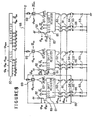
- Referring to Figure 6, a first preferred embodiment of the contact type CCD image sensor in accordance with the present invention comprises M integrated
circuit chips 60, each of which includes oneCCD shift register 61 formed on a semiconductor substrate and having N cascade- connected stages. For example, thisshift register 61 is a two-phase driven buried-channel type CCD shift register having a high transfer efficiency. By alternately supplying the two clock inputs of the respective CCD shift registers with first transfer clock pulses φ1~φM and second inverted transfer clock pulses φ1~φM from apulse generator 50, respectively, the electric charge stored in each stage in the CCD shift register is transferred stage by stage to the succeeding stages at each pair of first and second transfer clock pulses, with the result that the electric charge signal is serially outputted from an output terminal of each CCD shift register. - Each of the
stages 1...N of each CCD shift register is connected at its input to one transfer gate 52 constituted of for example one MOSFET as shown in Figure 6. Each of theMOSFET transfer gates 62 is connected to onephotodetector cell 63 through abonding pads bonding wire 66. Each of the photodetector cells is, for example, composed of an amorphous silicon film held between an individual metal electrode formed on an insulating substrate (not shown) such as glass and a common transparent electrode, so that all the photodetector cells are arranged in the form of one straight line. For example, the individual electrode is made of Au, and the common transparent electrode is made of ITO (Indium Tin Oxide). Thus, thetransfer gates 62 correspond to thephotodetector cell 63 in one-to-one relation, and therefore, by applying a transfer pulse (PG to all thetransfer gates 62, the electric charge stored in eachphotodetector 63 are simultaneously transferred through the associatedtransfer gate 62 to the corresponding stage of the CCD shift registers 61. - Furthermore, each of the CCD shift registers 61 is connected at its output to a floating
gate amplifier 67, whose output is connected to acommon output line 68 through an output change-overswitch 69 and abonding wire 70. Thisswitch 69 is constituted of for example a CMOS circuit which includes a pair of p-channel MOSFET and n-channel MOSFET turned on by a pair of gate pulses CPs and φs inverted in phase to each other. - In this way, each CCD driving
integrated circuit chip 60 comprises the N-stageCCD shift register 61, theN transfer gates 62, the floatinggate amplifier 67 and theswitch 69. The M chips 60 are assembled and attached on the substrate formed with the [NxM]photodetector cells 63. The gates of all theMOSFET transfer gates 62 in the M chips (i.e. [MxN] transfer gates) are connected in common to a control terminal, so that these gates are simultaneously turned on and off. Therefore, in the case that a contact type CCD image sensor for A-4 size and having 16 elements/mm resolution is fabricated by using CCD shift registers of 256 stages/chip, 14chips 60 have to be assembled on the substrate formed with 3456photodetectors 63. - The method of driving the aforementioned image sensor will then be described with reference to Figure 7.
- First, at the time ta, the transfer pulse φG is applied to all the
transfer gates 62, so that the transfer gates are turned on at the same time in order to simultaneously transfer the photoelectric charges stored in all thephotodetectors 63 to the corresponding stages of all the CCD shift registers 61. - After a predetermined time has elapsed from the falling time t, of the transfer pulse (PG to allow the feed-through noise Nf to disappear, the transfer clock pulses φ1 and $1 are applied to only the first
CCD shift register 61 so as to transfer the charges in the respective stages of thefirst register 61 to the succeeding stages, stage by stage. The photoelectric charge in each stage is transferred one stage by one pair of clock pulses φ1 and φ1' and therefore, N pairs of clock pulses φ1 and φ1 are applied to theCCD shift register 61, so that all the photoelectric charges temporarily stored in the first to Nth stages of the firstCCD shift register 61 are sequentially outputted to the associated floatinggate amplifier 67. - On the other hand, the gate pulses φs1 and φs1 are applied to the output change-over
switch 69 of the firstCCD shift register 60 so that theswitch 69 is turned on. The gate pulse φs1 has a high level period corresponding to the period of time in which the N clock pulses φ1, are sequentially applied, and the gate pulse φs1 is reverse in phase to the gate pulse φs1. However, no gate pulse is applied to theswitches 69 of the second to Nth CCD shift registers 61, so that these switches are kept in an OFF state. Thus, the photoelectric charges in the respective stages of the firstCCD shift register 61 are sequentially outputted through theswitch 69 to thecommon output line 68, but, the photoelectric charges stored in all theregisters 60 except the first one are not transferred and remain stored there in the period of time tS1―tS2. - After the readout of the output signals of the first
CCD shift register 61, the transfer clock pulses φ2 and $2 are then applied to the secondCCD shift register 61 and the output change-overswitch 69 associated to the second CCD register is turned on by the gate pulses φS2 and φS2. Neither the transfer clock pulses nor the gate pulses are applied to theCCD shift registers 61 excluding the second one. Therefore, the photosignal stored in thesecond CCD register 61 are sequentially transferred and then outputted to theoutput line 68. - Hereinafter, the same operations are sequentially practiced on the third CCD shift register to the Mth CCD register in order.
- Thus, the photoelectric charges in the [NxM]
photodetectors 63 are successively read out, so that the photosignal as shown in Figure 7 are outputted to thecommon output line 68. - In this first preferred embodiment, each
transfer gate 62 is turned on only once during a scanning time for each one line, but out of the period tS1~tSM +1 of reading photosignals from the CCD shift registers. Therefore, the feed-through nioses N, caused by triggering thetransfer gates 62 will not be contained in the photosignals outputted through theoutput line 68. In this connection, another feed-through noises will be generated by the pulses φS1~φSM and φS1~φSM applied to the output change-over switches 69. But, this is negligible, because such feedthrough noise will in general be not greater than 1 mV, and on the other hand, the photosignals are amplified by the floatinggate amplifiers 63 to have a value of about 1 V for example. - In place of CMOS switch, a MOS switch of P-channel or N-channel can be used as an output change-over
switch 69. However, the CMOS switch has the advantage capable of cancelling the noises by a pair of positive and negative pulses, as mentioned hereinbefore. - When one change-
over switch 69 on one chip is in ON-state, theswitches 69 on the other chips are in OFF-state. Any short circuit is not, therefore, caused even if the outputs of all the floating gate amplifiers are connected thecommon output line 68. As the result, there is no necessity for providing more than one output line for one contact type image sensor. - In the aforementioned CCD contact type linear image sensor, the photoelectric charge stored in each photodetector is intermittently transferred to the CCD shift register. Therefore, the charge given by a dark current is stored in the CCD shift register during a period of time from the moment the transfer of charge from at CCD shift register has been completed to the moment the next transfer of charge from the same CCD shift register is started. In this embodiment, however, such a dark charge does not become a substantial cause of noise to the photosignal.
- For example, in case of a contact type image sensor for A-4 size having 16 elements/mm resolution and driven at 1 msec/line scanning speed, the photoelectric charge of about 0.2 pC is stored under illumination of 100 1x (wavelength 555 nm) and the photodetector aperture size of 0.05x0.06 mm2. On the other hand, the dark charge stored in the
CCD shift register 61 is about 1 x 1 0-4 pC at the scanning speed of 1 msec/line. Therefore, the noise caused by the dark charge is negligible since this dark charge is extremely smaller than the photoelectric charge. - Referring to Figure 8, there is shown a second preferred embodiment of the CCD contact type linear image sensor in accordance with the present invention. This second embodiment is an improvement to the first embodiment, and therefore, components similar to those of the first embodiment shown in Figure 6 are given the same Reference Numerals. Namely, the second embodiment also comprises M photodetector reading-out
IC chip 60 each of which includes an N stageCCD shift register 61 having an output connected through a floatinggate amplifier 67 and a CMOS type change-over switch 69 to acommon output line 68. Each stage of theCCD shift register 61 is connected to the corresponding onephotodetector 63 thorugh onetransfer gate 62, thebonding pad 64, thebonding wire 66 and thebonding pad 65. - In this second embodiment, an
anxiliary transfer gate 81 is connected between eachtransfer gate 62 and the associatedbonding pad 64. Thisauxiliary gate 81 is constituted of one MOSFET, similarly to thetransfer gate 62. Moreover, adiode 82 is connected through anothertransfer gate 83 to the first stage of eachCCD shift register 61. Thisdiode 82 is reversely biased to constitute a capacitor as shown in Figure 8, and a potential cp,, is applied to a connection node between thediode 82 and the associatedtransfer gate 83. Therefore, by turning on thetransfer gate 83, a bias charge is injected from thediode capacitor 82 through thetransfer gate 83 to the first stage of theCCD shift register 60. - Similarly to the first embodiment shown in Figure 6, one N-stage
CCD shift register 61, N pairs oftransfer gates 62 andauxiliary gates 81, one floatinggate amplifier 67, oneswitch 69, onediode 82 and onetransfer gate 83 are manufactured on asingle IC chip 60. The M chips 60 are assembled and attached on the substrate formed with the [NxM]photodetectors 63. The gates of all the transfer gates 62 (i.e. [M x N] transfer gates) are connected in common so that all the transfer gates are simultaneously turned on and off. Also, the gates ofauxiliary gates 81 are connected in common, so that all the MxN auxiliary gates are turned on and off at one time. In addition, in the case that a contact type CCD image sensor for A-4 size and having 16 elements/mm resolution is fabricated by using CCD shift registers of 256 stages/chip, 14chips 60 have to be assembled on the substrate formed with 3456photodetectors 63. - The image sensor as mentioned above is operated as follows:
- In the condition that the
CCD shift registers 60 are precharged in the manner as explained hereinafter, theMxN transfer gates 62 and the MxNauxiliary gates 81 are simultaneously turned on twice in succession by the transfer gate pulse (PTG and the auxiliary gate pulse φPG as shown in Figure 9. - Specifically at the first turning-on time,
transfer gates 62 and theauxiliary gates 81 are simultaneously turned on, but theauxiliary gates 81 are applied with a gate voltage φPG higher than that φTG applied to thetransfer gates 62 as shown in Figure 9, so that there is produced such an inclined potential distribution that the potential is the highest under the gate of the CCD shift register and is lowered step by step toward the transfer gate and the auxiliary gate and then becomes the lowest under the photodetector. Accordingly, the bias charge stored in each stage of the CCD shift register is transferred or injected to the associated photodetector, with the result that the photoelectric charge plus the bias charge is stored in the photodetector. - At the second turning-on time, the
transfer gates 62 and theauxiliary gates 81 are applied with the same gate voltages (PTG and φPG as shown in Figure 9, resulting in production of such a potential distribution that the potential is the highest under the photodetector and is lowered at the auxiliary gate and the transfer gate and then becomes the lowest under the gate of the CCD shift register. Thus, the photoelectric charge plus the bias charge in the respective photodetector is transferred to the corresponding stage of the CCD shift register. - Namely, even if the photosignal voltage across the photodetector is very small, since the photosignal voltage is increased with a bias voltage as mentioned above, the photosignal voltage is quickly and surely transferred from the photodetector to the CCD shift register when the transfer gate and the auxiliary gate are turned on. This CCD image sensor is free from the problem of the persistence of charge mentioned hereinbefore caused by a small quantity of photoelectric charge stored in the photodetector.
- Thereafter, the transfer clock pulses φ1 as shown in Figure 9 and the inverted transfer clock pulses φ1 are applied to only the first
CCD shift register 61 so as to transfer the charges in the respective stages of thesame register 61 to the succeeding stages, stage by stage, and to finally output the photosignal from the output terminal to theamplifier 67. At the same time, the gate pulse φS1, shown in Figure 9 and the inverted gate pulse φS1 are applied to the output change-overswitch 69 of the firstCCD shift register 61 so that the switch is turned on during the period of time in which the transfer clock pulses φ1 and ii> are applied. Thus, the photoelectric charges in the respective stages of the firstCCD shift register 61 are sequentially outputted through theswitch 69 to thecommon output line 68. - At this time, injection gate pulses φIG1 as shown in Figure 9 are applied to the
injection gate 83 connected to the input of the firstCCD shift register 61. With intermittent turning-on of theinjection gate 83, the charge stored in thecapacitor 82 applied with a constant voltage φIB from thepulse generator 50 is intermittently injected to the first stage of the firstCCD shift register 61. Such an injected charge will be transferred to the next stage is synchronism with the transfer of the photosignal through the CCD shift register. In order to cause all the N stages of the CCD shift register to store the injected charge, N injection gate pulses φIG1 are applied to thegate 83, but have to be delayed from the transfer clock pulses φ1 by one period of the transfer pulse (pl, so that the injected bias charge will not be superimposed with the photoelectric charge being transferred through the CCD shift register. Thus, substantially simultaneously with the completion of the transfer of the photoelectric charge from the firstCCD shift register 61, the new bias charge for the next scanning line are stored in each stage of the firstCCD shift register 61. - During the aforementioned operation in the first
CCD shift register 61 for the photosignal transfer and the injection of the bias charge, the photoelectric charges (plus the bias charges) stored in the CCD shift registers other than the first one will not be transferred and remain stored, similarly to the first embodiment. - After the readout of the photosignals of the
first CCD register 61, the transfer clock pulses φ2 and CP2 are then applied to the secondCCD shift register 61 and the output change-overswitch 64 associated to the secondCCD shift register 61 is turned on by the gate pulses φS2 and φS2. On the other hand, the injection gate pulses φIG2 are applied to theinjection gate 83 connected to the input of the secondCCD shift register 61. Therefore, the photosignal stored in the respective stages of the secondCCD shift register 61 are sequentially transferred through the secondCCD shift register 61 and finally outputted through theamplifier 67 to thecommon output line 68, and at the same time, the new bias charge for the next scanning line are stored in the secondCCD shift register 61. - Hereinafter, the same operations are sequentially practiced on the third to the Mth CCD shift registers in order.
- In this way, the photoelectric charges including the bias charges as shown in Figure 9 are outputted from an output O of the contact type image sensor. Since these bias charges are regarded as DC offset, it is easy to remove the bias charge component in a subsequent process of the signals. Only real photosignals can therefore be obtained.
- In this second embodiment, since the photoelectric charges are added with the biasing charges, the voltage across the
photodetector 63 becomes higher, with the result that the aforementioned "image lag" is overcame. This bias charge is sufficient if it is of about 0.3 pC. In such a case, if the photoelectric charge stored in each photodetector cell is of about 0.2 pC as mentioned above, the total charge will be of about 0.5 pC. This total charge can be transferred without overflow in a shift register having cell size of 15x30 pM 2 which is often used in CCD recently. - Incidentally, for the purpose of simplification of the drawings, electric power lines and ground lines are omitted. Therefore, it should be understood that the CCD image sensors shown in Figures 6 and 8 includes power lines, ground lines, etc, which are required in the matter of course in an integrated circuit.
- As will be apparent from the above explanation, the contact type CCD image sensor constructed and operated in accordance with the present invention can realize a high scanning speed at a very low noise, since the photoelectric charges in all the photodetectors are simultaneously transferred to a plurality of CCD shift registers which are inherently low in noise characteristics, and then, the photoelectric charges temporarily stored in the CCD shift registers are read out in such a manner that there is omitted the feed-through noise caused at the time of transferring the charge from the photodetectors to the CCD shift register. For example, in case of a contact type image sensor for A-4 size having 16 elements/mm resolution, a S/N ratio of not less than 40 dB can be obtained at a scanning speed of 0.5 msec/line, and therefore, a half tone image can be sufficiently detected or discriminated.
- In addition, the image sensor has only one output line. Accordingly, the image sensor can be simply connected to an external circuit, and since only one signal line is required for connection to an external, the reliability in signal transmission to an external will be high.
- Furthermore, and as another important advantage of the present invention, the image sensor is very improved in sensitivity by injecting the bias charge to the photodetectors before transferring the photoelectric charge from each photodetector to the CCD shift registers. Namely, since the amount of charge in the photodetector is increased by such an injection of the bias charge, the voltage across the photodetector becomes high, and therefore, the difference in potential between the CCD shift register and the photodetector also becomes large. Accordingly, a substantial amount of charge can be quickly and surely transferred from the photodetector to the shift register, with the result that there is overcome the persistence of charge which is caused because of the capacitance of the photodetectors larger than that of the CCD shift register and because of a relatively small amount of photoelectric charge stored in the photodetector even if the exposure to the photodetector is at maximum. The bias charges are injected or stored into the stages of the CCD shift register, concurrently with the reading-out of the photosignalsfrom the CCD shift register, and the bias charges are simultaneously injected from the respective stages of the CCD shift registers to the corresponding photodetectors. Therefore, the contact type image sensor can have a very high S/N ratio without lowering the scanning speed.
- While the invention has been particularly shown and described with reference to preferred embodiments thereof, it will be understood by those skilled in the art that the foregoing and other changes in form and details can be made without departing from the scope of the invention.
Claims (15)
Applications Claiming Priority (4)
| Application Number | Priority Date | Filing Date | Title |
|---|---|---|---|
| JP143020/84 | 1984-07-10 | ||
| JP59143020A JPS6121669A (en) | 1984-07-10 | 1984-07-10 | Contact sensor and its driving method |
| JP59164445A JPH0666851B2 (en) | 1984-08-06 | 1984-08-06 | Contact image sensor |
| JP164445/84 | 1984-08-06 |
Publications (3)
| Publication Number | Publication Date |
|---|---|
| EP0168030A2 EP0168030A2 (en) | 1986-01-15 |
| EP0168030A3 EP0168030A3 (en) | 1987-08-05 |
| EP0168030B1 true EP0168030B1 (en) | 1990-09-26 |
Family
ID=26474847
Family Applications (1)
| Application Number | Title | Priority Date | Filing Date |
|---|---|---|---|
| EP85108514A Expired - Lifetime EP0168030B1 (en) | 1984-07-10 | 1985-07-09 | Contact type image sensor and driving method therefor |
Country Status (3)
| Country | Link |
|---|---|
| US (1) | US4672453A (en) |
| EP (1) | EP0168030B1 (en) |
| DE (1) | DE3579854D1 (en) |
Families Citing this family (28)
| Publication number | Priority date | Publication date | Assignee | Title |
|---|---|---|---|---|
| DE69027346T2 (en) * | 1989-02-10 | 1996-10-31 | Canon Kk | Sensor chip and this photoelectric conversion device using it |
| JP2654167B2 (en) * | 1989-02-28 | 1997-09-17 | キヤノン株式会社 | Photoelectric conversion device |
| JPH03119855A (en) * | 1989-10-02 | 1991-05-22 | Nippon Steel Corp | Contact type image sensor |
| US5103322A (en) * | 1990-05-14 | 1992-04-07 | Polaroid Corporation | Scanner with retractable roller feed |
| US5111263A (en) * | 1991-02-08 | 1992-05-05 | Eastman Kodak Company | Charge-coupled device (CCD) image sensor operable in either interlace or non-interlace mode |
| US5299013A (en) * | 1991-07-25 | 1994-03-29 | Dyna Image Corp. | Silicon butting contact image sensor with two-phase shift register |
| JP2910485B2 (en) * | 1993-02-19 | 1999-06-23 | 富士ゼロックス株式会社 | Image reading apparatus and image reading method |
| US5543838A (en) * | 1993-08-31 | 1996-08-06 | Xerox Corporation | Signal multiplexing system for an image sensor array |
| AU6899896A (en) * | 1995-08-21 | 1997-03-27 | Starcam Systems, Inc. | High-speed high-resolution multi-frame real-time digital camera |
| US5760833A (en) * | 1996-05-20 | 1998-06-02 | Torrey Science Corporation | Readout of pixel data from array of CCD image detectors |
| US6219468B1 (en) * | 1996-10-17 | 2001-04-17 | Minolta Co., Ltd. | Image detection system |
| US6786420B1 (en) | 1997-07-15 | 2004-09-07 | Silverbrook Research Pty. Ltd. | Data distribution mechanism in the form of ink dots on cards |
| US6618117B2 (en) | 1997-07-12 | 2003-09-09 | Silverbrook Research Pty Ltd | Image sensing apparatus including a microcontroller |
| US6948794B2 (en) | 1997-07-15 | 2005-09-27 | Silverbrook Reserach Pty Ltd | Printhead re-capping assembly for a print and demand digital camera system |
| US7110024B1 (en) | 1997-07-15 | 2006-09-19 | Silverbrook Research Pty Ltd | Digital camera system having motion deblurring means |
| US6624848B1 (en) | 1997-07-15 | 2003-09-23 | Silverbrook Research Pty Ltd | Cascading image modification using multiple digital cameras incorporating image processing |
| US6690419B1 (en) | 1997-07-15 | 2004-02-10 | Silverbrook Research Pty Ltd | Utilising eye detection methods for image processing in a digital image camera |
| US6879341B1 (en) | 1997-07-15 | 2005-04-12 | Silverbrook Research Pty Ltd | Digital camera system containing a VLIW vector processor |
| SG70128A1 (en) * | 1997-10-06 | 2000-01-25 | Canon Kk | Method of driving image sensor |
| AUPP702098A0 (en) | 1998-11-09 | 1998-12-03 | Silverbrook Research Pty Ltd | Image creation method and apparatus (ART73) |
| KR100430099B1 (en) * | 1999-03-02 | 2004-05-03 | 엘지.필립스 엘시디 주식회사 | Shift Register Circuit |
| AUPQ056099A0 (en) | 1999-05-25 | 1999-06-17 | Silverbrook Research Pty Ltd | A method and apparatus (pprint01) |
| US7334791B2 (en) * | 2002-08-24 | 2008-02-26 | Blinky Bones, Inc. | Electronic die |
| US20050231621A1 (en) * | 2004-04-20 | 2005-10-20 | Su Wen H | Integrated image detecting apparatus |
| JP4120890B2 (en) * | 2005-06-30 | 2008-07-16 | ブラザー工業株式会社 | Image reading device |
| US20090228463A1 (en) * | 2008-03-10 | 2009-09-10 | Cramer Richard D | Method for Searching Compound Databases Using Topomeric Shape Descriptors and Pharmacophoric Features Identified by a Comparative Molecular Field Analysis (CoMFA) Utilizing Topomeric Alignment of Molecular Fragments |
| US10090349B2 (en) * | 2012-08-09 | 2018-10-02 | Taiwan Semiconductor Manufacturing Company, Ltd. | CMOS image sensor chips with stacked scheme and methods for forming the same |
| JP6516204B2 (en) * | 2016-01-19 | 2019-05-22 | 京セラドキュメントソリューションズ株式会社 | Image reading apparatus, image reading method, image forming apparatus and control program |
Family Cites Families (5)
| Publication number | Priority date | Publication date | Assignee | Title |
|---|---|---|---|---|
| JPS564946A (en) * | 1979-05-24 | 1981-01-19 | Nec Corp | Speed converter using charge transfer device |
| JPS5780864A (en) * | 1980-11-08 | 1982-05-20 | Hitachi Ltd | Driving circuit for ccd photosensor |
| JPS58125952A (en) * | 1982-01-22 | 1983-07-27 | Fuji Xerox Co Ltd | Original reader |
| JPS59160374A (en) * | 1983-03-02 | 1984-09-11 | Canon Inc | Photoelectric converter |
| US4620231A (en) * | 1984-06-18 | 1986-10-28 | Rca Corporation | CCD imager with photodetector bias introduced via the CCD register |
-
1985
- 1985-07-09 DE DE8585108514T patent/DE3579854D1/en not_active Expired - Fee Related
- 1985-07-09 US US06/753,232 patent/US4672453A/en not_active Expired - Fee Related
- 1985-07-09 EP EP85108514A patent/EP0168030B1/en not_active Expired - Lifetime
Also Published As
| Publication number | Publication date |
|---|---|
| US4672453A (en) | 1987-06-09 |
| EP0168030A3 (en) | 1987-08-05 |
| EP0168030A2 (en) | 1986-01-15 |
| DE3579854D1 (en) | 1990-10-31 |
Similar Documents
| Publication | Publication Date | Title |
|---|---|---|
| EP0168030B1 (en) | Contact type image sensor and driving method therefor | |
| US9490291B2 (en) | Solid state imaging device and camera system | |
| US3946151A (en) | Semiconductor image sensor | |
| EP1178673B1 (en) | Solid state image pickup apparatus | |
| EP0272152B1 (en) | Signal reading out circuit | |
| US4189749A (en) | Solid state image sensing device | |
| EP1178674B1 (en) | Solid-state image pickup device and camera system | |
| US6674471B1 (en) | Solid-state imaging device and method for driving the same | |
| US4450484A (en) | Solid states image sensor array having circuit for suppressing image blooming and smear | |
| US4366503A (en) | Solid state image pick-up device and its charge transfer method | |
| EP0548987B1 (en) | Source follower circuit for image sensor | |
| EP0577391B1 (en) | Solid state image pickup apparatus | |
| US6980243B2 (en) | Photoelectric conversion device providing advantageous readout of two-dimensional array of transistors | |
| US4413283A (en) | Solid-state imaging device | |
| US4609825A (en) | Device for modulating the sensitivity of a line-transfer photosensitive device | |
| US6657664B2 (en) | Solid-state image pickup device | |
| JPH0462225B2 (en) | ||
| US5831675A (en) | Solid state imaging device | |
| JP2000152090A (en) | Solid-state image pickup device | |
| JPH10200817A (en) | Solid-state image pickup device | |
| JPS60172A (en) | Solid-state image pickup device | |
| JPH0666851B2 (en) | Contact image sensor | |
| JPH09247355A (en) | Image sensor and image sensor unit using the sensor | |
| JPS6121669A (en) | Contact sensor and its driving method | |
| JPS63232761A (en) | Signal transferring device |
Legal Events
| Date | Code | Title | Description |
|---|---|---|---|
| PUAI | Public reference made under article 153(3) epc to a published international application that has entered the european phase |
Free format text: ORIGINAL CODE: 0009012 |
|
| 17P | Request for examination filed |
Effective date: 19850709 |
|
| AK | Designated contracting states |
Designated state(s): DE FR GB NL |
|
| PUAL | Search report despatched |
Free format text: ORIGINAL CODE: 0009013 |
|
| RHK1 | Main classification (correction) |
Ipc: H04N 1/04 |
|
| AK | Designated contracting states |
Kind code of ref document: A3 Designated state(s): DE FR GB NL |
|
| 17Q | First examination report despatched |
Effective date: 19891222 |
|
| GRAA | (expected) grant |
Free format text: ORIGINAL CODE: 0009210 |
|
| AK | Designated contracting states |
Kind code of ref document: B1 Designated state(s): DE FR GB NL |
|
| REF | Corresponds to: |
Ref document number: 3579854 Country of ref document: DE Date of ref document: 19901031 |
|
| ET | Fr: translation filed | ||
| PLBE | No opposition filed within time limit |
Free format text: ORIGINAL CODE: 0009261 |
|
| STAA | Information on the status of an ep patent application or granted ep patent |
Free format text: STATUS: NO OPPOSITION FILED WITHIN TIME LIMIT |
|
| 26N | No opposition filed | ||
| PGFP | Annual fee paid to national office [announced via postgrant information from national office to epo] |
Ref country code: GB Payment date: 19950703 Year of fee payment: 11 |
|
| PGFP | Annual fee paid to national office [announced via postgrant information from national office to epo] |
Ref country code: FR Payment date: 19950725 Year of fee payment: 11 |
|
| PGFP | Annual fee paid to national office [announced via postgrant information from national office to epo] |
Ref country code: NL Payment date: 19950728 Year of fee payment: 11 |
|
| PGFP | Annual fee paid to national office [announced via postgrant information from national office to epo] |
Ref country code: DE Payment date: 19950920 Year of fee payment: 11 |
|
| PG25 | Lapsed in a contracting state [announced via postgrant information from national office to epo] |
Ref country code: GB Effective date: 19960709 |
|
| PG25 | Lapsed in a contracting state [announced via postgrant information from national office to epo] |
Ref country code: NL Effective date: 19970201 |
|
| GBPC | Gb: european patent ceased through non-payment of renewal fee |
Effective date: 19960709 |
|
| PG25 | Lapsed in a contracting state [announced via postgrant information from national office to epo] |
Ref country code: FR Effective date: 19970328 |
|
| NLV4 | Nl: lapsed or anulled due to non-payment of the annual fee |
Effective date: 19970201 |
|
| PG25 | Lapsed in a contracting state [announced via postgrant information from national office to epo] |
Ref country code: DE Effective date: 19970402 |
|
| REG | Reference to a national code |
Ref country code: FR Ref legal event code: ST |