EP0158219B1 - Sync responsive clock generator for digital demodulators - Google Patents
Sync responsive clock generator for digital demodulators Download PDFInfo
- Publication number
- EP0158219B1 EP0158219B1 EP85103614A EP85103614A EP0158219B1 EP 0158219 B1 EP0158219 B1 EP 0158219B1 EP 85103614 A EP85103614 A EP 85103614A EP 85103614 A EP85103614 A EP 85103614A EP 0158219 B1 EP0158219 B1 EP 0158219B1
- Authority
- EP
- European Patent Office
- Prior art keywords
- pulse
- generating
- clock
- output
- frequency
- Prior art date
- Legal status (The legal status is an assumption and is not a legal conclusion. Google has not performed a legal analysis and makes no representation as to the accuracy of the status listed.)
- Expired
Links
Images


Classifications
-
- G—PHYSICS
- G11—INFORMATION STORAGE
- G11B—INFORMATION STORAGE BASED ON RELATIVE MOVEMENT BETWEEN RECORD CARRIER AND TRANSDUCER
- G11B20/00—Signal processing not specific to the method of recording or reproducing; Circuits therefor
- G11B20/10—Digital recording or reproducing
- G11B20/14—Digital recording or reproducing using self-clocking codes
- G11B20/1403—Digital recording or reproducing using self-clocking codes characterised by the use of two levels
- G11B20/1423—Code representation depending on subsequent bits, e.g. delay modulation, double density code, Miller code
- G11B20/1426—Code representation depending on subsequent bits, e.g. delay modulation, double density code, Miller code conversion to or from block codes or representations thereof
-
- G—PHYSICS
- G11—INFORMATION STORAGE
- G11B—INFORMATION STORAGE BASED ON RELATIVE MOVEMENT BETWEEN RECORD CARRIER AND TRANSDUCER
- G11B20/00—Signal processing not specific to the method of recording or reproducing; Circuits therefor
- G11B20/10—Digital recording or reproducing
- G11B20/14—Digital recording or reproducing using self-clocking codes
- G11B20/1403—Digital recording or reproducing using self-clocking codes characterised by the use of two levels
- G11B20/1423—Code representation depending on subsequent bits, e.g. delay modulation, double density code, Miller code
- G11B20/1426—Code representation depending on subsequent bits, e.g. delay modulation, double density code, Miller code conversion to or from block codes or representations thereof
- G11B2020/1461—8 to 14 modulation, e.g. the EFM code used on CDs or mini-discs
Description
- The present invention relates to a clock generator according to the preamble of claim 1. A clock generator of this kind is suitable for deriving clock information from a digital bit stream.
- In compact disc recording a digital modulation technique, known as eight-to-fourteen modulation (EFM), is employed whereby original eight bit codes of random clock spacings are converted to fourteen bit codes of the format having a minimum spacing of three clock pulses and a maximum spacing of eleven clock pulses to provide enough tracking information for laser beam to follow tracks and enough clock information for disc players to demodulate the EFM bit stream. The fourteen-bit codes are formatted into a series of data blocks, or "frames" each being identified by a 24-bit frame sync code composed of consecutive series of eleven bits of "1"s and eleven bits of "0"s plus two binary "1"s.
- Conventional clock generators employed in compact disc players include circuitry for detecting a series of data bits having the minimum and maximum clock spacings and counting clock pulses generated by a voltage-controlled oscillator which are present during the minimum and maximum spacings of the detected data bits. Two count values are derived as a measure of the frequency of the clock pulse and used to control the operating frequency of the oscillator. One disadvantage of the prior art is that it requires many circuit components with a resultant increase in cost. Another disadvantage resides in the fact that since the data bits of minimum and maximum clock spacings occur at random, the phase-locked loop is likely to remain out-of-phase with the input bit stream for a substantial period if successive frames contain no data bits having minimum and maximum clock spacings.
- In EP-A-74 793 a clock generator comprising the features stated in the preamble of claim 1 is shown. The known clock generator includes a phase-locked loop circuit for synchronizing the clock frequency of an internal voltage-controlled oscillator with the bit rate of incoming signals. In the known circuit two frequency phase comparators and a phase comparator are provided, one of the frequency phase comparators comparing the input data stream with the output signal of the voltage-controlled oscillator, while the second frequency phase comparator compares the output signal of a crystal oscillator with the output signal of the voltage-controlled oscillator. As an alternative, only one frequency phase comparator comparing the output signal of the voltage-controlled oscillator with the input data stream is provided in addition to the phase comparator. In the known circuit a synchronization signal detector is also provided which transmits the output signal of the frequency phase comparator for the control of the voltage-controlled oscillator when the synchronization signal portion is detected, while it transmits the output signal of the phase comparator for the control of the voltage-controlled oscillator when the data portion is received.
- From EP-A-96 106, a phase-locked circuit is known in which a detector for detecting the maximum inverting period value in an EFM input signal is provided. Furthermore, a phase comparator is provided which compares the phase of the output signal of a voltage-controlled oscillator with the phase of the EFM input signal. The output signals of the phase comparator and of the detector are combined via an adder and then serve to control the voltage-controlled oscillator on the frequency of the EFM input signal.
- It is an object of the present invention to provide a clock generator which is simple in circuit design and stable in clock frequency.
- This object is obtained by the features stated in claim 1.
- The clock generator of the invention is adapted to receive a bit stream of a frame format having a frame sync and derives a frequency control signal from the frame sync of the input bit stream.
- The proposed clock generator comprises a voltage-controlled oscillator for generating clock pulses, means for generating a window pulse in response to a predetermined transition between binary "1"s and binary "0"s in the bit stream, a phase comparator responsive to the window and clock pulses for generating a phase control signal representing the difference in phase between the window pulse and the clock pulse, and a frequency comparator. The frequency comparator is responsive to the bit stream and the clock pulses to detect the synchronization code and the number of clock pulses present during the period of the detected synchronization code and to generate a frequency control signal of different levels according to the detected number of clock pulses. The phase and frequency control signals are combined and applied to the voltage-controlled oscillator to control the phase and frequency of the clock pulses.
- The periodicity of the frame sync allows the clock generator to quickly return to phase-locked state as soon as the clock frequency deviates from the normal frequency value. Since it is only required to detect the sync code for frequency control, the circuitry is simpler than that of the prior art.
- The invention is particularly suitable for demodulating an eight-to-fourteen modulation (EFM) bit stream which is derived from digital audio discs such as "compact discs".
- The present invention will be described in further detail with reference to the accompanying drawings, in which:
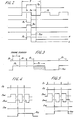
- Fig. 1A is a block diagram of a phase-locked loop of the invention;
- Fig. 1 is a block diagram of a frequency comparator constructed according to the invention;
- Fig. 1C is an illustration of a modified form of the frequency comparator;
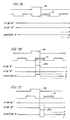
- Fig. 2 is a waveform diagram useful for describing the operation of the phase-locked loop;
- Figs. 3 and 4 are waveform diagrams useful for describing the operation of the frequency comparator of Fig. 1B, and Fig. 5 is a waveform diagram useful for describing the operation of the frequency comparator of Fig. 1C;
- Fig. 6 is a block diagram of a modified phase-locked loop of the invention; and
- Figs. 7A to 7C are waveform diagrams associated with the block diagram of Fig. 6.
- In Figs. 1A and 2B, there is shown a preferred embodiment of the clock generator of the present invention. The clock generator comprises a phase-locked
loop 10 shown in Fig. 1A and afrequency comparator 12 shown separately in Fig. 1B. The phase-lockedloop 10 includes awindow pulse generator 13, aphase comparator 14, areference circuit 15,noise suppressors differential integrator 18 and a voltage controlledoscillator 19.Window pulse generator 13 is connected to aninput terminal 20 to which a digitally modulated bit stream is applied. - The input signal is derived from a digital audio disc known as compact disc, in which the original 16-bit digital sample of 44.1 kHz is subjected to eight-to-fourteen modulation (EFM). According to this digital modulation, the original 16 bit code is divided into upper and lower binary significant groups of eight bits each and each group is converted to a 14-bit code in which binary "1"s occur at calculated maximum intervals to make it less likely to lose clock timing on playback. The EFM modulated bit stream is formatted into a series of data blocks, or frames of 588 bits, each identified by a 24-bit frame sync code. The frame sync code comprises a succession of eleven bits of "1"s and eleven bits of "0"s followed by two bits "1"s at the beginning of each frame. The frame sync code is followed by a data bit stream in which binary "1"s occur at a minimum spacing of 3 clock intervals and at a maximum spacing of 11 clock intervals. Binary "1"s and binary "0"s in the input bit stream present high and low voltages, respectively, at the
input terminal 20. The frame sync code forms a consecutive train of a positive-going pulse of 11-clock period and a negative-going pulse of the same period and the data bits form a series of randomly occurring positive-going pulses. - The
window pulse generator 13 is responsive to the transition of binary level that occurs at the rising edge and/or falling edge of the positive-going pulses of the input bit stream and generates a window pulse Pw of a duration Tw smaller than the pulse spacing T of clock pulses Pc generated by the voltage controlledoscillator 19. The waveforms of these pulses are shown at Fig. 2. Preferably, the window and clock pulses have equal pulse duration. - The
phase comparator 14 comprises aNAND gate 21, Exclusive-OR gates resistors resistors OR gates NAND gate 21 and the other input of Exclusive-ORgate 22 is connected to logical high level source. The other input ofgate 23 is connected to the output ofwindow pulse generator 13. A junction betweenresistors resistors noise suppressor 16 to the inverting input of anoperational amplifier 30.Resistors OR gates junction A. Resistors - Window pulses are supplied to one input of
NAND gate 21 to be compared in phase with clock pulses from theoscillator 19. The phase difference between these pulses results in the generation of a negative-going pulse Pn whose leading edge is coincident with the leading edge of window pulse Pw and whose trailing edge is coincident with the trailing edge of clock pulse Pc, as shown in Fig. 2. - Exclusive-OR
gate 22 provides a first, positive-going phase error pulse Pe1 which is reverse in polarity to the input pulse Pn. Exclusive-ORgate 23 provides a second, negative-going phase error pulse Pe2 whose leading edge is coincident with the trailing edge of clock pulse Pc and whose trailing edge is coincident with the trailing edge of window pulse Pw. The durations of phase error pulses Pe1 and Pe2 thus vary complementafily with each other according to the amount of phase difference between pulses Pw and Pc. The positive-going pulse Pe1 and negative-going pulse Pe2 are combined at junction A so that the potential thereat is driven to a high voltage level H in the presence of the pulse Pe1 and driven to a lower voltage level L in the presence of the pulse Pe2 for complemental periods of time as shown at Pe in Fig. 2 on detection of a phase difference. -
Noise suppressor 16 is formed by a pair of antiparallel-connecteddiodes 28 and 29. The phase error voltage having amplitudes greater than the thresholds ofdiodes 28 and 29 is passed to the inverting input ofoperational amplifier 30. Small amplitude noise components which might be present in the phase error voltage at junction A are therefore blocked. - A series circuit of integrating
resistor 31 andcapacitor 32 is connected between the output ofamplifier 30 and the inverting input thereof to permitoperational amplifier 30 to provide detection of a difference potential between the voltage applied to the inverting input and a reference voltage applied to its noninverting input and provide integration of the difference potential.Operational amplifier 30 drives theoscillator 19 to control its frequency and phase to maintain clock and window pulses in proper phase relationship. - The loop gain of the phase-locked
loop 10 is determined by the reference voltage developed byreference circuit 14. This circuit comprises a pair of Exclusive-OR gates resistors resistors OR gates OR gates input terminal 20 and their second inputs are connected respectively to high and low level voltages corresponding to binary "1" and "0", respectively. A junction betweenresistors resistors operational amplifier 30.Resistors OR gates OR gate 33 has the effect of generating a series of pulses having an opposite polarity to those applied to theinput terminal 20 and Exclusive-OR gate 34 has the effect of generating a series of pulses which is the replica of the input EFM bit stream. Therefore, the output pulses from Exclusive-OR gates junction B. Resistors OR gates OR gates NAND gate 21 as indicated by a broken-line 39. Since the reference circuit is identical in configuration to a portion of thephase comparator 14, the reference voltage varies with the output ofphase comparator 14 under varying temperature and humidity conditions. - In this way, the voltage-controlled
oscillator 19 is controlled by the time-integral value of the difference between voltage inputs tooperational amplifier 30. The output of voltage controlledoscillator 19 is connected to anoutput terminal 70 from which clock pulses are supplied to a utilization circuit, not shown. - When the clock pulse deviates from normal frequency, the phase-locked
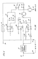
loop 10 receives a frequency error signal from thefrequency comparator 12 throughterminal 42. - Referring to Fig. 1B,
frequency comparator 12 comprises aninterval counter 43, adecoder 44 and a delay anderror voltage generator 45.Interval counter 43 includes anedge detector 46 which receives the input EFM bit stream throughterminal 40 to generate a narrow pulse in response to the transition at each rising and falling edge of the incoming bit stream for enabling acounter 47 and latches 48 and 49.Counter 47 is arranged to count the clock pulse supplied from theoscillator 19 throughterminal 41 in response to an enable pulse fromedge detector 46 and is reset in response to the arrival of the next enable pulse. The output ofcounter 47 is a binary code representing the' number of clock pulses present in each successive pulse duration and pulse separation of the input bit stream. This binary code output is fed to latch 48 in response to the enable pulse. The count stored inlatch 48 is fed todecoder 44 on the one hand and transferred tosecond latch 49 on the other hand. Thus, the counts inlatches latches -
Decoder 44 comprises a pair ofdigital comparators gates gates Comparators latches gates gate 54 to generate a pulse 81 when the total value of counts stored inlatches gate 55 combines the output ofOR gate 53 and the first output ofcomparator 50 and ANDgate 56 combines the output ofOR gate 52 and the first output ofcomparator 51. ORgate 57 combines the outputs of ANDgates latches - Delay and
error voltage generator 45 comprises a retriggerable monostable multivibrator 58 responsive to pulse S1 from ANDgate 54 andvoltage dividing resistors monostable multivibrators OR gate 57 to respond to pulse S2, and ANDgate 63, a retriggerable monostable multivibrator 64 andvoltage dividing resistors Resistors monostable multivibrators 58 and 64. - Retriggerable
monostable multivibrator 58 generates a pulse having a duration Tr longer than the frame period (=588 clock pulses) in response to the occurrence of a pulse Si. If the clock frequency is equal to or higher than normal, the pulse Si is generated at periodic frame intervals, causing the monostable 58 to generate an output pulse Pr shown at Fig. 3. As long as the VCO frequency is maintained at normal frequency, the output ofmonostable 58 is at high voltage level andresistors terminal 42. If the clock frequency drops below normal, pulse S1 no longer exists. Should this condition last for a period longer than the period Tr of monostable 58, the output of this monostable is reduced to a low level until the clock frequency is restored to normal, providing a negative-going, frequency error voltage pulse Fe1 to terminal 42 (Fig. 3). - On the other hand, pulse S2 drives monostable 61 to cause it to generate a pulse Sm1 with a duration smaller than the frame period as shown at Fig. 4. Pulse Sm1 in turn drives monostable 62 to generate a second pulse Sm2 with a duration smaller than the frame period. The total period of pulses Smi and Sm2 is greater than a frame period but smaller than two frame periods, so that pulse S2 on a second occurrence will coincide with a pulse Sm2. AND
gate 63 is enabled in response to the pulse Sm2 to pass a pulse S2 as an output Sm to retriggerable multivibrator 64 in the event that the clock frequency remains higher than normal for a period greater than a frame period. Retriggerable monostable multivibrator 64 is triggered in response to the pulse Sm on a first occurrence to generate a positive-going, frequency control voltage pulse Fe2. This retriggerable monostable multivibrator has a period slightly greater than a frame period. Therefore, if the clock frequency is still higher than normal, pulse Sm of a second occurrence will be generated to cause the multivibrator 64 to be retriggered. - From the foregoing, it will be seen that when the clock frequency is normal the total number of counts in
latches monostable multivibrator 58 is high and the output of monostable multivibrator 64 is low.Resistors noise suppressor 17 to the inverting input ofoperational amplifier 30. This medium voltage represents a neutral point at which theoscillator 19 is controlled to establish a phase-locked condition.Noise suppressor 17 includes a pair of antiparallel-connecteddiodes - When the clock frequency drops below normal, the total number of counts in the
latches Retriggerable multivibrator 58 remains high for period Tr after the cessation of pulse Si, whereupon it switches to a low output state. Since retriggerable multivibrator 64 has also been at low output state, the frequency control voltage Fe becomes lower than the neutral level. The inverting input ofoperational amplifier 30 is biased in a direction tending to cause theoscillator 19 to raise its output frequency. This low voltage bias is present continuously until the occurrence of a pulse S, when the oscillator frequency restores to normal. - Conversely, when the clock frequency rises above normal, the total number of counts in
latches retriggerable multivibrator 58 to switch to a high voltage as in the normal state. If the pulses 52 occur in succession, retriggerable multivibrator 64 is triggered in response to the second of the pulses S2 to generate a high output voltage. The high voltages at the outputs ofmultivibrators 58 and 64 are summed up to raise the potential at terminal 42 to a level higher than the neutral level. The inverting input ofoperational amplifier 30 is biased in a direction tending to cause theoscillator 19 to lower its output frequency. Retriggerable multivibrator 64 will be retriggered in response to a pulse S2 at third occurrence if the clock frequency is still higher than normal. When clock frequency returns to normal, the pulse S2 is no longer present and retriggerable multivibrator 64 is allowed to switch to a low voltage state one frame period after the occurrence of the third pulse S2, causing the error voltage Fe at terminal 42 to decrease to the neutral value. The high voltage bias is thus present continuously until the disappearance of pulse S2 when the oscillator frequency restores to normal. - Retriggerable monostable multivibrator 64 can be replaced with a flip-
flop 71, shown at Fig. 1C. This flip-flop has a set input connected to the output of ANDgate 63 and reset input connected to the output of ANDgate 54 to receive pulses Sm and S, respectively. As illustrated in Fig. 5, the operation of thefrequency comparator 12 with flip-flop 71 is similar to that just described with the exception that flip-flop 71 is triggered into a set condition in response to pulse Sm preferentially to the application of pulse S, to its reset terminal. Upon the disappearance of pulses S2, the flip-flop 71 is triggered into a reset condition in response to a pulse S1 that occurs immediately after the clock frequency returns to normal. The frequency error voltage Fe is thus sharply terminated in response to the next frame sync immediately after the disappearance of pulses S2. - Since the frequency comparator of the inven- . tion utilizes the periodicity of frame sync in the input EFM bit stream, the frequency error pulses S, and S2 occur quickly in response to the phase-locked loop going beyond its capture range and in sufficient numbers during the out-of-phase condition. Phase-locked condition can therefore be readily reestablished. As a result, the clock generator of the invention has a wider capture range than conventional clock generators in which the occurrences of data bits having predetermined periodic intervals are detected to derive frequency error control voltages.
- The delayed responses provided by retriggerable monostable multivibrator 58 and
monostable multivibrators - Fig. 6 is an illustration of an alternative embodiment of the phase-locked loop which is generally shown at
numeral 100 and in which parts corresponding to those in Fig. 1A are marked with the same numerals as used in Fig. 1A. The phase-lockedloop 100 differs from the phase-lockedloop 10 in that D flip-flops inverters OR gates NAND gate 21 of Fig. 1A. The output ofwindow pulse generator 13 is applied to the clear input of flip-flop 80 and throughinverter 83 to the clock input of flip-flop 81. Whereas, the output of voltage-controlledoscillator 19 is connected to the clock input of flip-flop 80 whose data input is impressed with a logical high voltage and throughinverter 82 to the data and clear terminals of flip-flop 81. The true Q output offlip-flop 80 and the Õ output of flip-flop 81 are connected to the resistor network formed byresistors 24 to 27. Flip-flop 84 has its data, clock and clear input terminals coupled together to the logical low voltage source and its true Q and complementary Q outputs connected toresistors 35 to 38. - The operation of the phase-locked
loop 100 is as follows. When clock pulses Pc are phase-locked with window pulses Pw as shown at Fig. 7A, the voltages at the outputs of flip-flops flop 80 produces a positive-goingpulse 80a (Fig. 7B) having a leading edge coincident with the leading edge of a clock pulse and a trailing edge coincident with the trailing edge of the window pulse, while the output of flip-flop 81 remains high. The positive-goingpulse 80a is combined with the high voltage at the output of flip-flop 81 to cause the potential at junction A to rise to a level higher than medium level M during the period ofpulse 80a to cause theoscillator 19 to lag the phase of the clock pulse in proportion to the amount of phase advance. If the clock pulse lags with respect to the window pulse, flip-flop 80 remains at low voltage state while flip-flop 81 generates a negative-going pulse 81a, as shown at Fig. 7C. This pulse has a leading edge coincident with the trailing edge of window pulse Pw and a trailing edge coincident with the leading edge of clock pulse Pc. The potential at junction A is reduced to a level lower than the medium level during the period of the pulse 81a to cause theoscillator 19 to advance the clock phase in proportion to the amount of phase lag. - The embodiments described above are particularly useful for adaptation to integrated circuits.
Claims (4)
Applications Claiming Priority (2)
| Application Number | Priority Date | Filing Date | Title |
|---|---|---|---|
| JP59057580A JPS60200635A (en) | 1984-03-26 | 1984-03-26 | Bit clock signal generating device of digital signal demodulating equipment |
| JP57580/84 | 1984-03-26 |
Publications (2)
| Publication Number | Publication Date |
|---|---|
| EP0158219A1 EP0158219A1 (en) | 1985-10-16 |
| EP0158219B1 true EP0158219B1 (en) | 1989-09-27 |
Family
ID=13059785
Family Applications (1)
| Application Number | Title | Priority Date | Filing Date |
|---|---|---|---|
| EP85103614A Expired EP0158219B1 (en) | 1984-03-26 | 1985-03-26 | Sync responsive clock generator for digital demodulators |
Country Status (4)
| Country | Link |
|---|---|
| US (1) | US4617526A (en) |
| EP (1) | EP0158219B1 (en) |
| JP (1) | JPS60200635A (en) |
| DE (1) | DE3573343D1 (en) |
Families Citing this family (13)
| Publication number | Priority date | Publication date | Assignee | Title |
|---|---|---|---|---|
| US4672329A (en) * | 1984-03-30 | 1987-06-09 | Victor Company Of Japan, Ltd. | Clock generator for digital demodulators |
| CA1284361C (en) * | 1986-08-29 | 1991-05-21 | Mitel Corporation | Analog phase locked loop |
| JPS6387835A (en) * | 1986-10-01 | 1988-04-19 | Victor Co Of Japan Ltd | Bit clock signal generator for digital signal demodulator |
| US4754216A (en) * | 1987-09-03 | 1988-06-28 | National Semiconductor Corporation | Method and apparatus for qualifying the decode window margin of a phase locked loop data synchronizer |
| JPH01269280A (en) * | 1988-04-20 | 1989-10-26 | Sony Corp | Optical disk device |
| EP0549154A3 (en) * | 1991-12-24 | 1993-12-08 | Advanced Micro Devices Inc | Repetitive pattern detection |
| DE69218374T2 (en) * | 1991-12-24 | 1997-10-02 | Advanced Micro Devices Inc | Detection of sector markings for optical data disks |
| JP3331711B2 (en) * | 1993-11-24 | 2002-10-07 | ソニー株式会社 | Clock signal generator |
| US5598396A (en) * | 1995-02-15 | 1997-01-28 | Matsushita Electric Industrial Co., Ltd. | Optical disk reproducing apparatus |
| DE19614979C2 (en) | 1995-04-20 | 2001-05-17 | Fujitsu Ltd | Radio frequency transceiver for data communication |
| US5946279A (en) * | 1996-04-30 | 1999-08-31 | Mitsumi Electric Co., Ltd. | Servo circuit, digital PLL circuit and optical disk device |
| JP2000341119A (en) | 1999-05-31 | 2000-12-08 | Nec Corp | Clock oscillation circuit |
| US6573759B2 (en) * | 2001-01-18 | 2003-06-03 | Nvision, Inc. | Apparatus and method for extracting data values from a signal encoded with AES3 data |
Citations (1)
| Publication number | Priority date | Publication date | Assignee | Title |
|---|---|---|---|---|
| EP0074793A1 (en) * | 1981-09-08 | 1983-03-23 | Fujitsu Limited | Phase-locked loop circuit |
Family Cites Families (6)
| Publication number | Priority date | Publication date | Assignee | Title |
|---|---|---|---|---|
| US3982194A (en) * | 1975-02-18 | 1976-09-21 | Digital Equipment Corporation | Phase lock loop with delay circuits for relative digital decoding over a range of frequencies |
| US4003086A (en) * | 1975-04-28 | 1977-01-11 | Memorex Corporation | Dynamic loop gain alteration for data retrieval |
| US4023116A (en) * | 1976-07-08 | 1977-05-10 | Fairchild Camera And Instrument Corporation | Phase-locked loop frequency synthesizer |
| US4131920A (en) * | 1977-10-19 | 1978-12-26 | Pioneer Magnetics | Closed-clock writing system for a rotating magnetic memory |
| US4191976A (en) * | 1978-09-26 | 1980-03-04 | Data General Corporation | Circuit indicating phase relationship |
| DE2906200C3 (en) * | 1979-02-17 | 1982-02-11 | Philips Patentverwaltung Gmbh, 2000 Hamburg | Synchronizing arrangement |
-
1984
- 1984-03-26 JP JP59057580A patent/JPS60200635A/en active Pending
-
1985
- 1985-03-25 US US06/715,246 patent/US4617526A/en not_active Expired - Fee Related
- 1985-03-26 EP EP85103614A patent/EP0158219B1/en not_active Expired
- 1985-03-26 DE DE8585103614T patent/DE3573343D1/en not_active Expired
Patent Citations (1)
| Publication number | Priority date | Publication date | Assignee | Title |
|---|---|---|---|---|
| EP0074793A1 (en) * | 1981-09-08 | 1983-03-23 | Fujitsu Limited | Phase-locked loop circuit |
Also Published As
| Publication number | Publication date |
|---|---|
| US4617526A (en) | 1986-10-14 |
| EP0158219A1 (en) | 1985-10-16 |
| JPS60200635A (en) | 1985-10-11 |
| DE3573343D1 (en) | 1989-11-02 |
Similar Documents
| Publication | Publication Date | Title |
|---|---|---|
| CA1070395A (en) | Versatile phase-locked loop phase detector | |
| US4085288A (en) | Phase locked loop decoder | |
| EP0158219B1 (en) | Sync responsive clock generator for digital demodulators | |
| US4596981A (en) | Synchronizing signal detecting circuit in a digital signal transmitting system | |
| EP0057612B1 (en) | Motor controlling circuit of reproducing apparatus and method of controlling | |
| CA1129990A (en) | Circuit indicating phase relationship | |
| US3602828A (en) | Self-clocking detection system | |
| US4346411A (en) | Amplitude sensitive three-level detector for derivative read back channel of magnetic storage device | |
| US4535306A (en) | Phase-locked loop detecting circuit | |
| US4472686A (en) | Circuit for reproducing and demodulating modulated digital signals | |
| US3840892A (en) | Method and device for detecting signals from magnetic memory | |
| JPS5891514A (en) | Signal conversion circuit | |
| US4628282A (en) | Clock generator for digital demodulators | |
| US4672329A (en) | Clock generator for digital demodulators | |
| US3938184A (en) | Digital flutter reduction system | |
| US4599736A (en) | Wide band constant duty cycle pulse train processing circuit | |
| US3879752A (en) | Combined sector pulse and data detection system | |
| US3656149A (en) | Three frequency data separator | |
| US4580100A (en) | Phase locked loop clock recovery circuit for data reproducing apparatus | |
| US3727143A (en) | Integrating level sensing circuit | |
| EP0023783A1 (en) | Data recovery circuit | |
| US4912573A (en) | Digital data reproducing apparatus having recording modulation mode detection | |
| US3493962A (en) | Converter for self-clocking digital signals | |
| JP2675096B2 (en) | Playback signal correction method | |
| JPH0879059A (en) | Reference clock generating circuit |
Legal Events
| Date | Code | Title | Description |
|---|---|---|---|
| PUAI | Public reference made under article 153(3) epc to a published international application that has entered the european phase |
Free format text: ORIGINAL CODE: 0009012 |
|
| AK | Designated contracting states |
Designated state(s): DE GB NL |
|
| 17P | Request for examination filed |
Effective date: 19860314 |
|
| 17Q | First examination report despatched |
Effective date: 19870817 |
|
| GRAA | (expected) grant |
Free format text: ORIGINAL CODE: 0009210 |
|
| AK | Designated contracting states |
Kind code of ref document: B1 Designated state(s): DE GB NL |
|
| REF | Corresponds to: |
Ref document number: 3573343 Country of ref document: DE Date of ref document: 19891102 |
|
| PLBE | No opposition filed within time limit |
Free format text: ORIGINAL CODE: 0009261 |
|
| STAA | Information on the status of an ep patent application or granted ep patent |
Free format text: STATUS: NO OPPOSITION FILED WITHIN TIME LIMIT |
|
| 26N | No opposition filed | ||
| PGFP | Annual fee paid to national office [announced via postgrant information from national office to epo] |
Ref country code: GB Payment date: 19940316 Year of fee payment: 10 |
|
| PGFP | Annual fee paid to national office [announced via postgrant information from national office to epo] |
Ref country code: DE Payment date: 19940323 Year of fee payment: 10 |
|
| PGFP | Annual fee paid to national office [announced via postgrant information from national office to epo] |
Ref country code: NL Payment date: 19940331 Year of fee payment: 10 |
|
| PG25 | Lapsed in a contracting state [announced via postgrant information from national office to epo] |
Ref country code: GB Effective date: 19950326 |
|
| PG25 | Lapsed in a contracting state [announced via postgrant information from national office to epo] |
Ref country code: NL Effective date: 19951001 |
|
| GBPC | Gb: european patent ceased through non-payment of renewal fee |
Effective date: 19950326 |
|
| NLV4 | Nl: lapsed or anulled due to non-payment of the annual fee |
Effective date: 19951001 |
|
| PG25 | Lapsed in a contracting state [announced via postgrant information from national office to epo] |
Ref country code: DE Effective date: 19951201 |