EP0156162A2 - Programmable controller - Google Patents
Programmable controller Download PDFInfo
- Publication number
- EP0156162A2 EP0156162A2 EP85101838A EP85101838A EP0156162A2 EP 0156162 A2 EP0156162 A2 EP 0156162A2 EP 85101838 A EP85101838 A EP 85101838A EP 85101838 A EP85101838 A EP 85101838A EP 0156162 A2 EP0156162 A2 EP 0156162A2
- Authority
- EP
- European Patent Office
- Prior art keywords
- memory
- sequence
- instruction
- instructions
- address
- Prior art date
- Legal status (The legal status is an assumption and is not a legal conclusion. Google has not performed a legal analysis and makes no representation as to the accuracy of the status listed.)
- Granted
Links
Images


Classifications
-
- G—PHYSICS
- G06—COMPUTING; CALCULATING OR COUNTING
- G06F—ELECTRIC DIGITAL DATA PROCESSING
- G06F9/00—Arrangements for program control, e.g. control units
- G06F9/06—Arrangements for program control, e.g. control units using stored programs, i.e. using an internal store of processing equipment to receive or retain programs
- G06F9/30—Arrangements for executing machine instructions, e.g. instruction decode
- G06F9/32—Address formation of the next instruction, e.g. by incrementing the instruction counter
- G06F9/322—Address formation of the next instruction, e.g. by incrementing the instruction counter for non-sequential address
-
- G—PHYSICS
- G05—CONTROLLING; REGULATING
- G05B—CONTROL OR REGULATING SYSTEMS IN GENERAL; FUNCTIONAL ELEMENTS OF SUCH SYSTEMS; MONITORING OR TESTING ARRANGEMENTS FOR SUCH SYSTEMS OR ELEMENTS
- G05B19/00—Programme-control systems
- G05B19/02—Programme-control systems electric
- G05B19/04—Programme control other than numerical control, i.e. in sequence controllers or logic controllers
- G05B19/05—Programmable logic controllers, e.g. simulating logic interconnections of signals according to ladder diagrams or function charts
-
- G—PHYSICS
- G06—COMPUTING; CALCULATING OR COUNTING
- G06F—ELECTRIC DIGITAL DATA PROCESSING
- G06F9/00—Arrangements for program control, e.g. control units
- G06F9/06—Arrangements for program control, e.g. control units using stored programs, i.e. using an internal store of processing equipment to receive or retain programs
- G06F9/30—Arrangements for executing machine instructions, e.g. instruction decode
- G06F9/30145—Instruction analysis, e.g. decoding, instruction word fields
-
- G—PHYSICS
- G05—CONTROLLING; REGULATING
- G05B—CONTROL OR REGULATING SYSTEMS IN GENERAL; FUNCTIONAL ELEMENTS OF SUCH SYSTEMS; MONITORING OR TESTING ARRANGEMENTS FOR SUCH SYSTEMS OR ELEMENTS
- G05B2219/00—Program-control systems
- G05B2219/10—Plc systems
- G05B2219/13—Plc programming
- G05B2219/13083—Jumps
Definitions
- the present invention relates to a programmable controller and more particularly to a programmable sequence controller.
- the programmable controller is a unit which processes input information by a processing unit (CPU) in accordance with a sequence program stored in a memory (RAM) by a user and selectively operates equipments connected to output terminals in accordance with the operation result to attain a programmed sequence control.
- the programming may be constructed by a sequencer language which is easy to use for the user, such as LOAD, AND and OR.
- a processing system for executing the sequencer language program by the processing unit includes an interpreter system in which a quasi-coded program is executed while it is sequentially decoded, and a compiler system in which the program is translated to a machine language so that it is instantly executed.
- the prior art programmable controller used one of those systems.
- the former system however, has drawbacks of long time required for decoding instructions and low processing speed, and in the latter system allows the processing unit (CPU) may overrun if the translated program is destroyed by an external disturbance such as noise because there is no check means.
- CPU processing unit
- a first memory unit for storing therein a sequence program including a combination of sequence instructions
- a second memory unit for storing therein machine language instructions corresponding to the sequence instructions at addresses designated by operation codes of the sequence instructions and a jump instruction with non-designated jump-to address
- a processing unit for executing sequence control in accordance with the instructions read from the second memory unit
- instruction transfer means for decoding a predetermined address signal supplied from the processing unit to read out a jump-to address following to the readout of the jump instruction, fetching the sequence instruction to be executed next from the first memory unit and transferring the operation code of that sequence instruction to the processing unit as the jump-to address.
- Numeral 1 denotes contacts which are input signal sources
- numeral 2 denotes an input unit which receives input signals from the contacts 1
- numeral 3 denotes a processing unit (CPU) for executing a sequence control
- numeral 4 denotes a readable and writable memory (user RAM) which is a first memory unit for storing therein a sequence program prepared by a user
- numeral 5 denotes a read-only memory (system ROM, a non-volatile memory) which is a second memory unit for storing therein a control procedure (system program) for executing the sequence program
- numeral 6 denotes an output unit for transferring the operation result of the CPU 3 to external equipments, not shown
- numeral 7 denotes a program unit for writing the sequence program keyed in by the user into the user RAM 4.
- Fig. 2 shows a circuit diagram of one embodiment of the present invention, -which-comprises-the CPU 3, the user RAM 4, the system ROM 5 and a peripheral circuit for transferring the operation code of the sequence instruction stored in the user RAM 4 and transferring a data in accordance with the sequence instruction.
- Numeral 8 denotes a data memory which is a readable and writable memory (RAM) for temporarily storing therein signals supplied to the input unit 2 of Fig. 1, signals to be supplied to the output unit 6 and the operation result of the CPU 3.
- Numeral 9 denotes an address bus
- numeral 13 denotes a first data bus which serves as a main transfer line of instructions and data
- numeral 14 denotes a second data bus which is used to write the sequence program into the user RAM 4.
- The_circuit for transferring the operation code and data includes the following elements.
- Numerals 15 and 16 denote address decoders. When an address signal from the CPU 3 is applied thereto, only the selected one of Y 1 , Y 2 and Y 3 assumes "0" and non-selected ones assume “I”.
- Numeral 17 denotes an OR gate
- numeral 18 denotes a NAND gate
- numeral 19 denotes an AND gate
- numeral 20 denotes an inverter. Those elements logically operate in accordance with the outputs of the address decoders 15 and 16.
- Numeral 21 denotes a step counter for selecting the contents of the user RAM 4 stepwise
- numeral 22 denotes a latch for latching the signal from the user RAM 4 at a predetermined timing
- numeral 23 denotes a buffer which receives the output of the latch 22 and transfers it to the CPU 3 through the data bus 13 at a predetermined timing.
- the buffer 23 has three output states "0", "1" and "High Impedance". Except when the signal from the user RAM 4 is transferred, the output state is "High Impedance" so that other data transfer on the first data bus 13 is not impeded.
- Numeral 24 denotes a selector which selects the signal from the user R A M 4 and the buffer 23 or the signal from the address bus 9 and supply the selected signal to the data memory 8
- numeral 25 an inverter which inverts or non-inverts the output of the data memory 8 and supplies it to the first data bus 13.
- Fig. 5 shows a portion of the system program stored in the system ROM 5.
- Machine language instructions corresponding to the instructions are stored at addresses ;shown by JMP, LOAD, AND, OR and OUT.
- a jump-to address of the JM2 (jump) instruction at address $7000 consists of two words, "70" and "XX". "XX" means that it is any code and the jump-to address is not designated.
- the "XX" portion of the non-designated jump-to address is determined by the operation code of the sequence instruction stored in the user RAM 4, and the machine language instructions corresponding to the sequence instructions such as LOAD, AND, OR, OUT are stored at addresses designated by the operation codes of the sequence instructions, that is, jump-to addresses of the JMP instruction ($7000) designated by the operation codes.
- the JMP instructions at the addresses 7012, 7022, 7032 and 7042 are used to return the program to the address $7000 when the processing is executed in accordance with the sequence instructions.
- the addresses $7080 et seq contain an error check and error processing program which is used when the content of the user RAM 4 is destroyed. This will be explained later.
- the CPU 3 supplies a predetermined address signal (for example, $7000) to the address bus 9, the output Y3 of the address decoder 15 is selected and the output "0" thereof is supplied to the OR gate 17 and the address decoder 16 so that the decoder 16 is enabled.
- a predetermined address signal for example, $7000
- the output Y 1 of the address decoder 16 is selected and the output "0" thereof is produced. Since the non-selected output Y 3 of the decoder 16 is “1”, the output of the inverter 20 is “0" and the OR gate 17 produces the “0” output.
- the system ROM 5 is selected by the output of the OR gate 17 and the content at the address $7000 shown in Fig: 5 is read out. Since the output Y 1 of the address decoder 16 is "0" and the output Y 2 is "1", the NAND gate 18 produces "1" output on the stepping line 26 of the step counter 21. Thus, the step counter 21 is incremented by one and the signal thereof is transferred to the user RAM 4. Thus, the user RAM 4 is selected stepwise and the H-byte of the sequence instruction shown in Fig. 3 (the operation code, the inversion code and a portion of the I/O number) is read out.
- the CPU 3 supplies the address signal stored at $7001 to the address bus 9 to read out the next content of the system ROM 5, that is, the content at $7001.
- the latch 22 is enabled by the trailing edge of'the output Y l of the address decoder 16 to latch the H-byte of the sequence instruction read from the user RAM 4. The timing therefor is shown in Fig. 7.
- the output Y 3 of the address decoder 15 is selected and the output Y 2 of the address decoder 16 is selected. Accordingly, the output of the OR gate 17 is "0" and the system ROM 5 remains selected. Since the output Y 1 of the address decoder 16 is "1" and the output Y 2 is "0", the NAND gate 18 again produces the "1" output on the stepping line 26 so that the step counter 21 is incremented by one. Accordingly, the L-byte of the sequence instruction shown in Fig. 3 (remaining portion of the I/O number) is read out.
- the CPU 3 supplies the address signal stored at $7002 to the address bus 9 to read out the content at the address $7002.
- the Y - output of the address decoder 15 is selected and the output Y 3 of the address decoder 16 is selected and the "0" output thereof is inverted by the inverter 20.
- the output of the OR gate 17 is "1" and the system ROM 5 is non-selected and the buffer 23 is selected by the output Y 3 of the address decoder 16.
- the buffer 23 receives the content latched in the latch 22, that is, five bits of the operation code in the H-byte of the sequence instruction stored in the user RAM 4 and constructs an 8-bit code by adding "0" to three low order bits, and supplies the 8-bit code to the data bus 13. Accordingly, the CPU 3 fetches the 8-bit instruction code through the buffer 23 instead of the content at the address $7002 of the system ROM 5.
- the timing therefor is shown in Fig. 7.
- the output Y 3 of the address decoder 15 is "0" and the output Y 3 of the address decoder 16 is "1” and the system ROM 5 is selected again. Accordingly, the processing by the CPU 3 is jumped to the jump-to address $7010.
- the CPU 3 Since the address $7010 contains the LOAD instruction instructing to "read address $40", the CPU 3 supplies the signal $40 to the address bus 9. Thus, the output Y 2 of the address decoder 15 assumes “0” and the output "0" is supplied to the AND gate 19 through the select line 27 and the data memory 8 is selected by the output "0" of the AND gate 19. The address decoder 15 is organized to let the output Y 2 "0" based on the signal $40.
- the inverter 25 inverts or non-inverts the signal from the data memory 8 depending on whether the inversion code bit of the sequence instruction latched in the latch 22 is "1" or "0". It is used to invert the input signal from the contact b.
- CPU 3 then read out the content at the address $7012 and executes it. Since the address $7012 contains "JMP 7000", that is, "jump to the address $7000", the processing of the CPU 3 again jumps to the address $7000.
- the execution of the sequence instruction shown in Fig. 3 is thus terminated and the next sequence instruction (logical AND of the input signal at the contact 11) is started.
- the machine language instruction corresponding to the sequence instruction is selected by the JMP instruction at the address $7000. Only the jump-to-address "XX" is different.
- the jump-to address is determined by the operation code stored in the user RAM 4 and the CPU 3 executes the machine language instruction at the designated jump-to address.
- the processing speed is significantly improved.
- the processing speed was 40 ms/kw in the interpreter system while it is 20 ms/kw or less in the present system.
- the instructions for the operand codes are stored in the system ROM 5 as the machine language instruction, the instructions are not destroyed by an external disturbance such as a noise and the safety is guaranteed.
- the error check and error processing routine may be stored in the system ROM 5 as a part of the system program, the safety is assumed even if the content of the user RAM 4 is destroyed by the external disturbance such as noise.
- several undefined operation codes 80, 90 - F0,00
- JMP 7800 is stored at each of the addresses corresponding to the undefined operand codes as shown in Fig. 5.
- the function of the selector 24 is now explained.
- the signals from the user RAM 4 and the latch 22 are supplied to the address line 29 through the selector 24.
- the output Y 1 of the address decoder 15 is selected and the output signal thereof is supplied to the selector 24 through the select line 28.
- the selector 24 selects the signal such that the signal on the address bus 9 is supplied to the address line 29.
- the CPU 3 is allowed to directly access the data memory 8 as required.
- the CPU 3 can read in the signals of the contacts 1 in Fig. 1 and store them in the data memory 8 and transfer the specified content of the data memory 8 to the output unit 6 by the direct access between the CPU 3 and the data memory 8 without intervention of the user RAM 4. Accordingly, high speed data processing is attained.
- the signals of the contacts 1 are collectively read at each scan time and stored in the data memory 8, and the specified content of the data memory 8 is read out by the signal from the user R AM 4.
- the I/O number read from the user RAM 4 may be latched and it is supplied to the CPU 3 through the buffer at a predetermined timing in the same manner as that of the reading of the specified content of the data memory 8 by the signal from the user RAM 4 so that the input signal from the specific contact is read in without routing the memory each time the instruction is executed. The same is time for the data output to the output unit 6.
- the machine language instruction corresponding to the sequence instruction is selected using the operation code of the sequence instruction as the jump-to address. Accordingly, it is not necessary to interprete the operation code each time it is fetched as is done in the prior art interpreter system and the processing speed is increased. Since the machine language instructions and the error processing routine are stored in the memory such as system ROM the content of which will not be destroyed by the external disturbance, the overrun of the CPU which occurred in the prior art compiler system is prevented and the safety is enhanced.
Abstract
Description
- The present invention relates to a programmable controller and more particularly to a programmable sequence controller.
- The programmable controller is a unit which processes input information by a processing unit (CPU) in accordance with a sequence program stored in a memory (RAM) by a user and selectively operates equipments connected to output terminals in accordance with the operation result to attain a programmed sequence control. The programming may be constructed by a sequencer language which is easy to use for the user, such as LOAD, AND and OR.
- A processing system for executing the sequencer language program by the processing unit (CPU) includes an interpreter system in which a quasi-coded program is executed while it is sequentially decoded, and a compiler system in which the program is translated to a machine language so that it is instantly executed. The prior art programmable controller used one of those systems.
- The former system, however, has drawbacks of long time required for decoding instructions and low processing speed, and in the latter system allows the processing unit (CPU) may overrun if the translated program is destroyed by an external disturbance such as noise because there is no check means.
- Since those problems directly relate to the performance and safety of the programmable controller, solutions thereof have been desired.
- It is an object of the present invention to provide a programmable controller having a high processing speed.
- It is another object of the present invention to provide a sequence controller in which a processing unit hardly overruns.
- In accordance with the present invention, there are provided a first memory unit for storing therein a sequence program including a combination of sequence instructions, a second memory unit for storing therein machine language instructions corresponding to the sequence instructions at addresses designated by operation codes of the sequence instructions and a jump instruction with non-designated jump-to address, a processing unit for executing sequence control in accordance with the instructions read from the second memory unit, and instruction transfer means for decoding a predetermined address signal supplied from the processing unit to read out a jump-to address following to the readout of the jump instruction, fetching the sequence instruction to be executed next from the first memory unit and transferring the operation code of that sequence instruction to the processing unit as the jump-to address.
-
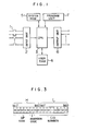
- Fig. 1 is a block diagram of a basic configuration of a programmable controller;
- Fig. 2 is a circuit diagram of one embodiment of the present invention;
- Fig. 3 shows an example of a sequence program stored in a user RAM of Fig. 2;
- Fig. 4 is a table of an instruction word and an operation code;
- Fig. 5 is an example of a system program stored in an system ROM of Fig. 2,
- Fig. 6 is a sequence chart for illustrating an operation; and
- Fig. 7 is a timing chart therefor.
- A basic configuration of the programmable controller is shown in Fig. 1. Numeral 1 denotes contacts which are input signal sources,
numeral 2 denotes an input unit which receives input signals from the contacts 1,numeral 3 denotes a processing unit (CPU) for executing a sequence control,numeral 4 denotes a readable and writable memory (user RAM) which is a first memory unit for storing therein a sequence program prepared by a user,numeral 5 denotes a read-only memory (system ROM, a non-volatile memory) which is a second memory unit for storing therein a control procedure (system program) for executing the sequence program,numeral 6 denotes an output unit for transferring the operation result of theCPU 3 to external equipments, not shown, andnumeral 7 denotes a program unit for writing the sequence program keyed in by the user into theuser RAM 4. - Fig. 2 shows a circuit diagram of one embodiment of the present invention, -which-comprises-the
CPU 3, theuser RAM 4, thesystem ROM 5 and a peripheral circuit for transferring the operation code of the sequence instruction stored in theuser RAM 4 and transferring a data in accordance with the sequence instruction. Numeral 8 denotes a data memory which is a readable and writable memory (RAM) for temporarily storing therein signals supplied to theinput unit 2 of Fig. 1, signals to be supplied to theoutput unit 6 and the operation result of theCPU 3. Numeral 9 denotes an address bus, numeral 13 denotes a first data bus which serves as a main transfer line of instructions and data, and numeral 14 denotes a second data bus which is used to write the sequence program into theuser RAM 4. - The_circuit for transferring the operation code and data includes the following elements.
-
Numerals CPU 3 is applied thereto, only the selected one of Y1, Y2 and Y3 assumes "0" and non-selected ones assume "I". Numeral 17 denotes an OR gate,numeral 18 denotes a NAND gate, numeral 19 denotes an AND gate, andnumeral 20 denotes an inverter. Those elements logically operate in accordance with the outputs of theaddress decoders user RAM 4 stepwise,numeral 22 denotes a latch for latching the signal from theuser RAM 4 at a predetermined timing, andnumeral 23 denotes a buffer which receives the output of thelatch 22 and transfers it to theCPU 3 through the data bus 13 at a predetermined timing. Thebuffer 23 has three output states "0", "1" and "High Impedance". Except when the signal from theuser RAM 4 is transferred, the output state is "High Impedance" so that other data transfer on the first data bus 13 is not impeded. Numeral 24 denotes a selector which selects the signal from the user RAM 4 and thebuffer 23 or the signal from the address bus 9 and supply the selected signal to the data memory 8, and numeral 25 an inverter which inverts or non-inverts the output of the data memory 8 and supplies it to the first data bus 13. - Fig. 3 shows an example of the sequence program stored in the
user RAM 4. One sequence instruction comprises 16 bits of which 5 bits are used for an operation code, 1 bit is used for an inversion code and 10 bits are used for an I/O number. Since theuser RAM 4 uses a general- purpose 8-bit memory, each sequence instruction is divided into an 8-bit H byte and an 8-bit L byte, which are sequentially stored in this order. The sequence program comprises a plurality of such sequence instructions. The operation code may be expressed in any manner. For example, it has one-to-one correspondence to the sequencer language instructions (LOAD, AND, OR, OUT, etc.) as shown in Fig. 4. - In Fig. 3, low order three bits of the operation code are omitted. "00010" shown therein corresponds to "00010000" in the 8-bit code (or $10 in a hexadicimal expression).
- Undefined operation codes in Fig. 4 are provided for use in error checking, which will be explained later.
- Fig. 5 shows a portion of the system program stored in the
system ROM 5. Machine language instructions corresponding to the instructions are stored at addresses ;shown by JMP, LOAD, AND, OR and OUT. A jump-to address of the JM2 (jump) instruction at address $7000 consists of two words, "70" and "XX". "XX" means that it is any code and the jump-to address is not designated. The "XX" portion of the non-designated jump-to address is determined by the operation code of the sequence instruction stored in theuser RAM 4, and the machine language instructions corresponding to the sequence instructions such as LOAD, AND, OR, OUT are stored at addresses designated by the operation codes of the sequence instructions, that is, jump-to addresses of the JMP instruction ($7000) designated by the operation codes. The JMP instructions at the addresses 7012, 7022, 7032 and 7042 are used to return the program to the address $7000 when the processing is executed in accordance with the sequence instructions. The addresses $7080 et seq contain an error check and error processing program which is used when the content of theuser RAM 4 is destroyed. This will be explained later. - The operation of the present invention is explained for a sequence shown in Fig. 6.
- When the
CPU 3 supplies a predetermined address signal (for example, $7000) to the address bus 9, the output Y3 of theaddress decoder 15 is selected and the output "0" thereof is supplied to the OR gate 17 and theaddress decoder 16 so that thedecoder 16 is enabled. - The output Y1 of the
address decoder 16 is selected and the output "0" thereof is produced. Since the non-selected output Y3 of thedecoder 16 is "1", the output of theinverter 20 is "0" and the OR gate 17 produces the "0" output. Thesystem ROM 5 is selected by the output of the OR gate 17 and the content at the address $7000 shown in Fig: 5 is read out. Since the output Y1 of theaddress decoder 16 is "0" and the output Y2 is "1", theNAND gate 18 produces "1" output on thestepping line 26 of thestep counter 21. Thus, thestep counter 21 is incremented by one and the signal thereof is transferred to theuser RAM 4. Thus, theuser RAM 4 is selected stepwise and the H-byte of the sequence instruction shown in Fig. 3 (the operation code, the inversion code and a portion of the I/O number) is read out. - Since the content at the address $7000 is the JMP instruction, the
CPU 3 supplies the address signal stored at $7001 to the address bus 9 to read out the next content of thesystem ROM 5, that is, the content at $7001. Thelatch 22 is enabled by the trailing edge of'the output Yl of theaddress decoder 16 to latch the H-byte of the sequence instruction read from theuser RAM 4. The timing therefor is shown in Fig. 7. - As the address signal at $7001 is generated, the output Y3 of the
address decoder 15 is selected and the output Y2 of theaddress decoder 16 is selected. Accordingly, the output of the OR gate 17 is "0" and thesystem ROM 5 remains selected. Since the output Y1 of theaddress decoder 16 is "1" and the output Y2 is "0", theNAND gate 18 again produces the "1" output on thestepping line 26 so that thestep counter 21 is incremented by one. Accordingly, the L-byte of the sequence instruction shown in Fig. 3 (remaining portion of the I/O number) is read out. - Then, the
CPU 3 supplies the address signal stored at $7002 to the address bus 9 to read out the content at the address $7002. The Y- output of theaddress decoder 15 is selected and the output Y3 of theaddress decoder 16 is selected and the "0" output thereof is inverted by theinverter 20. Thus, the output of the OR gate 17 is "1" and thesystem ROM 5 is non-selected and thebuffer 23 is selected by the output Y3 of theaddress decoder 16. Thebuffer 23 receives the content latched in thelatch 22, that is, five bits of the operation code in the H-byte of the sequence instruction stored in theuser RAM 4 and constructs an 8-bit code by adding "0" to three low order bits, and supplies the 8-bit code to the data bus 13. Accordingly, theCPU 3 fetches the 8-bit instruction code through thebuffer 23 instead of the content at the address $7002 of thesystem ROM 5. The timing therefor is shown in Fig. 7. - The CPU has thus fetched "70" and "XX=10" from the addresses $7001 and $7002 of the
system ROM 5. It then supplies the address signal $7010 to the address bus 9. Thus, the output Y3 of theaddress decoder 15 is "0" and the output Y3 of theaddress decoder 16 is "1" and thesystem ROM 5 is selected again. Accordingly, the processing by theCPU 3 is jumped to the jump-to address $7010. - Since the address $7010 contains the LOAD instruction instructing to "read address $40", the
CPU 3 supplies the signal $40 to the address bus 9. Thus, the output Y2 of theaddress decoder 15 assumes "0" and the output "0" is supplied to the AND gate 19 through theselect line 27 and the data memory 8 is selected by the output "0" of the AND gate 19. Theaddress decoder 15 is organized to let the output Y2 "0" based on the signal $40. Since the I/O number in the L-byte of the sequence instruction fetched from theuser RAM 4 and the I/O number in the H-byte of the sequence instruction latched in thelatch 22 are supplied to theaddress line 29 of the data memory 8 through theselector 24, the contents of the data memory corresponding to the above I/O numbers are supplied to the data bus 13 through the inverter 25 and supplied to theCPU 3. Since the current sequence instruction is "Read input signal ofcontact 10", the input signal from the contact 10 (Hexadecimal) which has previously been stored in the data memory 8 is fetched by theCPU 3. - The inverter 25 inverts or non-inverts the signal from the data memory 8 depending on whether the inversion code bit of the sequence instruction latched in the
latch 22 is "1" or "0". It is used to invert the input signal from the contact b. -
CPU 3 then read out the content at the address $7012 and executes it. Since the address $7012 contains "JMP 7000", that is, "jump to the address $7000", the processing of theCPU 3 again jumps to the address $7000. - The execution of the sequence instruction shown in Fig. 3 is thus terminated and the next sequence instruction (logical AND of the input signal at the contact 11) is started. In the following execution of the instruction, the machine language instruction corresponding to the sequence instruction is selected by the JMP instruction at the address $7000. Only the jump-to-address "XX" is different. The jump-to address is determined by the operation code stored in the
user RAM 4 and theCPU 3 executes the machine language instruction at the designated jump-to address. - Since the operation code of the sequence instruction stored in the
user RAM 4 is read by theCPU 3 as the jump-to address and machine language instruction stored in thesystem ROM 5 is addressed in accordance with the sequence instruction, the instruction decode routine which was necessary in the prior art interpreter system can be omitted and the fetched instruction can be instantly executed. Accordingly, the processing speed is significantly improved. For example, the processing speed was 40 ms/kw in the interpreter system while it is 20 ms/kw or less in the present system. - Since the instructions for the operand codes are stored in the
system ROM 5 as the machine language instruction, the instructions are not destroyed by an external disturbance such as a noise and the safety is guaranteed. In the present system, since the error check and error processing routine may be stored in thesystem ROM 5 as a part of the system program, the safety is assumed even if the content of theuser RAM 4 is destroyed by the external disturbance such as noise. For example, in case the content of theuser RAM 4 is destroyed, several undefined operation codes (80, 90 - F0,00) are provided as shown in Fig. 4 and "JMP 7800" is stored at each of the addresses corresponding to the undefined operand codes as shown in Fig. 5. Assuming that the address $7800 contains the error processing routine, the overrun of theCPU 3 is avoided and an alarm may be issued even if the content of theuser RAM 4 is destroyed, by the jump to the error processing routine from the jump-to address corresponding to the undefined operation code. - The function of the
selector 24 is now explained. The signals from theuser RAM 4 and thelatch 22 are supplied to theaddress line 29 through theselector 24. When theCPU 3 generates a specific address signal, the output Y1 of theaddress decoder 15 is selected and the output signal thereof is supplied to theselector 24 through theselect line 28. Thus, theselector 24 selects the signal such that the signal on the address bus 9 is supplied to theaddress line 29. Thus, theCPU 3 is allowed to directly access the data memory 8 as required. Through this function, theCPU 3 can read in the signals of the contacts 1 in Fig. 1 and store them in the data memory 8 and transfer the specified content of the data memory 8 to theoutput unit 6 by the direct access between theCPU 3 and the data memory 8 without intervention of theuser RAM 4. Accordingly, high speed data processing is attained. - In the above embodiment, the signals of the contacts 1 are collectively read at each scan time and stored in the data memory 8, and the specified content of the data memory 8 is read out by the signal from the user RAM 4. Alternatively, the I/O number read from the
user RAM 4 may be latched and it is supplied to theCPU 3 through the buffer at a predetermined timing in the same manner as that of the reading of the specified content of the data memory 8 by the signal from theuser RAM 4 so that the input signal from the specific contact is read in without routing the memory each time the instruction is executed. The same is time for the data output to theoutput unit 6. - In accordance with the present invention, the machine language instruction corresponding to the sequence instruction is selected using the operation code of the sequence instruction as the jump-to address. Accordingly, it is not necessary to interprete the operation code each time it is fetched as is done in the prior art interpreter system and the processing speed is increased. Since the machine language instructions and the error processing routine are stored in the memory such as system ROM the content of which will not be destroyed by the external disturbance, the overrun of the CPU which occurred in the prior art compiler system is prevented and the safety is enhanced.
Claims (12)
Applications Claiming Priority (2)
| Application Number | Priority Date | Filing Date | Title |
|---|---|---|---|
| JP59058056A JPH0830971B2 (en) | 1984-03-26 | 1984-03-26 | Programmable controller |
| JP58056/84 | 1984-03-26 |
Publications (3)
| Publication Number | Publication Date |
|---|---|
| EP0156162A2 true EP0156162A2 (en) | 1985-10-02 |
| EP0156162A3 EP0156162A3 (en) | 1987-10-28 |
| EP0156162B1 EP0156162B1 (en) | 1991-07-10 |
Family
ID=13073252
Family Applications (1)
| Application Number | Title | Priority Date | Filing Date |
|---|---|---|---|
| EP85101838A Expired EP0156162B1 (en) | 1984-03-26 | 1985-02-20 | Programmable controller |
Country Status (4)
| Country | Link |
|---|---|
| US (1) | US4879678A (en) |
| EP (1) | EP0156162B1 (en) |
| JP (1) | JPH0830971B2 (en) |
| DE (1) | DE3583405D1 (en) |
Cited By (2)
| Publication number | Priority date | Publication date | Assignee | Title |
|---|---|---|---|---|
| EP0446359A1 (en) * | 1989-09-27 | 1991-09-18 | Fanuc Ltd. | Method of data loading in numeric controller |
| EP0555513A2 (en) * | 1992-02-13 | 1993-08-18 | Koyo Electronics Industries Co., Ltd. | Control method in programmable controller |
Families Citing this family (4)
| Publication number | Priority date | Publication date | Assignee | Title |
|---|---|---|---|---|
| JP2978189B2 (en) * | 1989-11-16 | 1999-11-15 | シャープ株式会社 | Automatic flowchart creation device |
| US5379388A (en) * | 1992-07-08 | 1995-01-03 | Advanced Micro Devices, Inc. | Digital signal processing apparatus with sequencer designating program routines |
| JP3738134B2 (en) * | 1998-06-19 | 2006-01-25 | 三洋電機株式会社 | Digital signal processor |
| US8832670B2 (en) * | 2011-07-01 | 2014-09-09 | Mitsubishi Electric Corporation | Programmable controller and programming tool for communication with legacy equipment |
Citations (2)
| Publication number | Priority date | Publication date | Assignee | Title |
|---|---|---|---|---|
| US4302820A (en) * | 1979-08-20 | 1981-11-24 | Allen-Bradley Company | Dual language programmable controller |
| FR2508193A1 (en) * | 1981-06-19 | 1982-12-24 | Toyoda Machine Works Ltd | PROGRAMMABLE SEQUENCE CONTROL DEVICE |
Family Cites Families (12)
| Publication number | Priority date | Publication date | Assignee | Title |
|---|---|---|---|---|
| US3518413A (en) * | 1968-03-21 | 1970-06-30 | Honeywell Inc | Apparatus for checking the sequencing of a data processing system |
| US4058850A (en) * | 1974-08-12 | 1977-11-15 | Xerox Corporation | Programmable controller |
| US4205370A (en) * | 1975-04-16 | 1980-05-27 | Honeywell Information Systems Inc. | Trace method and apparatus for use in a data processing system |
| US4307445A (en) * | 1978-11-17 | 1981-12-22 | Motorola, Inc. | Microprogrammed control apparatus having a two-level control store for data processor |
| US4231089A (en) * | 1978-12-15 | 1980-10-28 | Digital Equipment Corporation | Data processing system with apparatus for correcting microinstruction errors |
| US4484303A (en) * | 1979-06-19 | 1984-11-20 | Gould Inc. | Programmable controller |
| US4336602A (en) * | 1979-09-24 | 1982-06-22 | Control Data Corporation | Network for generating modified microcode addresses |
| US4370729A (en) * | 1980-03-21 | 1983-01-25 | Point 4 Data Corporation | Microprogram sequencer |
| JPS5769413A (en) * | 1980-10-16 | 1982-04-28 | Omron Tateisi Electronics Co | Programmable logic controller |
| US4432052A (en) * | 1981-04-13 | 1984-02-14 | Texas Instruments Incorporated | Microcomputer device using dispatch addressing of control ROM |
| US4439828A (en) * | 1981-07-27 | 1984-03-27 | International Business Machines Corp. | Instruction substitution mechanism in an instruction handling unit of a data processing system |
| US4573118A (en) * | 1983-03-31 | 1986-02-25 | Fairchild Camera & Instrument Corporation | Microprocessor with branch control |
-
1984
- 1984-03-26 JP JP59058056A patent/JPH0830971B2/en not_active Expired - Lifetime
-
1985
- 1985-02-15 US US06/702,264 patent/US4879678A/en not_active Expired - Fee Related
- 1985-02-20 DE DE8585101838T patent/DE3583405D1/en not_active Expired - Lifetime
- 1985-02-20 EP EP85101838A patent/EP0156162B1/en not_active Expired
Patent Citations (2)
| Publication number | Priority date | Publication date | Assignee | Title |
|---|---|---|---|---|
| US4302820A (en) * | 1979-08-20 | 1981-11-24 | Allen-Bradley Company | Dual language programmable controller |
| FR2508193A1 (en) * | 1981-06-19 | 1982-12-24 | Toyoda Machine Works Ltd | PROGRAMMABLE SEQUENCE CONTROL DEVICE |
Cited By (4)
| Publication number | Priority date | Publication date | Assignee | Title |
|---|---|---|---|---|
| EP0446359A1 (en) * | 1989-09-27 | 1991-09-18 | Fanuc Ltd. | Method of data loading in numeric controller |
| EP0446359A4 (en) * | 1989-09-27 | 1992-10-21 | Fanuc Ltd. | Method of data loading in numeric controller |
| EP0555513A2 (en) * | 1992-02-13 | 1993-08-18 | Koyo Electronics Industries Co., Ltd. | Control method in programmable controller |
| EP0555513A3 (en) * | 1992-02-13 | 1994-01-19 | Koyo Electronics Ind Co |
Also Published As
| Publication number | Publication date |
|---|---|
| EP0156162B1 (en) | 1991-07-10 |
| JPH0830971B2 (en) | 1996-03-27 |
| EP0156162A3 (en) | 1987-10-28 |
| DE3583405D1 (en) | 1991-08-14 |
| JPS60201402A (en) | 1985-10-11 |
| US4879678A (en) | 1989-11-07 |
Similar Documents
| Publication | Publication Date | Title |
|---|---|---|
| US3983541A (en) | Polymorphic programmable units employing plural levels of phased sub-instruction sets | |
| US6272596B1 (en) | Data processor | |
| US10872642B2 (en) | System comprising a memory capable of implementing calculation operations | |
| US4446517A (en) | Microprogram memory with page addressing and address decode in memory | |
| US4251862A (en) | Control store organization in a microprogrammed data processing system | |
| US4821183A (en) | A microsequencer circuit with plural microprogrom instruction counters | |
| US4306285A (en) | Data processing apparatus | |
| JPH0332818B2 (en) | ||
| EP0156162A2 (en) | Programmable controller | |
| EP0229734A2 (en) | Microprogram control device | |
| EP0395377B1 (en) | Status register for microprocessor | |
| EP0358773B1 (en) | Microcomputer | |
| US4635188A (en) | Means for fast instruction decoding for a computer | |
| US4831572A (en) | Polynomial vector arithmetic operation control system | |
| KR950009687B1 (en) | High speed ladder instruction processing apparatus for programnable logic controller | |
| US5155826A (en) | Memory paging method and apparatus | |
| KR19980086928A (en) | Internal and External Memory Usage | |
| US4675843A (en) | Programmable logic controller | |
| US4089051A (en) | Alternative direct and indirect addressing | |
| US5619714A (en) | Microcomputer having an instruction decoder with a fixed area and a rewritable area | |
| EP0503498A2 (en) | Single-chip microcomputer with program/data memory flag | |
| KR100230184B1 (en) | Memory table look-up device and method | |
| US6507884B1 (en) | Microcomputer with multiple memories for storing data | |
| KR940000221B1 (en) | Ladder command processor apparatus | |
| JP2720401B2 (en) | Instruction memory range expansion device |
Legal Events
| Date | Code | Title | Description |
|---|---|---|---|
| PUAI | Public reference made under article 153(3) epc to a published international application that has entered the european phase |
Free format text: ORIGINAL CODE: 0009012 |
|
| AK | Designated contracting states |
Designated state(s): DE GB IT NL |
|
| PUAL | Search report despatched |
Free format text: ORIGINAL CODE: 0009013 |
|
| AK | Designated contracting states |
Kind code of ref document: A3 Designated state(s): DE GB IT NL |
|
| 17P | Request for examination filed |
Effective date: 19871030 |
|
| 17Q | First examination report despatched |
Effective date: 19890704 |
|
| GRAA | (expected) grant |
Free format text: ORIGINAL CODE: 0009210 |
|
| AK | Designated contracting states |
Kind code of ref document: B1 Designated state(s): DE GB IT NL |
|
| REF | Corresponds to: |
Ref document number: 3583405 Country of ref document: DE Date of ref document: 19910814 |
|
| ITF | It: translation for a ep patent filed |
Owner name: MODIANO & ASSOCIATI S.R.L. |
|
| PLBE | No opposition filed within time limit |
Free format text: ORIGINAL CODE: 0009261 |
|
| STAA | Information on the status of an ep patent application or granted ep patent |
Free format text: STATUS: NO OPPOSITION FILED WITHIN TIME LIMIT |
|
| 26N | No opposition filed | ||
| PGFP | Annual fee paid to national office [announced via postgrant information from national office to epo] |
Ref country code: GB Payment date: 19970210 Year of fee payment: 13 |
|
| PG25 | Lapsed in a contracting state [announced via postgrant information from national office to epo] |
Ref country code: GB Free format text: LAPSE BECAUSE OF NON-PAYMENT OF DUE FEES Effective date: 19980220 |
|
| GBPC | Gb: european patent ceased through non-payment of renewal fee |
Effective date: 19980220 |
|
| PGFP | Annual fee paid to national office [announced via postgrant information from national office to epo] |
Ref country code: NL Payment date: 19990228 Year of fee payment: 15 |
|
| PG25 | Lapsed in a contracting state [announced via postgrant information from national office to epo] |
Ref country code: NL Free format text: LAPSE BECAUSE OF NON-PAYMENT OF DUE FEES Effective date: 20000901 |
|
| NLV4 | Nl: lapsed or anulled due to non-payment of the annual fee |
Effective date: 20000901 |
|
| PGFP | Annual fee paid to national office [announced via postgrant information from national office to epo] |
Ref country code: DE Payment date: 20040304 Year of fee payment: 20 |