EP0146229B1 - Apparatus for expanding illuminated picture elements in crt displays - Google Patents
Apparatus for expanding illuminated picture elements in crt displays Download PDFInfo
- Publication number
- EP0146229B1 EP0146229B1 EP84307140A EP84307140A EP0146229B1 EP 0146229 B1 EP0146229 B1 EP 0146229B1 EP 84307140 A EP84307140 A EP 84307140A EP 84307140 A EP84307140 A EP 84307140A EP 0146229 B1 EP0146229 B1 EP 0146229B1
- Authority
- EP
- European Patent Office
- Prior art keywords
- picture elements
- illuminated
- delay
- picture element
- shift register
- Prior art date
- Legal status (The legal status is an assumption and is not a legal conclusion. Google has not performed a legal analysis and makes no representation as to the accuracy of the status listed.)
- Expired - Lifetime
Links
Images


Classifications
-
- G—PHYSICS
- G09—EDUCATION; CRYPTOGRAPHY; DISPLAY; ADVERTISING; SEALS
- G09G—ARRANGEMENTS OR CIRCUITS FOR CONTROL OF INDICATING DEVICES USING STATIC MEANS TO PRESENT VARIABLE INFORMATION
- G09G1/00—Control arrangements or circuits, of interest only in connection with cathode-ray tube indicators; General aspects or details, e.g. selection emphasis on particular characters, dashed line or dotted line generation; Preprocessing of data
- G09G1/002—Intensity circuits
-
- G—PHYSICS
- G09—EDUCATION; CRYPTOGRAPHY; DISPLAY; ADVERTISING; SEALS
- G09G—ARRANGEMENTS OR CIRCUITS FOR CONTROL OF INDICATING DEVICES USING STATIC MEANS TO PRESENT VARIABLE INFORMATION
- G09G1/00—Control arrangements or circuits, of interest only in connection with cathode-ray tube indicators; General aspects or details, e.g. selection emphasis on particular characters, dashed line or dotted line generation; Preprocessing of data
- G09G1/06—Control arrangements or circuits, of interest only in connection with cathode-ray tube indicators; General aspects or details, e.g. selection emphasis on particular characters, dashed line or dotted line generation; Preprocessing of data using single beam tubes, e.g. three-dimensional or perspective representation, rotation or translation of display pattern, hidden lines, shadows
- G09G1/14—Control arrangements or circuits, of interest only in connection with cathode-ray tube indicators; General aspects or details, e.g. selection emphasis on particular characters, dashed line or dotted line generation; Preprocessing of data using single beam tubes, e.g. three-dimensional or perspective representation, rotation or translation of display pattern, hidden lines, shadows the beam tracing a pattern independent of the information to be displayed, this latter determining the parts of the pattern rendered respectively visible and invisible
- G09G1/146—Flicker reduction circuits
Definitions
- the present invention relates generally to CRT displays, and more particularly to the expansion of illuminated picture elements therein in order to increase writing speed and eliminate flicker resulting from line pair destruction by higher priority symbols.
- Lines written on a CRT display comprise discrete picture elements. Each picture element is either illuminated or not. A line is written, picture element by picture element, from left to right.
- the entire set of lines written on a CRT display denoted a frame, comprises two fields. The first field comprises the odd numbered lines which are written from the top to the bottom of the CRT display. The second field comprises the even numbered lines which are also written, after the entire first field has been written, from the top to the bottom of the CRT display. Each of the two fields may be written in one-sixtieth of a second, providing a frame in one-thirtieth of a second.
- the picture information written on the CRT display is read from an image memory.
- the image memory comprises a number of addresses, each of which contains a "1" or a "0" bit.
- a "1" read from an address in the image memory produces illumination of the corresponding picture element in the CRT display.
- a "0" read from an address in the image memory engenders no illumination of the corresponding picture element in the CRT display.
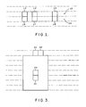
- a line 12 written in one-sixtieth of a second on a CRT display comprises illuminated picture elements 13, 14 and 15.
- a viewer perceives the illuminated picture elements 13, 14 and 15 to flicker.
- the phenomenon is remedied by duplicating the illuminated picture elements 13, 14, and 15 with, respectively, illuminated picture elements 16, 17, and 18 on an adjacent line 19.
- a lower priority symbol 20 comprises illuminated picture elements 21 and 22 on a line 23 in one field, and illuminated picture elements 24 and 25 on an adjacent line 26 in the other field. As indicated above, the illuminated picture elements 24 and 25 duplicate, respectively, the illuminated picture elements 21 and 22 to prevent flickering.
- a higher priority symbol 28 comprises an illuminated picture element 29 on a line 30 in one field, and a duplicate illuminated picture element 31 on an adjacent line 32, in the other field.
- a mask 34 extends three lines above, and surrounds the higher priority symbol 28. Referring now to Figure 3, the higher priority symbol 28 may move upwards such that the mask 34 erases the duplicate illuminated picture elements 24 and 25. With the elimination of the duplicate illuminated picture elements 24 and 25, the remaining illuminated picture elements 21 and 22 flicker.
- the address reading means comprises a first shift register, having two compartments, for loading in parallel with video bit signals from addresses corresponding to picture elements P I,J and P I-1,J ; and comprises a second shift register, having two compartments, for loading in parallel with video bit signals from addresses corresponding to picture elements P I,J+1 and P I-1,J+1 .
- a first delay preferably comprising a shift register, is coupled to the first shift register.
- a second delay preferably comprising a D type flip-flop, is coupled to the first delay; and a third delay, preferably comprising a D type flip-flop, is coupled to the second shift register.
- the present invention increases writing speed and eliminates disconcerting flickering.
- the present invention is concerned with apparatus for expanding illuminated picture elements in a CRT display wherein lines are written relatively slowly. Such expansion increases writing speed and prevents flickering resulting from the erasure of interlaced illuminated picture elements by the mask of a higher priority symbol.
- An image memory contains a number of addresses which are designated by x and y coordinates. The coordinates are in binary notation.
- video bit signals for a video character are written in addresses in the image memory such that the picture elements on a CRT display corresponding to these addresses are separated on a given line by one picture elements, and occupy lines which are separated by one picture element. This is achieved by writing video bit signals into only addresses whose x coordinate possesses a fixed first binary digit, and whose y coordinate possesses a fixed first binary digit.
- the corresponding addresses utilised in the image memory may be chosen to possess an x coordinate whose first digit is 0, and to possess a y coordinate whose first digit is 1.
- Any video character may possess any x , y combination of 1 and 0.
- the memory comprises an eight by eight matrix of addresses, the x coordinate available to a given character of the addresses varies from 000 to 111, and the y coordinate available to a given character varies from 000 to 111.
- Video bit signals for the given character may be written into only these addresses in the image memory.
- the invention entails writing picture information into such selected addresses in the image memory, and expanding the written information so that no gaps appear on the CRT.
- an illuminated picture element must be duplicated below on the next line of the CRT display.
- picture information is written into the addresses in the image memory in the alternating fashion described above, a duplicate illuminated picture element would appear on the CRT display one line below the original illuminated picture element.
- each illuminated picture element on the CRT display is duplicated on the vacant line immediately therebelow.
- each illuminated picture element always possesses at least one flicker-eliminating duplicate.
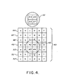
- a higher priority symbol 40 comprising a "written into memory” and illuminated picture element 41 and duplicate illuminated picture elements 42, 43 and 44, is surrounded by a black mask 45.
- the black mask 45 comprises picture elements 46a through 46f on a line 46, picture elements 47a through 47f on a line 47, picture elements 48a through 48f on a line 48, picture elements 49a through 49d on a line 49, picture elements 50a through 50d on a line 50, picture elements 51a through 51f on a line 51, and picture elements 52a through 52e on a line 52.
- a lower priority symbol 53 comprises written into memory and illuminated picture element 54 and its respective duplicates 55, 56 and 57 generated by the invention.
- Symbols on the CRT display comprising picture elements corresponding to the selected addresses in the image memory, can occupy any of the interlacing lines comprising the picture. Accordingly, vertical movement of symbols entails one line at a time but is not restricted to such.
- the illuminated picture element 54 is further expanded into adjacent illuminated picture elements 55 and 57.
- Such horizontal expansions do not affect flickering, but serve to double the speed of picture generation.
- Vertical expansions using pels 56 and 57 serve to avoid flicker and to double the writing speed for a net speed increase of 2 horizontally by 2 vertically equals 4 overall.
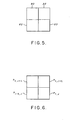
- each illuminated picture element 80 is expanded below in an illuminated picture element 81, and to double writing speed, the illuminated picture element 80 is expanded to the right in an illuminated picture element 82, and expanded below and to the right in an illuminated picture element 83.
- each picture element as the CRT display beam scans from left to right and from top to bottom. Denoting the current picture element with which the CRT beam generator is aligned as P I,J , the adjacent picture elements P I-1 J, P I-1,J+1' and P I,J+1 are considered.
- This situation corresponds to a "1" being in the image memory addressed location of the currently aligned picture element P 1'J. Accordingly, P I,J is illuminated by the CRT beam. If the CRT beam generator is currently aligned with the picture element 82, then the picture element 82 is desired to be illuminated since it is an expansion of the illuminated picture element 80 to its left. This situation corresponds to a "1" being in the image memory address of the picture element P I,J which is to the left of the currently aligned picture element P I,J . Accordingly, P I,J is illuminated. If the CRT beam generator is currently aligned with the picture element 81, then the picture element 81 is desired to be illuminated since it is an expansion of the illuminated picture element 80 above it.
- This situation corresponds to a "1" being in the image memory address of the picture element P I,J+1 which is above the currently aligned picture element P I,J .
- P I,J is illuminated accordingly. If the CRT beam gnerator is currently aligned with the picture element 83, then the picture element 83 is desired to be illuminated since it is an expansion of the illuminated picture element 80 which is above and to the left of it. This situation corresponds to a "1" being in the image memory address of the picture element PI-1,J+1 which is above and to the left of the currently aligned picture element P I,J . P I,J is illuminated accordingly.
- the currently aligned picture element P I,J is illuminated when the Boolean "OR" sum of the video bit signals in the image memory addresses of the picture elements P I,J ; P I-1, J ; P I-1,J+1 and P I,J+1 is 1.
- the Boolean "OR” sum is zero the picture element P I,J , is unilluminated.
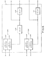
- a coordinator 90 coupled to a CRT display 91, generates, coordinates and aligns the beam generator of the CRT display with picture elements corresponding to the generated coordinates.
- the coordinator 90 is also coupled to an address reader 92 which in turn is coupled to an image memory 93.
- the address reader 92 in response to a signal from the coordinator 90 representing the coordinate of the picture element with which the beam generator is currently aligned, reads from the image memory 93 the video bit signals in the four addresses associated with the currently aligned picture element.
- the video bit signals B I,J ; B I-1,J ; B I-1,J+1 ; and B I,J+1 in the addresses of the image memory 93 corresponding, respectively, to the picture elements P I,J ; P I-1,J ; P I-1,J+1 ; and P I,J+1 are read from the image memory 93 by the address reader 92.
- These four video bit signals are conveyed by the address reader 92 to an OR gate 94.
- the OR gate 94 generates the Boolean OR sum:- of the four video bit signals.
- a digital-to-analogue converter 95 receives the digital sum signal from the OR gate 94 and converts it to an analogue signal.
- the beam generator of the CRT display receives the analogue signal produced by the digital-to-analogue converter 95. In response to an analogue signal corresponding to a digitial signal of ONE, a beam is generated which illuminates the picture element P I,J . An analogue signal corresponding to a ZERO digital signal engenders no illumination of the picture element P I,J .
- the address reader 92 comprises shift registers and delays.
- a shift register 100 is loaded in parallel, with the video bit signal B I-1,J received by a compartment 101 and the video bit signal B I,J received by a compartment 102.
- a shift register 104 is then loaded in parallel, with the video bit signal B I-1,J+1 received by a compartment 105 and the video bit signal B I,J+1 received by a compartment 106.
- the shift register 100 serially outputs the contents of the compartments 101 and 102 and the shift register 104 serially outputs the contents of the compartments 105 and 106.
- the outputs of the shift register 100 are received by a delay 108 which synchronises the outputs of the shift register 100 with those of the shift register 104. That is, the first output of the delay 108, B I-1,J , coincides with the first output of the shift register 104, B I-1,J+1 ; and, the second output of the delay 108, B I,J , coincides with the second output of the shift register 104, B I,J+1 . Video bit signals having the same x coordinate are thereby outputed at the same time.
- the delay 108 preferably comprises a shift register.
- the first output of the delay 108, B I-1,J is conveyed to a delay 110.
- each of the delays 110 and 111 preferably comprises a standard D-type flip-flop. If desired, the address reader may be altered to accommodate more than two video bit signals from a row of addresses in the image memory.
- the number of compartments in the shift registers 100 and 104 are merely increased to receive the additional video bit signals.
- the shift register comprising the delay 108 is similarly expanded, and the delays 110 and 111 are each coupled in series with additional similar delays, each also preferably comprising a D-type flip-flop.
- the various components described in Figure 7 are well-known in the art or readily contrived by one of ordinary skill therein.
- the image memory 93, the OR gate 94, the digital-to-analogue converter 95, the CRT display 91 and the coordinator 90 are conventional, well-known apparatus.
- One of ordinary skill in the art could readily design alternative versions of the address reader 92 described above, which would be suitable for purposes of the present invention.
Landscapes
- Engineering & Computer Science (AREA)
- Radar, Positioning & Navigation (AREA)
- Remote Sensing (AREA)
- Physics & Mathematics (AREA)
- Computer Hardware Design (AREA)
- General Physics & Mathematics (AREA)
- Theoretical Computer Science (AREA)
- Controls And Circuits For Display Device (AREA)
- Image Generation (AREA)
Description
- The present invention relates generally to CRT displays, and more particularly to the expansion of illuminated picture elements therein in order to increase writing speed and eliminate flicker resulting from line pair destruction by higher priority symbols.
- Lines written on a CRT display comprise discrete picture elements. Each picture element is either illuminated or not. A line is written, picture element by picture element, from left to right. The entire set of lines written on a CRT display, denoted a frame, comprises two fields. The first field comprises the odd numbered lines which are written from the top to the bottom of the CRT display. The second field comprises the even numbered lines which are also written, after the entire first field has been written, from the top to the bottom of the CRT display. Each of the two fields may be written in one-sixtieth of a second, providing a frame in one-thirtieth of a second. The picture information written on the CRT display is read from an image memory. The image memory comprises a number of addresses, each of which contains a "1" or a "0" bit. A one-to-one correspondence exists between the' addresses in the image memory and the picture elements in the CRT display. A "1" read from an address in the image memory produces illumination of the corresponding picture element in the CRT display. A "0" read from an address in the image memory engenders no illumination of the corresponding picture element in the CRT display.
- When a field is written in a relatively slow time, such as one-thirtieth of a second, illuminated picture elements on a given line create a flicker which is disconcerting to a viewer. Flickering, it has been found, can be eliminated by duplicating the illuminated picture elements on an adjacent line. For example, referring to Figure 1 of the accompanying drawings, a
line 12 written in one-sixtieth of a second on a CRT display comprisesilluminated picture elements illuminated picture elements illuminated picture elements picture elements adjacent line 19. When theline 12 is written in one field and thereafter theadjacent replica line 19 is written in another field, the viewer does not experience flickering of thepicture elements - Moving symbols in CRT displays possess various priority levels. Such symbols are surrounded by a mask, an invisible rectangle, which erases symbols of lower priority. In this fashion, higher priority symbols are precluded from merging with lower priority ones. However, the obliteration of a portion of a lower priority symbol by a higher priority one can produce flickering, by destroying duplicated illuminated picture elements. Referring to Figure 2 of the accompanying drawings, a
lower priority symbol 20 comprisesilluminated picture elements line 23 in one field, and illuminatedpicture elements adjacent line 26 in the other field. As indicated above, theilluminated picture elements illuminated picture elements higher priority symbol 28 comprises anilluminated picture element 29 on aline 30 in one field, and a duplicateilluminated picture element 31 on anadjacent line 32, in the other field. Amask 34 extends three lines above, and surrounds thehigher priority symbol 28. Referring now to Figure 3, thehigher priority symbol 28 may move upwards such that themask 34 erases the duplicateilluminated picture elements illuminated picture elements illuminated picture elements - Thus, there is a need for apparatus, utilised with a CRT display wherein lines are written relatively slowly, for preventing disconcerting flickering on the display resulting from the erasure of duplicate illuminated picture elements by higher priority symbols.
- The present invention is defined in the appended claims and a preferred embodiment, the address reading means comprises a first shift register, having two compartments, for loading in parallel with video bit signals from addresses corresponding to picture elements PI,J and PI-1,J ; and comprises a second shift register, having two compartments, for loading in parallel with video bit signals from addresses corresponding to picture elements PI,J+1 and PI-1,J+1. A first delay, preferably comprising a shift register, is coupled to the first shift register. A second delay, preferably comprising a D type flip-flop, is coupled to the first delay; and a third delay, preferably comprising a D type flip-flop, is coupled to the second shift register.
- By expanding illuminated picture elements, the present invention increases writing speed and eliminates disconcerting flickering.
- The invention will now be described in greater detail, by way of example, with reference to the accompanying drawings, in which:-
- Figure 1 is a schematic diagram illustrating duplication of illuminated picture elements in CRT displays in order to eliminate flickering (as already discussed),
- Figure 2 is a schematic diagram of a higher priority symbol surrounded by a black mask, and a lower priority symbol in a CRT display (as already discussed),
- Figure 3 is a schematic diagram illustrating the obliteration of duplicate illuminated picture elements of the lower priority symbol by the black mask of the higher priority symbol (as already discussed),
- Figure 4 is a schematic diagram of a higher priority symbol surrounded by a black mask, and a lower priority symbol written on a CRT display in accordance with the present invention,
- Figure 5 is a schematic diagram illustrating expansion of an arbitrary illuminated picture element in accordance with the present invention,
- Figure 6 is a schematic diagram of the picture elements whose memory address contents determine the illumination status of the picture element PI,J,
- Figure 7 is a block diagram of a preferred embodiment of the present invention, and
- Figure 8 is a block diagram of an address reader utilised in the preferred embodiment of the present invention.
- Identical numerals in different figures of drawings represent similar elements.
- The present invention is concerned with apparatus for expanding illuminated picture elements in a CRT display wherein lines are written relatively slowly. Such expansion increases writing speed and prevents flickering resulting from the erasure of interlaced illuminated picture elements by the mask of a higher priority symbol.
- An image memory contains a number of addresses which are designated by x and y coordinates. The coordinates are in binary notation. In the present invention, video bit signals for a video character are written in addresses in the image memory such that the picture elements on a CRT display corresponding to these addresses are separated on a given line by one picture elements, and occupy lines which are separated by one picture element. This is achieved by writing video bit signals into only addresses whose x coordinate possesses a fixed first binary digit, and whose y coordinate possesses a fixed first binary digit. For example, to generate spaces between picture elements within a line, and spaces between lines on the CRT display, the corresponding addresses utilised in the image memory may be chosen to possess an x coordinate whose first digit is 0, and to possess a y coordinate whose first digit is 1. Any video character may possess any x, y combination of 1 and 0. Assuming that the memory comprises an eight by eight matrix of addresses, the x coordinate available to a given character of the addresses varies from 000 to 111, and the y coordinate available to a given character varies from 000 to 111. Choosing only those addresses having an x coordinate whose first binary digit is 0, and having y coordinate whose first binary digit is 1 results in addresses available to a given character:
(000,001)=(0,1)(010,001)=(2,1)(100,001)=(4,1)(110,001)=(6,1)
(000,011)=(0,3)(010,011)=(2,3)(100,011)=(4,3)(110,011)=(6,3)
(000,101)=(0,5)(010,101)=(2,5)(100,101)=(4,5)(110,101)=(6,5)
(000,111)=(0,7)(010,111)=(2,7)(100,111)=(4,7)(110,111)=(6,7)
In this fashion, every other address may be selected in a given row and every other row maybe selected. Video bit signals for the given character may be written into only these addresses in the image memory. By holding the first binary digit of both the x and y coordinates of the addresses fixed, such an alternating pattern of addresses may be generated. The invention entails writing picture information into such selected addresses in the image memory, and expanding the written information so that no gaps appear on the CRT. - As indicated in the description of the prior art, to prevent flickering, an illuminated picture element must be duplicated below on the next line of the CRT display. When picture information is written into the addresses in the image memory in the alternating fashion described above, a duplicate illuminated picture element would appear on the CRT display one line below the original illuminated picture element. To prevent flickering resulting from an erasure, by the mask of a higher priority symbol, each illuminated picture element on the CRT display is duplicated on the vacant line immediately therebelow.
- In this fashion, each illuminated picture element always possesses at least one flicker-eliminating duplicate. For example, referring to Figure 4, a
higher priority symbol 40, comprising a "written into memory" andilluminated picture element 41 and duplicateilluminated picture elements black mask 45. Theblack mask 45 comprises picture elements 46a through 46f on a line 46, picture elements 47a through 47f on aline 47, picture elements 48a through 48f on aline 48, picture elements 49a through 49d on aline 49, picture elements 50a through 50d on aline 50, picture elements 51a through 51f on aline 51, and picture elements 52a through 52e on aline 52. Alower priority symbol 53 comprises written into memory and illuminatedpicture element 54 and itsrespective duplicates - Symbols on the CRT display, comprising picture elements corresponding to the selected addresses in the image memory, can occupy any of the interlacing lines comprising the picture. Accordingly, vertical movement of symbols entails one line at a time but is not restricted to such.
- Thus, referring to Figure 5, if the
higher priority symbol 40 moves upward, its second motion results in the picture elements 46e and 46d of theblack mask 45 intersecting, respectively, the duplicateilluminated picture elements element 54, thepicture elements - This flickering is eliminated by the duplicate
illuminated picture elements - Referring again to Figure 4, the
illuminated picture element 54 is further expanded into adjacentilluminated picture elements expansions using pels - Accordingly, referring to Figure 5, to prevent flickering each
illuminated picture element 80 is expanded below in anilluminated picture element 81, and to double writing speed, theilluminated picture element 80 is expanded to the right in anilluminated picture element 82, and expanded below and to the right in anilluminated picture element 83. This is accomplished by considering each picture element as the CRT display beam scans from left to right and from top to bottom. Denoting the current picture element with which the CRT beam generator is aligned as PI,J, the adjacent picture elements PI-1 J, PI-1,J+1' and PI,J+1 are considered. Referring to Figure 6, if there is a video bit signal of 1 in one or more of the four addresses in the image memory corresponding to these four picture elements, then the picture element PI,J' with which the CRT beam generator is currently aligned, is illuminated by the beam. This procedure effects the expansion of each illuminated picture element in the desired fashion depicted in Figure 5. This follows since the procedure implements the illuminated picture element expansion from the perspective of the picture element with which the CRT beam generator is currently aligned. Referring to Figures 5 and 6, if the CRT beam generator is currently aligned with thepicture element 80 whose image memory addressed location contains a "1", then thepicture element 80 is desired to be illuminated. This situation corresponds to a "1" being in the image memory addressed location of the currently aligned picture element P1'J. Accordingly, PI,J is illuminated by the CRT beam. If the CRT beam generator is currently aligned with thepicture element 82, then thepicture element 82 is desired to be illuminated since it is an expansion of theilluminated picture element 80 to its left. This situation corresponds to a "1" being in the image memory address of the picture element PI,J which is to the left of the currently aligned picture element PI,J. Accordingly, PI,J is illuminated. If the CRT beam generator is currently aligned with thepicture element 81, then thepicture element 81 is desired to be illuminated since it is an expansion of theilluminated picture element 80 above it. This situation corresponds to a "1" being in the image memory address of the picture element PI,J+1 which is above the currently aligned picture element PI,J. PI,J is illuminated accordingly. If the CRT beam gnerator is currently aligned with thepicture element 83, then thepicture element 83 is desired to be illuminated since it is an expansion of theilluminated picture element 80 which is above and to the left of it. This situation corresponds to a "1" being in the image memory address of the picture element PI-1,J+1 which is above and to the left of the currently aligned picture element PI,J. PI,J is illuminated accordingly. - In this fashion, by illuminating the picture element PI,J , with which the CRT beam generator is currently aligned, when any of the image memory addresses of the picture elements PI,J ; PI-1,J ; PI-1,J+1 ; PI,J+1 contains a 1, an illuminated picture element is expanded below to the right, and below and to the right, as required to prevent flickering and increase writing speed.
- This expansion procedure can be described mathematically. The currently aligned picture element PI,J is illuminated when the Boolean "OR" sum of the video bit signals in the image memory addresses of the picture elements PI,J ; PI-1, J ; PI-1,J+1 and PI,J+1 is 1. When the Boolean "OR" sum is zero the picture element PI,J , is unilluminated. Denoting the illumination status of the currently aligned picture element PI,J by IS, gives:-

where BX,Y is the video bit signal in the image memory address of the picture element PX,Y. - Referring to Figure 7, the above expansion procedure can be implemented as follows. A
coordinator 90, coupled to aCRT display 91, generates, coordinates and aligns the beam generator of the CRT display with picture elements corresponding to the generated coordinates. Thecoordinator 90 is also coupled to anaddress reader 92 which in turn is coupled to animage memory 93. Theaddress reader 92, in response to a signal from thecoordinator 90 representing the coordinate of the picture element with which the beam generator is currently aligned, reads from theimage memory 93 the video bit signals in the four addresses associated with the currently aligned picture element. That is, denoting as before, the currently aligned picture element as PI,J ' the video bit signals BI,J ; BI-1,J ; BI-1,J+1 ; and BI,J+1 in the addresses of theimage memory 93 corresponding, respectively, to the picture elements PI,J ; PI-1,J ; PI-1,J+1 ; and PI,J+1 are read from theimage memory 93 by theaddress reader 92. These four video bit signals are conveyed by theaddress reader 92 to anOR gate 94. TheOR gate 94 generates the Boolean OR sum:-
of the four video bit signals. A digital-to-analogue converter 95 receives the digital sum signal from theOR gate 94 and converts it to an analogue signal. - The beam generator of the CRT display receives the analogue signal produced by the digital-to-
analogue converter 95. In response to an analogue signal corresponding to a digitial signal of ONE, a beam is generated which illuminates the picture element PI,J . An analogue signal corresponding to a ZERO digital signal engenders no illumination of the picture element PI,J. - Referring to Figure 8, in a preferred embodiment of the invention, the
address reader 92 comprises shift registers and delays. Ashift register 100 is loaded in parallel, with the video bit signal BI-1,J received by acompartment 101 and the video bit signal BI,J received by acompartment 102. After a delay, ashift register 104 is then loaded in parallel, with the video bit signal BI-1,J+1 received by acompartment 105 and the video bit signal BI,J+1 received by acompartment 106. Theshift register 100 serially outputs the contents of thecompartments shift register 104 serially outputs the contents of thecompartments shift register 100 are received by adelay 108 which synchronises the outputs of theshift register 100 with those of theshift register 104. That is, the first output of thedelay 108, BI-1,J , coincides with the first output of theshift register 104, BI-1,J+1 ; and, the second output of thedelay 108, BI,J , coincides with the second output of theshift register 104, BI,J+1 . Video bit signals having the same x coordinate are thereby outputed at the same time. Thedelay 108 preferably comprises a shift register. The first output of thedelay 108, BI-1,J, is conveyed to adelay 110. The outputing of BI-1,J , from thedelay 110 coincides with the outputing of BI,J from thedelay 108. Similarly, the first output of theshift register 104, BI-1,J+1 , is conveyed to adelay 111. The outputing of BI-1 , from thedelay 111 coincides with the outputing of BI,J+1 from theshift register 104. In this fashion, the 4 video bit signals are available for conveyance at the same time to theOR gate 94 of Figure 7. Each of thedelays delay 108 is similarly expanded, and thedelays image memory 93, theOR gate 94, the digital-to-analogue converter 95, theCRT display 91 and thecoordinator 90 are conventional, well-known apparatus. One of ordinary skill in the art could readily design alternative versions of theaddress reader 92 described above, which would be suitable for purposes of the present invention.
Claims (8)
- Apparatus for expanding illuminated picture elements in video display means, comprising:
Means (91) for displaying video data comprising a matrix of picture elements, denoted PX,Y , and means for illuminating the picture elements in response to applied signals; means (90), coupled to the video display means, for generating coordinates, for providing signals representative of the coordinates, and for synchronising the illuminating means with the coordinates; means (93) for storing video bit signals, comprising addresses corresponding to the picture elements, each of the addresses being identified by a x and a y binary coordinate, the video bit signals being stored only in the addresses whose x coordinate has a predetermined first binary digit, and whose y coordinate has a predetermined first binary digit; means (92), responsive to a signal from the coordinate generating means representing a generated coordinate I,J, for reading the addresses corresponding to picture elements PI,J , PI-1,J , PI-1,J+1 , PI,J+1 ; means (94) coupled to the address reading means, for generating a Boolean OR sum digital signal from the video bit signals read from the addresses corresponding to picture elements PI,J ; PI-1,J ; PI-1,J+1 ; and PI,J+1 ; and means (95) coupled to the Boolean OR sum digital signal generating means and said video displaying means for generating, in response to a ZERO digital signal, a first analogue signal, and for generating, in response to a ONE digital signal, a second analogue signal, the picture element PI,J being illuminated by the illuminating means of the video display means in response to the second analogue signal, and the picture element PI,J being unilluminated by the illuminating means in response to the first analogue signal. - Apparatus according to claim 1, characterised in that the storing means comprises an image memory (93).
- Apparatus according to claim 1 or 2, characterised in that the video display means comprises a CRT display (91).
- Apparatus according to any of the preceding claims, characterised in that the address reading means comprises a first shift register (100) comprising the compartments (101, 102); a second shift register (104) comprising two compartments (105, 106); a first delay (108) coupled to the first shift register (100) ; a second delay (110) coupled to the first delay; and a third delay (111) coupled to the second shift register.
- Apparatus according to claim 4, characterised in that the first delay comprises a shift register (108).
- Apparatus according to claim 4 or 5 characterised in that the second delay comprises a D-type flip-flop (110) and the third delay comprises a D type flip-flop (111).
- Apparatus according to any of the preceding claims, characterised in that the Boolean OR sum digital signal, generating means comprises a Boolean OR gate (94) having four input terminals.
- Apparatus according to any of the preceding claims, characterised in that the converting means comprises a digital-to-analogue converter (95).
Applications Claiming Priority (2)
| Application Number | Priority Date | Filing Date | Title |
|---|---|---|---|
| US553224 | 1983-11-18 | ||
| US06/553,224 US4649378A (en) | 1983-11-18 | 1983-11-18 | Binary character generator for interlaced CRT display |
Publications (3)
| Publication Number | Publication Date |
|---|---|
| EP0146229A2 EP0146229A2 (en) | 1985-06-26 |
| EP0146229A3 EP0146229A3 (en) | 1988-05-11 |
| EP0146229B1 true EP0146229B1 (en) | 1991-05-29 |
Family
ID=24208616
Family Applications (1)
| Application Number | Title | Priority Date | Filing Date |
|---|---|---|---|
| EP84307140A Expired - Lifetime EP0146229B1 (en) | 1983-11-18 | 1984-10-17 | Apparatus for expanding illuminated picture elements in crt displays |
Country Status (6)
| Country | Link |
|---|---|
| US (1) | US4649378A (en) |
| EP (1) | EP0146229B1 (en) |
| JP (1) | JPS60119599A (en) |
| DE (1) | DE3484648D1 (en) |
| DK (1) | DK164339C (en) |
| IL (1) | IL73401A (en) |
Families Citing this family (11)
| Publication number | Priority date | Publication date | Assignee | Title |
|---|---|---|---|---|
| JPS6219890A (en) * | 1985-07-19 | 1987-01-28 | 株式会社東芝 | Display controller |
| US5276778A (en) * | 1987-01-08 | 1994-01-04 | Ezel, Inc. | Image processing system |
| US5553170A (en) * | 1987-07-09 | 1996-09-03 | Ezel, Inc. | High speed image processing system having a preparation portion and a converting portion generating a processed image based on the preparation portion |
| US5283866A (en) * | 1987-07-09 | 1994-02-01 | Ezel, Inc. | Image processing system |
| US4952921A (en) * | 1988-06-09 | 1990-08-28 | Rockwell International Corporation | Graphic dot flare apparatus |
| GB2223918B (en) * | 1988-10-14 | 1993-05-19 | Sun Microsystems Inc | Method and apparatus for optimizing selected raster operations |
| US5510843A (en) * | 1994-09-30 | 1996-04-23 | Cirrus Logic, Inc. | Flicker reduction and size adjustment for video controller with interlaced video output |
| US5611041A (en) * | 1994-12-19 | 1997-03-11 | Cirrus Logic, Inc. | Memory bandwidth optimization |
| US5963262A (en) * | 1997-06-30 | 1999-10-05 | Cirrus Logic, Inc. | System and method for scaling images and reducing flicker in interlaced television images converted from non-interlaced computer graphics data |
| EP1579481B1 (en) * | 2002-06-26 | 2013-12-04 | Semequip, Inc. | A method of semiconductor manufacturing by the implantation of boron hydride cluster ions |
| US7502024B2 (en) * | 2003-09-25 | 2009-03-10 | Honeywell International Inc. | Texture based circular arc generation |
Family Cites Families (12)
| Publication number | Priority date | Publication date | Assignee | Title |
|---|---|---|---|---|
| US3789386A (en) * | 1972-06-30 | 1974-01-29 | Takachiho Koeki Kk | Restoration system for pattern information using and-type logic of adjacent bits |
| US3921164A (en) * | 1974-06-03 | 1975-11-18 | Sperry Rand Corp | Character generator for a high resolution dot matrix display |
| US4107662A (en) * | 1976-02-17 | 1978-08-15 | Hitachi, Ltd. | Character generator for visual display devices |
| JPS5945155B2 (en) * | 1976-07-09 | 1984-11-05 | 株式会社日立製作所 | display device |
| DE2640759C2 (en) * | 1976-09-10 | 1982-10-14 | Robert Bosch Gmbh, 7000 Stuttgart | System for reproducing video signals |
| US4119954A (en) * | 1977-03-15 | 1978-10-10 | Burroughs Corporation | High resolution character generator for digital display units |
| JPS5422725A (en) * | 1977-07-21 | 1979-02-20 | Nec Corp | Character generating method |
| JPS5556247A (en) * | 1978-10-20 | 1980-04-24 | Hitachi Ltd | Raster scanning graphic display unit |
| NL7901119A (en) * | 1979-02-13 | 1980-08-15 | Philips Nv | IMAGE DISPLAY FOR DISPLAYING A TWO-INTERLINE TELEVISION IMAGE OF A TWO-VALUE SIGNAL GENERATED BY AN IMAGE SIGNAL GENERATOR. |
| GB2044051B (en) * | 1979-03-09 | 1982-11-24 | Miller Rickard Ltd | Resistive interpolation of extra elements and lines between stored data |
| GB2096866B (en) * | 1981-04-10 | 1985-02-20 | Philips Electronic Associated | Improvements relating to character display |
| JPS5897085A (en) * | 1981-12-04 | 1983-06-09 | 日本電気株式会社 | Video character signal generator |
-
1983
- 1983-11-18 US US06/553,224 patent/US4649378A/en not_active Expired - Fee Related
-
1984
- 1984-09-26 JP JP59201393A patent/JPS60119599A/en active Pending
- 1984-10-17 EP EP84307140A patent/EP0146229B1/en not_active Expired - Lifetime
- 1984-10-17 DE DE8484307140T patent/DE3484648D1/en not_active Expired - Fee Related
- 1984-10-24 DK DK506984A patent/DK164339C/en not_active IP Right Cessation
- 1984-11-01 IL IL73401A patent/IL73401A/en unknown
Also Published As
| Publication number | Publication date |
|---|---|
| DK506984D0 (en) | 1984-10-24 |
| EP0146229A2 (en) | 1985-06-26 |
| DK506984A (en) | 1985-05-19 |
| DK164339B (en) | 1992-06-09 |
| IL73401A0 (en) | 1985-02-28 |
| DE3484648D1 (en) | 1991-07-04 |
| DK164339C (en) | 1992-11-30 |
| JPS60119599A (en) | 1985-06-27 |
| IL73401A (en) | 1988-03-31 |
| EP0146229A3 (en) | 1988-05-11 |
| US4649378A (en) | 1987-03-10 |
Similar Documents
| Publication | Publication Date | Title |
|---|---|---|
| US3988728A (en) | Graphic display device | |
| US4544922A (en) | Smoothing circuit for display apparatus | |
| EP0023217B1 (en) | Data processing system for color graphics display | |
| US4649380A (en) | Video display system comprising an index store for storing reduced versions of pictures to be displayed | |
| KR880002656B1 (en) | Data selection circuit for the screen display of data from a personal computer | |
| EP0061213B1 (en) | Device for displaying digital information incorporating selection of picture pages and/or resolution enhancement | |
| EP0185294A2 (en) | Display apparatus | |
| EP0272655A2 (en) | Method and apparatus for generating look-up table data | |
| US3675232A (en) | Video generator for data display | |
| US4570161A (en) | Raster scan digital display system | |
| EP0146229B1 (en) | Apparatus for expanding illuminated picture elements in crt displays | |
| US3778810A (en) | Display device | |
| EP0076082A2 (en) | Display processing apparatus | |
| US4309700A (en) | Cathode ray tube controller | |
| EP0085480A2 (en) | Improvements in or relating to video display systems | |
| JPH0616230B2 (en) | Multi-screen display method | |
| US4570182A (en) | Halo generator for CRT display symbols | |
| EP0134248B1 (en) | Display apparatus | |
| KR950008023B1 (en) | Raste scan display system | |
| EP0242139A2 (en) | Display controller | |
| KR890001058B1 (en) | Image display control apparatus | |
| GB2222352A (en) | Method and apparatus for address conversion | |
| JPH07271966A (en) | Data storage method, and scroll method and data output method using the method | |
| SU951372A1 (en) | Device for reproducing half-tone images on cathode-ray tube screen | |
| JP2954980B2 (en) | Information display device |
Legal Events
| Date | Code | Title | Description |
|---|---|---|---|
| PUAI | Public reference made under article 153(3) epc to a published international application that has entered the european phase |
Free format text: ORIGINAL CODE: 0009012 |
|
| AK | Designated contracting states |
Designated state(s): DE FR GB IT |
|
| PUAL | Search report despatched |
Free format text: ORIGINAL CODE: 0009013 |
|
| AK | Designated contracting states |
Kind code of ref document: A3 Designated state(s): DE FR GB IT |
|
| 17P | Request for examination filed |
Effective date: 19881104 |
|
| RAP1 | Party data changed (applicant data changed or rights of an application transferred) |
Owner name: UNISYS CORPORATION |
|
| 17Q | First examination report despatched |
Effective date: 19900808 |
|
| RAP1 | Party data changed (applicant data changed or rights of an application transferred) |
Owner name: HONEYWELL INC. |
|
| ITF | It: translation for a ep patent filed |
Owner name: BARZANO' E ZANARDO ROMA S.P.A. |
|
| GRAA | (expected) grant |
Free format text: ORIGINAL CODE: 0009210 |
|
| AK | Designated contracting states |
Kind code of ref document: B1 Designated state(s): DE FR GB IT |
|
| REF | Corresponds to: |
Ref document number: 3484648 Country of ref document: DE Date of ref document: 19910704 |
|
| ET | Fr: translation filed | ||
| PLBE | No opposition filed within time limit |
Free format text: ORIGINAL CODE: 0009261 |
|
| STAA | Information on the status of an ep patent application or granted ep patent |
Free format text: STATUS: NO OPPOSITION FILED WITHIN TIME LIMIT |
|
| 26N | No opposition filed | ||
| PGFP | Annual fee paid to national office [announced via postgrant information from national office to epo] |
Ref country code: FR Payment date: 19930909 Year of fee payment: 10 |
|
| PGFP | Annual fee paid to national office [announced via postgrant information from national office to epo] |
Ref country code: GB Payment date: 19930910 Year of fee payment: 10 |
|
| PGFP | Annual fee paid to national office [announced via postgrant information from national office to epo] |
Ref country code: DE Payment date: 19930914 Year of fee payment: 10 |
|
| PG25 | Lapsed in a contracting state [announced via postgrant information from national office to epo] |
Ref country code: GB Effective date: 19941017 |
|
| GBPC | Gb: european patent ceased through non-payment of renewal fee |
Effective date: 19941017 |
|
| PG25 | Lapsed in a contracting state [announced via postgrant information from national office to epo] |
Ref country code: FR Effective date: 19950630 |
|
| PG25 | Lapsed in a contracting state [announced via postgrant information from national office to epo] |
Ref country code: DE Effective date: 19950701 |
|
| REG | Reference to a national code |
Ref country code: FR Ref legal event code: ST |