EP0145100A2 - Offset reduction for fast comparators employing series-connected, single-ended gain stages - Google Patents
Offset reduction for fast comparators employing series-connected, single-ended gain stages Download PDFInfo
- Publication number
- EP0145100A2 EP0145100A2 EP84201816A EP84201816A EP0145100A2 EP 0145100 A2 EP0145100 A2 EP 0145100A2 EP 84201816 A EP84201816 A EP 84201816A EP 84201816 A EP84201816 A EP 84201816A EP 0145100 A2 EP0145100 A2 EP 0145100A2
- Authority
- EP
- European Patent Office
- Prior art keywords
- stage
- input
- stages
- voltage
- ended gain
- Prior art date
- Legal status (The legal status is an assumption and is not a legal conclusion. Google has not performed a legal analysis and makes no representation as to the accuracy of the status listed.)
- Withdrawn
Links
Images
Classifications
-
- H—ELECTRICITY
- H03—ELECTRONIC CIRCUITRY
- H03K—PULSE TECHNIQUE
- H03K5/00—Manipulating of pulses not covered by one of the other main groups of this subclass
- H03K5/22—Circuits having more than one input and one output for comparing pulses or pulse trains with each other according to input signal characteristics, e.g. slope, integral
- H03K5/24—Circuits having more than one input and one output for comparing pulses or pulse trains with each other according to input signal characteristics, e.g. slope, integral the characteristic being amplitude
- H03K5/2472—Circuits having more than one input and one output for comparing pulses or pulse trains with each other according to input signal characteristics, e.g. slope, integral the characteristic being amplitude using field effect transistors
- H03K5/249—Circuits having more than one input and one output for comparing pulses or pulse trains with each other according to input signal characteristics, e.g. slope, integral the characteristic being amplitude using field effect transistors using clock signals
Definitions
- This invention relates to a method of obtaining offset reduction for fast comparators and, more particularly, relates to a method for operating with reduced offset a comparator employing series-connected, single-ended gain stages.
- Offset voltage is an inherent characteristic of operational amplifiers. It results in nonsymmetrical operation about a zero reference voltage. It is circuit dependent and is produced by such factors as mismatch of components, spurious voltage couplings, etc.
- the value of the offset voltage for a given operational amplifier is essentially fixed but may drift with temperature and varies between operational amplifiers constructed in a similar manner. Offset is particularly critical and undesirable in operational amplifiers which are used as comparators. In comparators it is desired to determine when a voltage input, V in , reaches the value of a reference voltage, V ref . If the net offset of the comparator circuit is, e.g., 10 mV, the transition will occur 10 mV before or after V ref is reached. This introduces an error of 10 mV. This built-in error is intolerable for high resolution comparators.
- One technique for reducing offset in a high resolution comparator is to build a comparator which uses a series of cascaded inverter stages.
- the structure of such a comparator is shown in Fig. la.
- This type of comparator and its conventional method of operation are described in S.W. Chin, et al., "Charge Balancing is Key to 10-bit A-D Converter Chip", Electronics, October 6, 1981, p. 136 and specification sheet, National Semiconductor ADD3500/ADD3501 3 1/2 Digit DVM With Multiplexed 7-Segment Output, which are hereby incorporated by reference.
- the comparator circuit presents a differential voltage, V in minus V ref' on node 100.
- this differential voltage will be positive or negative.
- the differential voltage is held on capacitor 12 and at an appropriate time is amplified by the successive inverter stages 13, 15, 17 and 19 so that the memory device 20 will hold a positive or negative voltage which will unequivocally signify a digital "one” or a digital "zero” depending upon the sign of the differential voltage V in -V ref .
- Memory device 20 is interrogated by signal F at an appropriate time in the cycle to obtain an output reading of the comparison.
- the deficiency with this circuit is that for each inverter stage there is an error charge presented at the input of the stage prior to amplification due to, for example, the voltage feedthrough from the clock to the input lead of the amplifying stages (through capacitance formed between the gate and the source/drain regions of the transistors 21-24).
- This error charge is amplified by succeeding stages and produces a significant cumulative error that can result in a false comparison.
- the most significant contribution to the cumulative error is made by the first gain stage (inverter 13, switching transistor 21) because the error is fully amplified by succeeding stages and because the impact of the offsets of subsequent gain stages are reduced by the gain provided by the first stage. In any event, the cumulative error prevents a high resolution comparison from being carried out.
- a method of operation is provided for a fast comparator containing multiple series-connected single-ended gain stages.
- the offset voltage of the first gain stage is cancelled. This serves to reduce the offset of the succeeding gain stages by the open loop gain of the first stage. In other words, by cancelling the offset voltage of the first stage, the differential input voltage which will produce an output voltage of zero is brought much closer to zero, as desired.
- the switching transistor of the first gain stage is turned off to activate the first inverter stage while the switching transistors of subsequent stages remain on so that the input leads of the inverters are being brought to their initial condition. This serves to eliminate the offset error of the first stage. Subsequently, when the remaining stages are operated to amplify the differential input signal their contributions to offset error are small because their errors are not amplified by the large open loop gain of the first stage (whose offset has already been eliminated). High resolution comparisons may thus be made between an input voltage and a reference voltage.
- a comparator 10 having a succession of single-ended gain stages may be understood with reference to the circuit schematic of Fig. la in connection with the timing diagrams of Figs. 2a-2c.
- the clocking signals B, C, D, and E are high to keep switching transistors 21-24 on so as to short the input leads with the output leads of the gain stages 113, 115, 117, and 119 (which include inverting amplifiers 13, 15, 17, 19, respectively) thereby to zero (reset) the stages before a comparison is made.
- clocking signal A is low thus causing transistor switch 11 to turn off and transistor switch 9 to turn on, thus causing the reference voltage Vref is impressed on node 100 and capacitor 12.
- Clocking signals B, C, D and E then go low thereby turning off switching transistors 21, 22, 23 and 24 and placing amplifiers 13, 15, 17 and 19 in an open loop mode.
- the collective gain of the series-connected single-ended gain stages is the product of the gain of each individual stage.
- the cumulative gain g Total is g 13 x g 15 x g 17 x g 19 where g 13 is the gain of amplifier 13, g 15 is the gain of amplifier 15, g 17 is the gain of amplifier 17, and g 19 is the gain of amplifier 19.
- each stage 113, 115, 117, 119 there is an offset error introduced by the spurious current and capacitive coupling between the gates and sources/drains of the switching transistor 21-24 as well as due to component mismatches within the inverters 13, 15, 17, 19.
- This offset appears as an error voltage on the input lead of each inverter 1 3, 15, 17, 19.
- the total input referred offset voltage of the comparator i.e., the difference between the input voltage and the reference voltage which provides an output signal from the comparator signifying that the input voltage equals the reference voltage
- the offset contribution of later gain stages are reduced by the open loop gain of previous stages.
- the first gain stage 113 is the most significant contributor to offset voltage.
- the clocking signal A then goes high to turn on input transistor 11 (and turn off transistor 9) so that the input voltage V in is presented at node 100.
- This charges capacitor 12 so that the voltage presented to the input lead of integrator 13 is the difference voltage, V in -V ref .
- the function of the comparator 10 is to produce the difference voltage V in - Vref and amplify it so it can be detected.
- the difference voltage V in -V ref will be small. It is desired that the change in polarity of the difference voltage, i.e., the crossover of V in and V ref , be detected as soon as it occurs.
- the present invention employs a unique method of sequencing the clock pulses of the switching transistors 21, 22, 23, 24 which results in error-free operation of the comparator.
- the presentation of the difference voltage V in -V ref on node 100 is performed in accordance with the above description.
- the switching transistor turn on thus shorting the inverter input and output leads, thereby resetting the gain stage; when the clock goes low the switching transistor turn off and the gain stage is ready for amplification.
- Amplification is provided by each stage.
- the gain of each amplifier is set by the geometry of the transistors used to form the gain stage, as is well known in the prior art.
- a CMOS gain stage consists of a p channel transistor and a n channel transistor as shown in Fig. lb.
- the method of the present invention may be understood with reference to Fig. la and the timing diagrams of Figs. 3a-3f.
- clock signals A, B, C, D and E are initially high.
- the input voltage V in is impressed on node 100 via transistor 11.
- initializing conditions are established on the inverters 13, 15, 17 and 19 (and thus gain stages 113, 115, 117, and 119) because transistors 21, 22, 23, 24 are turned on.
- the inverters 13, 15, 17, 19 are thus self-biased with a bias voltage V B13 , V B15' V B17' V B19' respectively, appearing on their input and output leads.
- the clocking signal B goes low thereby turning off the switching transistor 21 of the first stage 13 before the switching transistors of the succeeding stages turn off.
- the offset of the first stage is zeroed out, i.e., is made to disappear insofar as the succeeding series-connected single-ended gain stages are concerned since they are still in the reset mode.
- V B13 +g 13 V off1 is presented to the input lead of the second stage 115, where Voff1 is the offset voltage due to error charge which would appear on the input lead of inverter stage 113, V B13 is the output voltage from inverter 13 during reset, and g 13 is the gain of the first stage.
- the second stage 115 cannot sense this voltage change (from V B13 to V B13+ g 13 V offl ) because the second gain stage 115 is still being initialized.
- This may be seen in the partial schematic diagram of F ig. 4 where the gating signal B for switching transistor 21 is indicated to be off while the gating signals C, D for switching transistors 22 and 23 are on.
- the voltage on the input leads of inverters 15 and 17 are V B15 and V B17 , respectively, the self-bias voltages of the single-ended gain stage 115 and 117.
- the voltage appearing on the input lead of inverter 13 is the offset voltage V off1 having contributions from the leakage through transistor 21.
- the amplified output voltage g 13 V off1 which is presented to the second stage is nulled out insofar as inverter 15 is concerned, i.e., makes no contribution to the self-bias voltage V B15 .
- the switching transistors 21, 22, 23, 24 of the first, second, third and fourth stages were turned off at the same time then the second stage would amplify g 13 Voff1 by g l5 and the offset from the first stage would propagate through succeeding stages and produce a cumulative error.
- the switching transistors 21, 22, 23, 24 are not turned off simultaneously, thereby providing a comparator of significantly increased resolution as compared with comparators of the prior art.
- clock signals A, C, D and E go low (as shown in Figs. 3a-3f) so that switching transistors 22, 23 and 24 are turned off, and transistor 11 turns on (and transistor 9 turns off), thus connecting the input voltage V in to node 100.
- switches 21, 22, 23 and 24 turned off, the gain stages 113, 115, 117 and 119 are ready to amplify the voltage changes presented to their input leads.
- the voltage change V ref -V in is impressed on node 100 by clock A going low.
- Amplifier 13 amplifies this signal and presents a signal change signal to ⁇ g 13 (V ref -V in ) to the input lead of the second stage 15, where a is the attenuation through capacitor 12.
- the second stage 15 only amplifies input voltage changes with respect to its input voltage immediately after clock C goes low. In this case this voltage is When node 100 is connected to V in , the voltage change V in -V ref is presented to the first stage 113. Thus the final output voltage of the first stage 113 is
- the second stage amplifies the difference voltage between equations (1) and (2), i.e., ⁇ (V ref -V in )g 13 . Of importance, this is free of first stage offset error V off13 .
- the second stage 15 now amplifies ⁇ (V in -V ref )g 13 with offset error V offl5 from stage 15 only.
- stages 17 and 19 amplify the input differential signal, together with offset voltages from preceeding stages other than stage 13.
- offset voltages are always input referred
- the input voltage which will provide an output signal indicating that V in -V ref will be made closer to V ref as compared with prior art comparators.
- an input offset error voltage V inoff is present such that an input voltage (V ref +V inoff ) is required to provide an output signal indicating that the input voltage equals the referred V ref'
- the input offset error is reduced by the gain g 13 of the first inverter 13.
- an input voltage (V ref +V inoff /g 13 ) is required to provide an output signal indicating that this allowsmuch more accurate voltage comparisons to be made than was allowed using prior art comparators.
- the effective offset (referred to the input) of the second stage il5 is given by V off15 /g 13 where V off15 is the offset of inverter 15 and thus of the second gain stage 115.
- V off15 is the offset of inverter 15
- V off17 is offset of the third gain stage 17
- V off19 is the offset of the fourth gain stage 19.
- clocking pulse C turned switching transistor 22 off in advance of clocking pulses D and E.
Abstract
Description
- This invention relates to a method of obtaining offset reduction for fast comparators and, more particularly, relates to a method for operating with reduced offset a comparator employing series-connected, single-ended gain stages.
- Offset voltage is an inherent characteristic of operational amplifiers. It results in nonsymmetrical operation about a zero reference voltage. It is circuit dependent and is produced by such factors as mismatch of components, spurious voltage couplings, etc. The value of the offset voltage for a given operational amplifier is essentially fixed but may drift with temperature and varies between operational amplifiers constructed in a similar manner. Offset is particularly critical and undesirable in operational amplifiers which are used as comparators. In comparators it is desired to determine when a voltage input, Vin, reaches the value of a reference voltage, Vref. If the net offset of the comparator circuit is, e.g., 10 mV, the transition will occur 10 mV before or after Vref is reached. This introduces an error of 10 mV. This built-in error is intolerable for high resolution comparators.
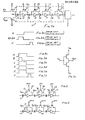
- In order to assist in describing the Prior Art already is referred to Figs. 1a-1b and 2a-2c of the accompanying drawings, where:
- Fig. 1a is a schematic diagram of a comparator employing series-connected single-ended gain stages; Fig. 1b is a schematic diagram of a typical prior art CMOS inverter; and Figs. 2a-2c are the timing diagrams for the clocking signals of the prior art technique for utilizing the circuit of Fig. 1a.
- One technique for reducing offset in a high resolution comparator is to build a comparator which uses a series of cascaded inverter stages. The structure of such a comparator is shown in Fig. la. This type of comparator and its conventional method of operation are described in S.W. Chin, et al., "Charge Balancing is Key to 10-bit A-D Converter Chip", Electronics, October 6, 1981, p. 136 and specification sheet, National Semiconductor ADD3500/ADD3501 3 1/2 Digit DVM With Multiplexed 7-Segment Output, which are hereby incorporated by reference. In operation, as the clocking signals A and A vary with time, the comparator circuit presents a differential voltage, Vin minus Vref' on node 100. Depending upon the relative values of Vin and Vref this differential voltage, however small, will be positive or negative. The differential voltage is held on capacitor 12 and at an appropriate time is amplified by the
successive inverter stages memory device 20 will hold a positive or negative voltage which will unequivocally signify a digital "one" or a digital "zero" depending upon the sign of the differential voltage Vin-Vref. Memory device 20 is interrogated by signal F at an appropriate time in the cycle to obtain an output reading of the comparison. The deficiency with this circuit is that for each inverter stage there is an error charge presented at the input of the stage prior to amplification due to, for example, the voltage feedthrough from the clock to the input lead of the amplifying stages (through capacitance formed between the gate and the source/drain regions of the transistors 21-24). This error charge is amplified by succeeding stages and produces a significant cumulative error that can result in a false comparison. The most significant contribution to the cumulative error is made by the first gain stage (inverter 13, switching transistor 21) because the error is fully amplified by succeeding stages and because the impact of the offsets of subsequent gain stages are reduced by the gain provided by the first stage. In any event, the cumulative error prevents a high resolution comparison from being carried out. - It is therefore an object of the present invention to provide a method and structure for obtaining high resolution comparison using single-ended gain stages.
- It is a further object of the present invention to provide a sequence of operation for a high resolution comparator employing single-ended gain stages whereby the first gain stage is made to appear free of offset error and subsequent gain stages have little impact on the comparison due to the reduction of their offset contribution by the open loop gain of the first stage.
- It is another object of the present invention to provide a method of operating a comparator employing series-connected single-ended gain stages which turns the first stage on in advance of successive stages to null out the offset in the first stage.
- A method of operation is provided for a fast comparator containing multiple series-connected single-ended gain stages. The offset voltage of the first gain stage is cancelled. This serves to reduce the offset of the succeeding gain stages by the open loop gain of the first stage. In other words, by cancelling the offset voltage of the first stage, the differential input voltage which will produce an output voltage of zero is brought much closer to zero, as desired.
- In operation, the switching transistor of the first gain stage is turned off to activate the first inverter stage while the switching transistors of subsequent stages remain on so that the input leads of the inverters are being brought to their initial condition. This serves to eliminate the offset error of the first stage. Subsequently, when the remaining stages are operated to amplify the differential input signal their contributions to offset error are small because their errors are not amplified by the large open loop gain of the first stage (whose offset has already been eliminated). High resolution comparisons may thus be made between an input voltage and a reference voltage.
- For a more complete understanding of the method and structure of the present invention reference may be had to the accompanying drawings which are incorporated herein by reference and in which:
- Fig. la is a schematic diagram of a comparator employing series-connected single-ended gain stages;
- Fig. lb is a schematic diagram of a typical prior art CMOS inverter;
- Figs. 2a-2c are the timing diagrams for the clocking signals of the prior art technique for utilizing the circuit of Fig. la;
- Figs. 3a-3f are the timing diagrams for the operation of the circuit of Fig. 1. in accordance with the method of the present invention;
- Fig. 4 is a schematic diagram of a portion of the circuit of Fig. la illustrating the interrelationship of the states of the first stage and subsequent stages in accordance with the method of the present invention; and
- Fig. 5 is another partial schematic view of the circuit of Fig. la illustrating the contribution o error charge to offset.
- Single-ended gain stage comparators are fast, have no common mode signal restrictions, require small areas when fabricated as a single or part of a larger integrated circuit device, and are inherently stable. However, offset voltage errors remain a problem. Previous attempts to reduce voltage offset have been ineffective because of the clock feedthrough problem as previously described. See, e.g., A. Dingwall, "Monolithic Expandable 6 Bit 20MHz CMOS/SOS A/D Converter", IEEE Journal of Solid State Circuits, December 1979, p. 926, which is hereby incorporated by reference.
- The conventional operation of a comparator 10 having a succession of single-ended gain stages may be understood with reference to the circuit schematic of Fig. la in connection with the timing diagrams of Figs. 2a-2c. As shown in Fig. 2b the clocking signals B, C, D, and E are high to keep switching transistors 21-24 on so as to short the input leads with the output leads of the gain stages 113, 115, 117, and 119 (which include inverting
amplifiers - Clocking signals B, C, D and E then go low thereby turning off switching
transistors amplifiers amplifier 13, g 15 is the gain ofamplifier 15, g17 is the gain ofamplifier 17, and g19 is the gain ofamplifier 19. For eachstage 113, 115, 117, 119 there is an offset error introduced by the spurious current and capacitive coupling between the gates and sources/drains of the switching transistor 21-24 as well as due to component mismatches within theinverters inverter - As shown in Fig. 2a the clocking signal A then goes high to turn on input transistor 11 (and turn off transistor 9) so that the input voltage Vin is presented at node 100. This charges capacitor 12 so that the voltage presented to the input lead of
integrator 13 is the difference voltage, Vin-Vref. The function of the comparator 10 is to produce the difference voltage Vin - Vref and amplify it so it can be detected. When the voltage Vin is close to the reference voltage, Vref, the difference voltage Vin-Vref will be small. It is desired that the change in polarity of the difference voltage, i.e., the crossover of Vin and Vref, be detected as soon as it occurs. It can be seen that the inclusion and amplification of the offset voltages will seriously impede the precise detection of the crossover of Vin and Vref' See S. W. Chin, et al., "Charge Balancing is Key to 10-Bit A-D Converter Chip", Electronics, October 6, 1981, p. 136, which is hereby incorporated by reference. - The present invention employs a unique method of sequencing the clock pulses of the switching
transistors - The method of the present invention may be understood with reference to Fig. la and the timing diagrams of Figs. 3a-3f. To initialize (reset) the comparator, clock signals A, B, C, D and E are initially high. During this initialization period the input voltage Vin is impressed on node 100 via transistor 11. Simultaneously, initializing conditions are established on the
inverters stages 113, 115, 117, and 119) becausetransistors inverters transistor 21 of thefirst stage 13 before the switching transistors of the succeeding stages turn off. The offset of the first stage is zeroed out, i.e., is made to disappear insofar as the succeeding series-connected single-ended gain stages are concerned since they are still in the reset mode. At this time, VB13+g13Voff1 is presented to the input lead of thesecond stage 115, where Voff1 is the offset voltage due to error charge which would appear on the input lead of inverter stage 113, VB13 is the output voltage frominverter 13 during reset, and g13 is the gain of the first stage. However, thesecond stage 115 cannot sense this voltage change (from VB13 to VB13+ g 13 V offl) because thesecond gain stage 115 is still being initialized. This may be seen in the partial schematic diagram of Fig. 4 where the gating signal B for switchingtransistor 21 is indicated to be off while the gating signals C, D for switchingtransistors inverters gain stage 115 and 117. For the first inverter stage 113, however, sincetransistor 21 is off, the voltage appearing on the input lead ofinverter 13 is the offset voltage Voff1 having contributions from the leakage throughtransistor 21. Since thesecond inverter stage 115 is being initialized, however, the amplified output voltage g13 Voff1 which is presented to the second stage is nulled out insofar asinverter 15 is concerned, i.e., makes no contribution to the self-bias voltage V B15. If, as in the prior art, the switchingtransistors transistors - Next, clock signals A, C, D and E go low (as shown in Figs. 3a-3f) so that switching
transistors switches Amplifier 13 amplifies this signal and presents a signal change signal to αg13 (Vref-Vin) to the input lead of thesecond stage 15, where a is the attenuation through capacitor 12. Thesecond stage 15 only amplifies input voltage changes with respect to its input voltage immediately after clock C goes low. In this case this voltage is

- The second stage amplifies the difference voltage between equations (1) and (2), i.e., α(Vref-Vin)g13. Of importance, this is free of first stage offset error Voff13. The
second stage 15 now amplifies α(Vin-Vref)g13 with offset error Voffl5 fromstage 15 only. Similarly, stages 17 and 19 amplify the input differential signal, together with offset voltages from preceeding stages other thanstage 13. However, when the output error is referred back to the input of comparator 10 (offset voltages are always input referred), they are reduced by the gain of the first stage and are no longer significant. In other words, the input voltage which will provide an output signal indicating that Vin-Vref will be made closer to Vref as compared with prior art comparators. For example, using the prior art clock switching technique (clocks B, C, D, and E go low simultaneously), an input offset error voltage Vinoff is present such that an input voltage (Vref+Vinoff) is required to provide an output signal indicating that the input voltage equals the referred Vref' Using the clock switching technique of this method, the input offset error is reduced by the gain g13 of thefirst inverter 13. Thus, in accordance with this invention, an input voltage (Vref+Vinoff/g13) is required to provide an output signal indicating that this allowsmuch more accurate voltage comparisons to be made than was allowed using prior art comparators. - There are two features of the method of the present invention which produce the reduction of offset. First, since the timing signal on the switching transistor of the first stage 113 or another upstream stage is low while both the input transistor 11 and the switching transistors of succeeding gain stages are on, the first stage is made to appear error free. Any leakage current or any circuit-based offset is amplified through the first stage and cancelled out in the closed loop succeeding gain stages. Referring to Figs. 4 and 5, when clock signal B goes low, the output voltage of
inverter 13 is V B13 +g13 V offl3' where Voffl3 is the net change in voltage at node b due to clock signal B going low. The voltage VB13 appears because that is the initializing voltage. Next, when clock A goes low, node 100 changes by Vin-Vref. This causes a change α(Vin-Vref) onnode 101. Thus, the total output voltage ofinverter 13 is VB13+g13Voff13+α(Vin-Vref)g13. Thus the change in output voltage ofinverter 13 is
- where VB13 = self-bias voltage on
first gain stage 13 - Voff13 = offset voltage for first gain stage
- g13 = gain of first stage
- Vin = input voltage
- Vref = reference voltage
- ∞ = attenuation through input capacitor 12.
- Thus, it can be seen that as the comparison of the input voltage Vin takes place, i.e., when the difference voltage Vin-Vref is amplified, there is no contribution of an offset error from the first stage 113 but only an amplification of the potential difference Vin-Vref. Thus there is no offset voltage error from the first stage 113 to be multiplied by
successive stages 115, 117, 119. The second feature that reduces offset for the method of the present invention is that the errors which will be present in the succeedingstages inverter 15 and thus of thesecond gain stage 115. This same principle applies to the offset ofinverter 17 where the effective offset is Voff19/g13g15 where Voff17 is offset of thethird gain stage 17 and forinverter 19 where the effective offset is Voff19/g13g15g17 where Voff19 is the offset of thefourth gain stage 19. Thus, even though there will be offsets for these succeeding stages, the offsets will have minimal impact on the overall comparison of the input voltage Vin with reference voltage Vref' - The method of the present invention has been described in connection with the preferred embodiment in which the first gain stage is placed in an open loop mode in advance of the remaining stages. Additional advantages of a lesser order still accrue if any stages before the final stage are placed in an open loop mode ahead of the following stages. For example, in one embodiment of the present invention, clocking pulse C turned switching
transistor 22 off in advance of clocking pulses D and E. - The specific embodiments of this invention described in this specification are intended to serve by way of example and are not a limitation on the scope of my invention. Numerous other embodiments of this invention will become apparent to those of ordinary skill in the art in light of the teachings of this specification.
- The figures used in the claims are only meant to explain more clearly the intention of the invention and are not supposed to be any restriction concerning the interpretation of the invention.
Claims (8)
Applications Claiming Priority (2)
| Application Number | Priority Date | Filing Date | Title |
|---|---|---|---|
| US55916483A | 1983-12-07 | 1983-12-07 | |
| US559164 | 1983-12-07 |
Publications (2)
| Publication Number | Publication Date |
|---|---|
| EP0145100A2 true EP0145100A2 (en) | 1985-06-19 |
| EP0145100A3 EP0145100A3 (en) | 1987-04-22 |
Family
ID=24232526
Family Applications (1)
| Application Number | Title | Priority Date | Filing Date |
|---|---|---|---|
| EP84201816A Withdrawn EP0145100A3 (en) | 1983-12-07 | 1984-12-06 | Offset reduction for fast comparators employing series-connected, single-ended gain stages |
Country Status (3)
| Country | Link |
|---|---|
| EP (1) | EP0145100A3 (en) |
| JP (1) | JPS60151564A (en) |
| CA (1) | CA1211166A (en) |
Cited By (3)
| Publication number | Priority date | Publication date | Assignee | Title |
|---|---|---|---|---|
| DE3604740A1 (en) * | 1985-02-26 | 1986-09-04 | Mitsubishi Denki K.K., Tokio/Tokyo | Comparator of the chopper type |
| US5065045A (en) * | 1990-10-04 | 1991-11-12 | Atmel Corporation | Multistage offset-cancelled voltage comparator |
| EP0637135A1 (en) * | 1993-07-30 | 1995-02-01 | Seiko Instruments Inc. | Comparator circuit and method of controlling comparator circuit |
Families Citing this family (1)
| Publication number | Priority date | Publication date | Assignee | Title |
|---|---|---|---|---|
| US5365189A (en) * | 1993-03-17 | 1994-11-15 | The Governors Of The University Of Alberta Intellectual Property & Contracts Office University Of Alberta | Drift free low noise composite amplifier and method of operation thereof |
Citations (3)
| Publication number | Priority date | Publication date | Assignee | Title |
|---|---|---|---|---|
| US3676702A (en) * | 1971-01-04 | 1972-07-11 | Rca Corp | Comparator circuit |
| WO1983003932A1 (en) * | 1982-04-23 | 1983-11-10 | Motorola, Inc. | A switched capacitor comparator |
| JPS59133725A (en) * | 1983-01-21 | 1984-08-01 | Hitachi Ltd | Voltage comparator |
-
1984
- 1984-11-22 CA CA000468415A patent/CA1211166A/en not_active Expired
- 1984-12-06 EP EP84201816A patent/EP0145100A3/en not_active Withdrawn
- 1984-12-07 JP JP25776484A patent/JPS60151564A/en active Pending
Patent Citations (3)
| Publication number | Priority date | Publication date | Assignee | Title |
|---|---|---|---|---|
| US3676702A (en) * | 1971-01-04 | 1972-07-11 | Rca Corp | Comparator circuit |
| WO1983003932A1 (en) * | 1982-04-23 | 1983-11-10 | Motorola, Inc. | A switched capacitor comparator |
| JPS59133725A (en) * | 1983-01-21 | 1984-08-01 | Hitachi Ltd | Voltage comparator |
Non-Patent Citations (2)
| Title |
|---|
| IEEE JOURNAL OF SOLID-STATE CIRCUITS, vol. SC-17, no. 6, December 1982, pages 1080-1087, IEEE, New York, US; D.J.ALLSTOT : "A precision variable-supply CMOS comparator" * |
| PATENTS ABSTRACTS OF JAPAN, vol. 8, no. 261 (E-281)[1698], 30th November 1984; & JP-A-59 133 725 (HITACHI) 01.08.1984 * |
Cited By (4)
| Publication number | Priority date | Publication date | Assignee | Title |
|---|---|---|---|---|
| DE3604740A1 (en) * | 1985-02-26 | 1986-09-04 | Mitsubishi Denki K.K., Tokio/Tokyo | Comparator of the chopper type |
| US5065045A (en) * | 1990-10-04 | 1991-11-12 | Atmel Corporation | Multistage offset-cancelled voltage comparator |
| EP0637135A1 (en) * | 1993-07-30 | 1995-02-01 | Seiko Instruments Inc. | Comparator circuit and method of controlling comparator circuit |
| US5565800A (en) * | 1993-07-30 | 1996-10-15 | Seiko Instruments Inc. | Comparator circuit and method of controlling comparator circuit |
Also Published As
| Publication number | Publication date |
|---|---|
| CA1211166A (en) | 1986-09-09 |
| EP0145100A3 (en) | 1987-04-22 |
| JPS60151564A (en) | 1985-08-09 |
Similar Documents
| Publication | Publication Date | Title |
|---|---|---|
| US5410195A (en) | Ripple-free phase detector using two sample-and-hold circuits | |
| US4539551A (en) | Differential voltage amplifier | |
| US5541538A (en) | High speed comparator | |
| US4075509A (en) | Cmos comparator circuit and method of manufacture | |
| US4748418A (en) | Quasi auto-zero circuit for sampling amplifiers | |
| JPH0322103B2 (en) | ||
| US5381053A (en) | Voltage comparator circuit capable of avoiding erroneous operation | |
| US4450368A (en) | AC Coupled chopper stabilized differential comparator | |
| EP0591868A2 (en) | Analog-to-digital converter | |
| EP0090349A1 (en) | Voltage comparator circuit | |
| US5311085A (en) | Clocked comparator with offset-voltage compensation | |
| US4255715A (en) | Offset correction circuit for differential amplifiers | |
| EP0407859B1 (en) | High speed auto zero comparator | |
| US4523107A (en) | Switched capacitor comparator | |
| US5525920A (en) | Comparator circuit and method thereof | |
| EP0145100A2 (en) | Offset reduction for fast comparators employing series-connected, single-ended gain stages | |
| EP0465249B1 (en) | Voltage comparator with sample hold circuit and its use in an analog-to-digital converter | |
| JPH0423333A (en) | Charge transfer device | |
| US4195266A (en) | Commutating signal level translator | |
| JPS6365172B2 (en) | ||
| JPH043520A (en) | Comparator | |
| US5892374A (en) | Latching comparator with input offset adjustment | |
| JPS60229420A (en) | Noise suppressing interface circuit for nonsuperposed 2-phase timing signal generator | |
| US5113091A (en) | Apparatus and method for comparing signals | |
| Habekotte et al. | A smart digital-readout circuit for a capacitive microtransducer |
Legal Events
| Date | Code | Title | Description |
|---|---|---|---|
| PUAI | Public reference made under article 153(3) epc to a published international application that has entered the european phase |
Free format text: ORIGINAL CODE: 0009012 |
|
| AK | Designated contracting states |
Designated state(s): AT DE FR GB IT NL SE |
|
| PUAL | Search report despatched |
Free format text: ORIGINAL CODE: 0009013 |
|
| AK | Designated contracting states |
Kind code of ref document: A3 Designated state(s): AT DE FR GB IT NL SE |
|
| 17P | Request for examination filed |
Effective date: 19871015 |
|
| 17Q | First examination report despatched |
Effective date: 19880729 |
|
| STAA | Information on the status of an ep patent application or granted ep patent |
Free format text: STATUS: THE APPLICATION IS DEEMED TO BE WITHDRAWN |
|
| 18D | Application deemed to be withdrawn |
Effective date: 19881209 |
|
| RIN1 | Information on inventor provided before grant (corrected) |
Inventor name: HAQUE, YUSUF A. |