EP0136656A2 - A nibble and word addressable memory to accessing consecutive data units for supporting decimal arithmetic operations - Google Patents
A nibble and word addressable memory to accessing consecutive data units for supporting decimal arithmetic operations Download PDFInfo
- Publication number
- EP0136656A2 EP0136656A2 EP84111463A EP84111463A EP0136656A2 EP 0136656 A2 EP0136656 A2 EP 0136656A2 EP 84111463 A EP84111463 A EP 84111463A EP 84111463 A EP84111463 A EP 84111463A EP 0136656 A2 EP0136656 A2 EP 0136656A2
- Authority
- EP
- European Patent Office
- Prior art keywords
- nibble
- address
- small
- memory
- word
- Prior art date
- Legal status (The legal status is an assumption and is not a legal conclusion. Google has not performed a legal analysis and makes no representation as to the accuracy of the status listed.)
- Granted
Links
- 238000012545 processing Methods 0.000 claims abstract description 19
- 230000002401 inhibitory effect Effects 0.000 claims description 4
- 230000004044 response Effects 0.000 claims 5
- 238000000034 method Methods 0.000 abstract description 13
- 238000013461 design Methods 0.000 description 5
- 230000006870 function Effects 0.000 description 5
- 238000006073 displacement reaction Methods 0.000 description 4
- 238000012360 testing method Methods 0.000 description 4
- 238000010586 diagram Methods 0.000 description 3
- 230000000295 complement effect Effects 0.000 description 2
- 238000012986 modification Methods 0.000 description 2
- 230000004048 modification Effects 0.000 description 2
- 230000002093 peripheral effect Effects 0.000 description 2
- 238000012546 transfer Methods 0.000 description 2
- 230000008901 benefit Effects 0.000 description 1
- 230000015572 biosynthetic process Effects 0.000 description 1
- 238000006243 chemical reaction Methods 0.000 description 1
- 230000001419 dependent effect Effects 0.000 description 1
- 238000001514 detection method Methods 0.000 description 1
- 230000000694 effects Effects 0.000 description 1
- 230000010354 integration Effects 0.000 description 1
- 230000007246 mechanism Effects 0.000 description 1
- 229910044991 metal oxide Inorganic materials 0.000 description 1
- 150000004706 metal oxides Chemical class 0.000 description 1
- 239000003607 modifier Substances 0.000 description 1
- 238000002360 preparation method Methods 0.000 description 1
- 230000008569 process Effects 0.000 description 1
- 239000000047 product Substances 0.000 description 1
- 239000004065 semiconductor Substances 0.000 description 1
- 238000012163 sequencing technique Methods 0.000 description 1
- 239000013589 supplement Substances 0.000 description 1
- 239000013598 vector Substances 0.000 description 1
Images


Classifications
-
- G—PHYSICS
- G06—COMPUTING; CALCULATING OR COUNTING
- G06F—ELECTRIC DIGITAL DATA PROCESSING
- G06F9/00—Arrangements for program control, e.g. control units
- G06F9/06—Arrangements for program control, e.g. control units using stored programs, i.e. using an internal store of processing equipment to receive or retain programs
- G06F9/30—Arrangements for executing machine instructions, e.g. instruction decode
- G06F9/30003—Arrangements for executing specific machine instructions
- G06F9/30007—Arrangements for executing specific machine instructions to perform operations on data operands
- G06F9/3001—Arithmetic instructions
-
- G—PHYSICS
- G06—COMPUTING; CALCULATING OR COUNTING
- G06F—ELECTRIC DIGITAL DATA PROCESSING
- G06F9/00—Arrangements for program control, e.g. control units
- G06F9/06—Arrangements for program control, e.g. control units using stored programs, i.e. using an internal store of processing equipment to receive or retain programs
- G06F9/30—Arrangements for executing machine instructions, e.g. instruction decode
- G06F9/30003—Arrangements for executing specific machine instructions
- G06F9/30007—Arrangements for executing specific machine instructions to perform operations on data operands
- G06F9/30025—Format conversion instructions, e.g. Floating-Point to Integer, decimal conversion
-
- G—PHYSICS
- G06—COMPUTING; CALCULATING OR COUNTING
- G06F—ELECTRIC DIGITAL DATA PROCESSING
- G06F9/00—Arrangements for program control, e.g. control units
- G06F9/06—Arrangements for program control, e.g. control units using stored programs, i.e. using an internal store of processing equipment to receive or retain programs
- G06F9/30—Arrangements for executing machine instructions, e.g. instruction decode
- G06F9/38—Concurrent instruction execution, e.g. pipeline or look ahead
- G06F9/3877—Concurrent instruction execution, e.g. pipeline or look ahead using a slave processor, e.g. coprocessor
Definitions
- This invention relates to data processing systems and more specifically to a data processing system which provides for execution of decimal numeric software instructions.
- the other method of representing numbers is to represent them in some type of decimal format.
- the decimal format commonly used is to have each decimal digit represented by four or more bits with the bits being binary encoded to represent the values of 0 to 9 decimal.
- Representing numbers in the decimal format has two disadvantages. First, as the number gets larger, more bits are required to represent a number in a decimal format than in a binary format. Second, performing decimal arithmetic operations is more complex and generally slower than binary operations because there are discontinuities at the boundaries between decimal digits which are not present between binary digits.
- the foregoing object is achieved according to one embodiment of the invention according to one mode of operation thereof, by providing in a data processing system microprocessor, a control area which enables the sequencing of the microprocessor.
- the control area provides a branching microinstruction to the subroutine via a microcommand for enabling the return address of the current operating routine to be stored.
- the microcommand also enables a push-down stack so that the previously stored return addresses are pushed down one level.
- the control area further provides for generating vectored interrupt addresses which correspond to the highest priority non-inhibited pending interrupt.
- These vectored interrupt addresses arc provided to the next address register in place of the address generated by the current microinstruction and the address generated by the current microinstruction is pushed onto the push-down stack one level upon the occurrence of an interrupt.
- the control area Upon completion of a subroutine or an interrupt service routine, the control area provides an address field for enabling a multiplexer (MUX) to select the return address contained in the top of the push-down stack to be provided to the next address register in the control area. This popping of the push-down stack also raises one level the previously stored return addresses.
- MUX multiplexer
- Means are also provided so that if an interrupt occurs when returning from a subroutine or interrupt service routine, the push-down stack is neither popped nor pushed and the vectored address is provided to the next address register as the address of the next microinstruction to be executed.
- the push-down stack is implemented using shift registers.
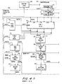
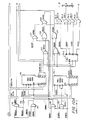
- Figure 1 illustrates the overall data processing system in which the present invention may be used. More particularly, Figure 1 shows a main memory subsystem 10, a central processing unit (CPU) 20 and an input/output (I/O) unit 40.
- the main memory subsystem 10 consists of three metal oxide semiconductor modules 12, 14 and 16. The three modules are interfaced to the central processor unit 20 and the input/output unit 40 via main bus 26.
- the main bus 26 gives the capability of providing access to and control of all memory modules and input/output units.
- the central processing unit 20 executes word oriented software instructions that operate on fixed and variable length fields.
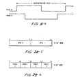
- the basic unit of information in the central processor is a 16-bit word consisting of two 8-bit bytes (see Figure 5).
- a 16-bit word can also be broken into four 4-bit nibbles (see Figure 6).
- These words of information are used in groups of one, two or more for basic instructions (see Figure 7 for an example of one of the instruction formats) or fixed or floating point binary operands (data).
- These words are also used in groups of one or more words for commercial instructions (see Figures 8C-1 tnru 8C-3).
- Bytes are also used in variable length fields as decimal or alphanumeric operands (data).
- CPU 20 is comprised of microprocessor (MPU) 30, monitor logic 22, Read Only Storage (ROS) 24 and commercial instruction logic (CIL) 28.
- Microprocessor 30 is an NMOS, 16-bit chip capable of arithmetic, logic, and control operations, driven by a 48-bit external microinstruction words which in the preferred embodiment are contained in ROS 24.
- the MPU 30 design permits the execution of the CPU 20 basic software instruction repertoire which operates on fixed and floating point binary data.
- Commercial instruction logic (CIL) 28 is used in conjunction with MPU 30 to permit the execution of the CPU 20 commercial software instruction repertoire which operates on decimal and alphanumeric data with the MPU 30 under the control of bits 0-47 of a 56-bit external microinstruction word contained in ROS 24.
- Microprocessor 30 is designed to directly control input/output (I/O) and memory operation for ease in integrated system designs.
- the MPU 30 design permits greater control and integration by use of a 48-bit external microinstruction word that provides true horizontal microprogramming allowing up to 12 simultaneous micro-operations per 48-bit microinstruction word.
- the MPU 30 design also permits 8 external hardware interrupts which generate vectors to microprogram routines as well as allowing 5 external software interrupts that are handled under firmware control.
- MPU 30 provides for 10 external monitor bits originated in monitor logic 22 that are sensed and controlled by sophisticated test branch and major branch operations by logic within microprocessor control area 36 which allows for sophisticated branching operations to be performed within the firmware. Four of these ten external monitor bits are set by CIL 28 to control test branch and major branch operations of MPU 30 when it and CIL 28 are used together to execute a commercial software instruction of CPU 20.
- Microprocessor 30 is comprised of 5 major internal hardware logic areas as shown in Figure 1.
- the five major logic areas are the data manipulation area 32 which includes the arithmetic logic unit (ALU), the memory management unit (MMU 34), the control area 36, the processor bus 37, and internal bus 38.
- ALU arithmetic logic unit
- MMU 34 memory management unit
- control area 36 the control area 36
- processor bus 37 the processor bus 37
- internal bus 38 internal bus
- the bus 37 consists of 20 address/data lines, one memory address violation line and three general purpose control lines. Bus 37 is connected to main bus 26 and is used to provide addresses to the main memory 10 and input/output unit 40 and to receive and send data to main memory 10 and input/output unit 40.
- Internal bus 38 is the major path for communications of information between the other four areas of the microprocessor chip. Internal bus 38 is 20-bit wide. There are 12 sources of information to internal bus 38 under control of the 11 micro-ops within the 48-bit microinstruction word. The ALU is the default source to internal bus 38 if none of the eleven defined micro-ops are used.
- the data manipulation area 32 performs arithmetic and logic operations on data and does memory address generation.
- the control area 36 of MPU 30 is logically divided into 3 areas: input latches for control, testable registers, and the next address generation.
- the MMU 34 section of MPU 30 is comprised primarily of: a register file, a 12-bit address for base relocation, a 9-bit comparator for checking the size of a memory segment, several 2-bit ring comparators for evaluating access rights to a given segment, and storage flip-flops for indicating potential memory violations.
- the MMU 34 translates the software logical address containing a segment number, a block number and an offset value presented by internal bus 38 into a physical address which is placed on bus 37 which in turn is transmitted to main memory 10 via main bus 26.
- CPU 20 executes software programs, the instructions of which are fetched from main memory 10, and performs arithmetic and logical operations on data also contained in main memory 10.
- the software program executed by CPU 20 has the ability to manipulate general and base address registers that are software visible and the current software instruction is pointed to by a program counter. These general registers, base address registers and program counter, which are visible to the software being executed by CPU 20, are physically contained within the data manipulation area 32 of MPU 30.
- CPU 20 of Figure 1 Detailed operation of CPU 20 of Figure 1 is controlled by MPU 30 under the control of microinstructions stored in ROS 24.
- Each location in ROS 24 can be interpreted as controlling one microprocessor machine cycle.
- the contents are decoded by control area 36 resulting in a specific operation within MPU 30.
- microinstruction sequences are obtained that can perform a specific operation or software instruction associated with CPU 20.
- certain bits within the operation code field of the software instruction are used to determine the starting address of the microinstruction routine contained within ROS 24.
- MPU 30 The testing of certain flip-flops which are set or reset by software instruction decoding done by MPU 30 allow the microprocessor to branch to a more specific microinstruction sequence within ROS 24 when necessary.
- MPU 30 branches to that portion of ROS 24 which contains 56-bit microinstruction words so that bits 0-47 are used to control the operation of microprocessor 30 and bits 48-55 are used to control the operation of CIL 28.
- CIL 28 is described in greater detail with reference to Figure 2 below.
- the input/output controller 42 is that portion of the input/output unit 40 which completes a data path from a peripheral device 44 to main memory 10 via main bus 26. I/O controller 42 provides a path tnru which the peripheral commands are initiated, in addition to controlling resulting data transfers.
- the MPU 30 has the ability to perform various shift operations (i.e., open/closed, arithmetic/logical, left/right) on either 16-bit or 32-bit operands.
- ROS 24 may be a read only memory (ROM) or a random access memory (RAM) or any other form of memory device capable of holding microinstructions.
- the ROS 24 contains the microinstructions (or control words) which are used by MPU 30 and CIL 28 to control the operation of central processing unit and mote particularly to execute the software instructions of CPU 20 . For each microprocessor machine cycle, a control word is fetched out of ROS 24.
- ROS 24 is coupled to a ROS data register which receives bits 0 - 47 of the microinstruction word fetched from read only storage 24.
- Each microinstruction contains an address portion and a command portion.
- the address portion in the m i cr oinstruction word identifies the address of the next location to be read from read only storage 24 which will be the next m icroinstruction to be executed by MPU 30.
- the command portion of the microinstruction identifies the operations to be performed by the MPU 30 and CIL 28 during the execution of the current microinstruction.
- the address portion of the microinstruction word may be contained in a predetermined number of bits, for example, in the preferred embodiment it is contained in bits 0 thru 12 of the m i c roinstruction word (see Figure 3).
- the command portion of the microinstruction may also be contained in a predetermined number of bits, for example, in the preferred embodiment it is contained in bits 13 thru 47 which control the operation of MPU 30 and in bits 48 thru 55 which, when present, along with bits 35 thru 47 control the operation of CIL 28 (see Figure 3).
- the command portion may be further broken down into a number of fields which comprise subcommands of the microinstruction.
- FIG 3 illustrates the microinstruction word fields of MPU 30 of the preferred embodiment.
- This microinstruction word is comprised of 56 bits (bits 0-55). Bits 0-47 which control MPU 30 will be discussed now and bits 48-55 which control commercial instruction 28 will be discussed later with reference to Figure 2.
- Bits 0 thru 12 are used as the ROS address field
- bits 13 thru 17 are used to select registers in a register file
- bits 18 thru 22 are used to control the arithmetic and logic functions of the ALU and the inputs to its ports
- bits 23 thru 25 are used as bus control
- bits 26 thru 30 are used as a register modification field
- bits 31 thru 33 are used as memory management unit control
- bit 34 is used to inhibit the occurrence of a hardware interrupt
- bits 35 thru 47 are used as a special control field.
- the special control field (RDDT bits 35 thru 47) is used to modify as well as supplement certain of the other fields in the microinstruction word.
- the special control field provides up to three simultaneous microcommands during a given microcycle.
- the special control field is divided into 4 subfields (A thru D) as illustrated in Figure 3. With the interpretation of some of the subfields dependent upon the contents of other subfields.
- the 48 bits of the microinstructions are loaded into the ROS data register at the beginning of the execution of the microinstruction. These 48 bits are referred to as signals RDDTOO thru RDDT47.
- the ROS address field contains 13 bits (RDDTOO thru RDDT12) and is used to generate the address of the next firmware step in a given microprogram sequence.
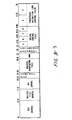
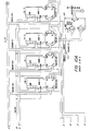
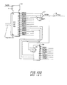
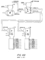
- Figure 2 illustrates the CIL 28, of Figure 1 in greater detail.
- Figure 2 also illustrates MPU 30, read-only storage 24 and monitor logic 22.
- the number next to the upper right-hand corner of the blocks represents the number of bits of information contained in the register represented by the block and the numbers within parentheses next to signal lines represents the number of parallel signals transmitted over the signal path.
- CIL 28 is used in conjunction with MPU 30 to perform the commercial software instructions of CPU 20 which do decimal arithmetic operations on decimal data and editing operations on alphanumeric data strings.
- CIL 28 consists primarily of random access memory (RAM) 1 81, RAM 2 96 and decimal adder/subtractor PROM (DALU) 84, all of which operate under the control of CIL control area 100.
- RAM random access memory
- DALU decimal adder/subtractor PROM
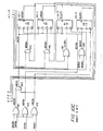
- CIL control area 100 is used to decode the bits within the microinstruction word which control CIL 28.
- CIL control area receives bits 35 thru 47 of the microinstruction word shown as the special control field in Figure 3, which are also used to control the operation of MPU 30 and in addition it receives bits 48 thru 55 which are ''dicated to the contrcl of CIL 28 Decoding of these microinstruction bits associated wich the commercial instruction logic is performed by CIL control area 100 which produces control signals which are distributed thruout CIL 28 to control the enabling and disabling and the selection of the various registers, gates and multiplexers.
- Data is transmitted between microprocess 30 and CIL 28 over a 16-bit wide data path which connects bus 37 of MPU 30 to transceivers (XCVR) 97.
- XCVR transceivers
- the output of XCVR 97 can be latched into data-in register 98 which is also 16 bits wide.
- XCVR 97 can not only load data-in register 98 from the output of bus 37, but can also be used to transfer the output of RAM 2 data register 88 from XCVR 97 to bus 37.
- This data path from the output of RAM 2 data register 88 which is 16 bits wide, besides being connected into XCVR 97 can also be used to load data-in register 98 and thereby provide the means for loading the output of RAM 2 96 into RAM 1 81 or back into RAM 2 96.
- CIL 28 is used to perform a commercial software instruction which requires two operands, operand 1 is usually stored in RAM 1 81 and operand 2 is stored in RAM 2 96 and the output of the operation is stored back into RAM 2 96.
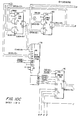
- DALU 84 As indicated, the arithmetic and logic unit functions of CIL 28 are performed by DALU 84.
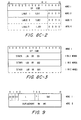
- DALU 84 generates the result by using its four inputs (2 4-bit operands, 1 bit of carry-in and a 1-bit indicator indicating whether this is an add or subtract operation) to form a 10-bit address which is used to fetch and 8-bit data word which contains a 4-bit arithmetic result of the addition or subtraction and four indicators (one bit of carry-out, one bit to indicate whether one of the operands is an illegal value, a bit indicating whether the result is equal to zero, and a bit indicating whether the result is equal to nine).
- Table 1 The coding of DALU 84 is shown in Table 1.
- Table 1 shows the encoding of the 10-bit address.
- the most significant bit in the 10-bit address which has a value of 512, is used as an indicator as to whether the operation being performed is an addition or subtraction.
- address bit 512 is equal to a binary ZERO
- a subtraction is to be performed
- binary ONE an addition is to be performed.
- the next address bit having a value of 256, is used to indicate whether a carry in from the previous decimal digit is to be used in calculating the result and when a binary ZERO indicates that the previous digit did not generate a carry-out and when a binary ONE indicates that the previous digit did generate a carry-out.
- the next four address bits bits having a value of 128, 64, 32 and 16, are used to represent the four bits of operand 2 at the B port of DALU 84 and the last four bits having values of 8, 4, 2 and 1 are used to indicate the values of operand 1 at the A port of DALU 84.
- the 8-bit data word retrieved form PROM 1 as addressed by the 10-bit address is coded with the result as indicated in Table 1.
- the four lower bits of the data word (bits 3 thru 0) contain the 4-bit decimal result of the addition or subtraction.
- the other four bits of the data word contain the four indicators which are output by DALU 84.
- the 4-bit indicators are encoded such that bit 7 of the data word (labeled "CRO" in Table 1), when a binary ZERO, indicates tnat there is no carry-out and, when a binary ONE, indicates that there was a carry-out.
- Bit 6 when a binary ZERO, indicates that both operand 1 and operand 2 were legal decimal values and when a binary ONE, indicates that one or the other of operand 1 or operand 2 contained an illegal decimal value (i.e., a hexadecimal value of from A thru F)
- bit 5 (labeled “EO” in Table 1) indicates when a binary ONE that the arithmetic result is equal to zero and when a binary ZERO that the arithmetic result is not equal to zero
- bit 4 (labeled "E9” in Table 1) when a binary ONE indicates that the arithmetic result equal nine and when a binary ZERO indicates that the arithmetic result does not equal nine.
- the four indicator bits are held by indicators 85 and are also an input into monitor MUX 80 and the carry-out bit is input into DALU 84 as the carry-in bit.
- the 4-bit decimal arithmetic result is one input into result/zone MUX 91.
- the ability to detect whether either of the two operands contains a value greater than 9 is very useful in that it allows the DALU 84 to detect the case of an illegal operand which has a decimal digit which is represented by four bits and therefore can have values of from A thru F hexadecimal which are illegal.
- the ability for the DALU 84 to detect illegal decimal operands as part of the addition/subtraction process eliminates the need for a separate precheck of the operands by a prescan of the operands prior to introducing them into the ALU.
- Sign detector PROM 78 is similar in operation to DALU 84. Sign PROM 78 uses the nine input bits to address a 4-bit data word which indicates the sign of the operands used in an arithmetic operation. Of the nine bits used to address the 4-bit data words of the PROM 78, three bits come from data-in register 98, 4 bits from sign multipliexer 77, and two bits (PACKD) and overpunch (OVPUN) from CIL control area 100. The output of PROM 78 can be gated to monitor logic 22 for inputing into MPU 30 via monitor MUX 80.
- the four bits output by PROM 78 indicate whether the sign is positive or negative, whether it is an illegal sign atom, whether the sign is an overpunch sign, and whether it is an overpunched zero.
- the resultant sign can be tested by the MPU 30 firmware examining the four monitor bits.
- the generation of the sign result is complex in that the CPU 20 allows decimal numbers to be represented in either a packed or unpacked format with trailing or leading signs and overpunch signs.
- RAM 1 zero MUX 82 at the output of RAM 1 81 and RAM 2 zero MUX 90 at the output of RAM 2 96 are used to allow the commercial instruction logic firmware to effectively zero out the output of RAM 1 and RAM 2 respectively so that the operand in the other RAM can effectively be added or subtracted from zero.
- RAM 2 data register 88 holds the 16-bit output of RAM 2 96.
- RAM 2 nibble MUX 89 is used to select the one of the four 4-bit nibbles held in RAM 2 data register 88 so that the appropriate nibble can be gated into RAM 2 zero MUX 90 or into double MUX 83 in preparation of adding or subtracting a nibble from RAM 2 96 with a nibble from RAM 1 81 in DALU 84.
- Nibble 0 MUX 92, nibble 1 MUX 93, nibble 2 MUX 94, and nibble 3 MUX 95 are used to either allow a 16-bit quantity to be loaded in from data-in register 98 into RAM 2 96 or to allow a 4-bit nibble from result/zone MUX 91 into the appropriate 4-bit nibble of the 16-bit word stored in RAM 2 96 under firmware control.
- Result/zone MUX 91 is used to determine whether the 4-bit result from DALU 84 or the four zone bits are to be written into a nibble within RAM 2 96.
- each four bits of data in the decimal value represent a decimal digit having the value from zero thru nine.
- each decimal digit is represented by an eight bits in which the most significant (left) four bits of the 8-bit field represent a zone field having a value of 3 hexadecimal and the least significant (right) four bits represent the decimal values 0 thru 9.
- each decimal digit is represented by an 8-bit field which contains the ASCII code for the decimal digit. Therefore, result/zone MUX 91 can select between the 4-bit result from DALU 84 (which can have a value from 0 thru 9) or the four zone bits which are preset to 0011 binary (3 hexadecimal). For example, the decimal value 76 when stored in a packed field is stored in eight bits with the most significant 4-bit nibble containing the value 7 and the least significant 4-bit nibble containing the value 6.
- 76 decimal When the same value of 76 decimal is stored in an unpacked field, it is stored in two 8-bit bytes with the left most 4-bit nibble of each byte being a 4-bit zone field which contains the hexadecimal value of three and the right 4-bit nibble in each byte containing the decimal value of 7 in the left byte and 6 in the right byte. Therefore, the value of 76 decimal in a packed decimal field is represented by the 8-bit field of 76 hexadecimal and in an unpacked field it is represented by a 16-bit field containing 3736 hexadecimal.
- Double MUX 83 allows one input of DALU 84 to be selected between four bits from RAM 1 81 or four bits from RAM 2 96.
- double MUX 83 selects one input of DALU 84 to be four bits from RAM 2 96, the effect is that the output of DALU 84 is double the value of the four bits from RAM 2 because in this case both inputs to the DALU 84 will be from RAM 2. This provides a very convenient method of multiplying by two the operand stored in RAM 2 96.
- RAM 1 81 and RAM 2 96 contain 16-bit data words, with RAM 1 containing 16 such 16-bit words and RAM 2 containing 256 16-bit words, there are other distinctions between these two RAMs.
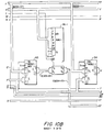
- RAM 1 normally holds operand 1 and may be written into only on a 16-bit word basis. That is, when information is written into RAM 1 from data-in register 98, all four nibbles of the 16-bit word are written to.
- the output of RAM 1 is always a single 4-bit nibble which is presented at one of two inputs to RAM 1 zero M U X 82.
- the word which is read from RAM 1 81 is controlled by RAM 1 address counter 75 and the nibble which is enabled into one input of RAM 1 zero MUX 82 is controlled by nibble out control 76.
- RAM 1 address counter 75 also receives inputs from nibble out control 76 such that consecutive decimal digits maybe accessed from RAM 1 by either incrementing or decrementing a nibble counter in nibble out control 76 which in turn either increments or dectements the word counter in RAM 1 address counter 75 each time that four nibbles have been accessed.
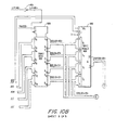
- RAM 2 96 has the ability to be written into as one 16-bit word or the ability to write any one of the four individual nibbles.
- the 16-bit word to be written into RAM 2 96 comes from data-in register 98 which can be loaded from bus 37 or from the output of RAM 2 data register 88.
- Individual nibbles are written into RAM 2 96 from the output of result/zone MUX 91 with the value of the nibble being either the result of the DALU 84 or a 4-bit zone field containing the hexadecimal value of 3.
- Nibble write control 86 determines whether a 16-bit word is written into RAM 2 96 or whether one of four individual nibbles is written into RAM 2 96.
- RAM 2 address counter 87 determines the 8-bit word address that is used to address RAM 2 96 for either a read or write operation.
- RAM 2 address counter 87 receives an input from nibble write control 86 so that consecutive nibbles may be accessed from RAM 2 96. Each time the four nibbles have been accessed, RAM 2 address counter 87 is either incremented or decremented to get to the next word which contains the next consecutive nibble.
- a read from RAM 2 96 results in a 16-bit data word being read out and latched into RAM 2 data register
- RAM 1 31 is used primarily to hold operand 1 which, in the CPU of the preferred embodiment, may be a decimal number of from 1 thru 31 decimal digits including the sign. Therefore, to accommodate a 31 digit decimal number, sixteen words of 16 bits each are required in order to be able to hold the 31 bytes of the maximum decimal number if the number is an unpacked decimal number having zone bits associated with each decimal digit.
- RAM 2 96 besides normally holding operand 2 is divided into eight segments with each segment being used to either hold an operand or as a working register. For example, in the case of a decimal divide, the segments of RAM 2 96 are used to hold an original copy of operand 1, an original copy of operand 2, a packed copy of operand 2, the quotient and partial products.
- microinstruction word which control the operation of CIL 28 will now be described with reference to Figure 2 and Figure 3 and Table 2 thru Table 6.
- a microinstruction word is read from ROS 24 either 48 bits or 56 bits are retrieved. If the address is within the first 2K of ROS (i.e., addressed 0 thru 2047) a 48-bit microinstruction word is retrieved and if the address is from 2048 thru 4095 a 56-bit microinstruction word is retrieved.
- bits 0 thru 47 of microinstruction word are always latched into a ROS data register in control area 36 for decoding and controlling the operations of MPU 30.
- the special control field of the microinstruction word bits 35 thru 47, are also latched into ROS SCF register 101 of CIL control area 100 (see Figure 2).
- subfield A of the special control field is used to enable some of the mops controlled by subfields B and C.
- the requirement that certain of the mops specified in subfields B and C of the special control field are enabled only if subfield A contains a binary 110 is necessary in order to inhibit CIL 28 from performing certain mops which would otherwise interfere with the mops being performed by MPU 30.
- Zero MUX 102 is used to force binary ZEROs into ROS CIL register 103 when the MPU 30 addresses a firmware location in the lower 2K of ROS 24 (see Table 5 and Table 6) thereby inhibiting CIL 28 from performing any operation when a microinstruction word has been retireved from ROS 24 which does not contain bits RDDT48 thru RDDT55 (see Figure 3).
- CIL control area 100 the various control signals from CIL control area 100 are applied to the various logic elements of CIL 28 during each microinstruction execution cycle. It will also be understood that the clock signals from MPU 30 provide appropriate timing signals in a conventional manner to the CIL 28 to provide appropriate timing therefor. In order not to confuse the drawings, the particular timing and control signals fed to various elements are not shown in Figures 1 and 2, but are assumed to be provided where appropriate.
- RDDT42 thru RDDT44 control the following mops.
- a binary 000 no operation is performed by CIL 28.
- the PACKD signal input into sign detection PROM 78 is made a binary ZERO and is used to address the portion of the sign PROM 78 which contains the coding for packed decimal sign types.
- signal OVPUN becomes a binary ZERO and is used to address the portion of the PROM 78 which contains the encoding for overpunched signs.
- DALU 84 When a binary 011, a subtract operation is performed by DALU 84 by forcing the signal ADD/SUB which is one of its inputs to be a binary ZERO.
- the equal zero and equal nine indicators in indicators 85 are reset to zero.
- RAM 1 address counter 75 When a binary 101, the address counter in RAM 1 address counter 75 is incremented by one such that the next word in RAM 1 81 is addressed thereby allowing one of four new nibbles to be input into RAM 1 zero MUX 82.
- the nibble enabled into RAM 1 zero MUX 82 is determined by nibble out control 76.
- RAM 1 address counter 75 When a binary 110, RAM 1 address counter 75 is decremented by one, addressing the next lower word in RAM 1 81 and making available at its output one of four new nibbles with the enabled nibble again being under the control of nibble output control 76.
- all four indicators in decimal indicators 85 are reset to binary ZERO thereby indicating that there is no carry, that the result is not equal to zero, that the result is not equal to nine, and that the result is not an illegal digit.
- the mops controlled by subfield E are illustrated in Table 5.
- nibble write control 86 When a binary 0011, a word address is loaded into RAM 1 address counter 75 and a nibble count is loaded into nibble output control 76 from data-in register 98 thereby allowing the specifying as to the word and the nibble which will be read from RAM 1 81.
- an initial address is loaded into RAM 2 address counter 37 from data-in register 98 thereby controlling which word will be written into or read from RAM 2 96.
- an initial nibble count is loaded into nibble write control 86 thereby controlling which nibble will be write enabled into RAM 2 96.
- the nibble counter within nibble write control 86 also controls which of the four nibbles from RAM 2 data register 88 is enabled onto the outputs of RAM 2 nibble MUX 89.
- the address counter in RAM 2 address counter 87 and the nibble counter in nibble write control 86 are loaded from data in register 98 thereby controlling the word that is addressed within RAM 2 and the nibble which is write enabled into RAM 2 and the nibble which is selected at the output of RAM 2 nibble MUX 89.
- the word address contained in data-in register 98 is loaded into RAM 1 address counter 75 and RAM 2 address counter 87.
- the nibble count and data-in register 98 is loaded into the nibble out control 76 and into nibble write control 86 thereby allowing the selection of one of four nibbles in RAM 1 and RAM 2.
- the word address and the nibble count from data-in register 98 are loaded into RAM 1 address counter 75 and RAM 2 address counter 87 and nibble out control 76 and nibble write control 86 respectively.
- the nibble counter in nibble out control 76 When a binary 1010, the nibble counter in nibble out control 76 is incremented by one and if it changes from a nibble count of three to a nibble count of zero, the word counter in RAM 1 address counter 75 is also incremented by one. This allows nibbles to be consecutively addressed and after the four nibbles have been addressed from one word, the first nibble is addressed in the next word.
- the nibble counter in nibble out control 76 is decremented by one and if the count changes from zero to three, the word counter in RAM 1 address counter 75 is decremented by one thereby allowing consecutive nibbles to be addressed from right to left.
- the nibble counter in write control 86 When a binary 1100, the nibble counter in write control 86 is incremented by one and if the nibble counter goes from three to zero, the word counter in RAM 2 address counter 87 is also incremented by one thereby allowing consecutive nibbles to be addressed from left to right.
- the nibble counter in nibble write control 86 When a binary 1101, the nibble counter in nibble write control 86 is decremented by one and if the count goes from zero to three, the word counter in RAM 2 address counter 87 is also decremented by one to point to the next word in RAM 2 96. This decrementing of the nibble counter associated with RAM 2 by one allows consecutive nibbles in RAM 2 to be addressed from right to left.
- the nibble counter in nibble out control 76 is incremented by one as is the nibble counter in nibble write control 86 and when a counter go from three to zero, the corresponding word counter in RAM 1 address counter 75 and RAM 2 address counter 87 is also incremented by one thereby allowing consecutive nibbles to be addressed from left to right in RAM 1 and RAM 2.
- nibble counter in nibble out control 76 is decremented by one
- the nibble counter in nibble write control 86 is decremented by one
- RDDT52 thru RDDT55 is a binary 0000
- no operation is performed by CIL 28.
- XCVR 97 are enabled such that the data on bus 37 is available to data-in register 98 and data-in register 98 is clocked such that the information becomes available to CIL 28 at the output of data-in register 98.
- the XCVR 97 are enabled to transmit data from CIL 28 to MPU 30 such that the information in RAM 2 data register 98 is passed to bus 37.
- this mop clocks data-in register 98 such that the data from RAM 2 data register 88 is loaded into data-in register 98.
- the word address counter in RAM 2 address counter 87 is incremented by one thereby pointing to the next word within RAM 2 96. It should be noted that the incrementing and decrementing of the address counter for RAM 2 is controlled by subfield F and the incrementing and decrementing of the address counter for RAM 1 is controlled by subfield C so that the address counters of RAM 2 and RAM 1 can be incremented and decremented in parallel.
- the carry indicator in indicators 85 is set to a binary ONE.
- a test mode flop is set to indicate that a fault condition has occurred within CIL 28.
- XCVR 97 are enabled to receive data from bus 37 and data-in register 98 is clocked such that the data is latched in it and at the same time the word address counter in RAM 2 address counter 87 is incremented by one.
- XCVR 97 are enabled to receive the data from bus 37 and it is latched into data-in register 98.
- the address counter in RAM 2 address counter 87 is decremented by one such that the next lower word in RAM 2 96 is addressed. As in the previous mop, it is useful for allowing consecutive words in RAM 2 to be loaded from bus 37.
- XCVR 97 When a binary 1011, XCVR 97 are enabled to transmit the data from the output of RAM 2 data register 88 to bus 37 and at the same time this data is loaded into data-in register 98. In addition, the address counter in RAM 2 address counter 87 is incremented by one. When a binary 1100, XCVR 97 are enabled to to bus 37 to allow the outputting of data in RAM 2 data register 88 and at the same time the data is loaded into data-in register 98. In addition, the address counter in RAM 2 address counter 87 is decremented by one such that the next lower word in RAM 2 96 is pointed to. The mops specified by binary 1101, 1110 and 1111 are not used.
- the three different data types handled by the CIL 28 are: decimal data, alphanumeric data, and binary data.
- the decimal and binary data types are used to represent fixed point integer numeric values.
- the alphanumeric data type is used to represent alphabetic, numeric and punctuation of text information.
- the commercial software instructions of the CPU permit arithmetic operations on the decimal data and editing operations on alphanumeric data. These commercial software instructions are performed by CIL 28 in conjunction with M P U 30.
- Table 7 gives the size of an atom in bits as a function of the data type.
- Eight-bit atoms are also referred to as “bytes” and 4-bit atoms are also referred to as “nibbles”.
- Figure 5 illustrates the position of byte 0 and byte 1 within the 16-bit words of the preferred embodiment.
- Figure 6 illustrates the positions of nibble 0 thru nibble 3 in a 16-bit word.
- the bits are numbered 0 thru 15 with bit 0 being the most significant bit (MSB) and bit 15 being the least significant bit (LSB) as illustrated in Figures 5 and 6.
- Decimal data can be represented in either string (also referred to as unpacked) or packed form.
- the maximum length of a decimal operand is 31 atoms (i.e., if separate sign, then 30 digits plus sign).
- Decimal numbers are treated as integers with the decimal point assumed to be to the right of the least significant digit.
- a decimal operand can be signed or unsigned and when unsigned it is assumed to be positive.
- Zone bits are not checked by the hardware on input but will be set to 3 hexadecimal (0011 binary) on output.
- String decimal data can be signed or unsigned. When unsigned the operand is considered to be positive and its length refers only to digits. When signed, the operand can have either: leading separate sign, trailing separate sign, or trailing overpunched sign.
- the length of the operand also includes the sign character.
- decimal digits occupy four bits or one-half a byte position in memory (also referred to as nibbles). These digits can start and/or end on any half byte boundaries. The only valid codes for packed decimal digits are 0-9 otherwise an illegal character trap will result.
- Packed decimal data can be signed or unsigned.
- the operand When unsigned, the operand is considered to be positive and its length refers only to digits. When signed, the sign will be the least significant atom of the operand. The length of the operand will include the sign atom. Sign, when specified, can only be separate trailing; i.e., the rightmost atom of the operand field.
- Alphanumeric operands consist of ASCII 7-bit characters. Their maximum size is 255 characters except as specified otherwise. Each alphanumeric character atom occupies one 8-bit byte.
- Alphanumeric strings in memory can start and/or end or both on either odd or even byte boundaries.
- Binary operands can be either 16 bits long or 32 bits long (i.e., one or two words). They are 2's complement numbers and thus the most significant bit is the sign bit and the binary point is assumed to be to the right of the least significant bit.
- Binary operands in memory can start and/or end on either odd or even byte boundaries.
- the commercial software instructions of CPU 20 are classified as follows: numeric, alphanumeric, edit and branch.
- a commercial software instruction can have from 1 to 3 operands which are defined by data descriptors.
- Data descriptors DDs are used to define the operand type, size and location in memory.
- Figure 8C-1 illustrates the format of a commercial software instruction using in-line data descriptors which describe the 1 to 3 operands used by the instruction.
- Figure 8C-2 illustrates the format of a commercial software instruction using remote data descriptors and
- Figure 8C-3 shows the format of a commercial software instruction using a combination of in-line and remote data descriptors.
- bits 12 thru 15 are binary ZEROs.
- a data descriptor can be either a: decimal DD, alphanumeric DD, or binary DD.
- Decimal DDs are implied by all numeric software instructions and the numeric edit instruction. Decimal DDs can refer to either string decimal or packed decimal data. The format of the DD is as shown in Figure 9 where:
- Alphanumeric DDs are implied by all alphanumeric software instructions and tne alphanumeric edit software instruction.
- the format of the alphanumeric DD is somewhat similar to that shown in Figure 9 but need not be further described.
- the CAS is a seven bit field of a data descriptor in which bits 9 thru 11 are used as an address modifier, bit 12 is generally used to indicate whether direct or indirect addressing is to be used, and bits 13 thru 15 are used to indicate a base register number.
- the definition of the commercial software instructions supports post indexing of data at the atom level.
- the index value is in atoms and it is automatically adjusted to correspond to the data type specified in the DD.
- Convert binary to decimal moves and converts the contents of binary DD1 and places the decimal string or packed result in the contents of DD2 (i.e., [DDl] converted and stored in [DD2]).
- DD2 i.e., [DDl] converted and stored in [DD2]
- the OV and SF commercial indicators are set as a function of the result.
- Figure 10A primarily shows the structure of RAM 1 31 and its associated addressing logic
- Figure 10B primarily shows the structure of RAM 2 and its associated addressing logic
- Figure 10C primarily shows the structure of DALU 84 along with its inputs and outputs and indicators 85
- Figure 10D primarily shows the structure of CIL control area 100.
- the decimal arithmetic operations that are performed by CPU 20 are microprogrammed to take advantage of CIL 28 to reduce the execution time of the decimal commercial software instructions.
- the convert decimal to binary commercial software instruction is sped up by using the ability to address RAM 1 81 for left to right to strip leading zeros.
- the convert binary to decimal commercial software instruction is sped up by using the ability of the DALU 84 to have the same data fed to both inputs and by presetting the converted value receiving field to a zero digit and increasing the receiving field length as necessary (when a carry occurs) as the conversion progresses.
- microprocessor 30 and CIL 28 operate in parallel to perform the necessary mops under the control of microinstructions stored in ROS 24.
- Microinstruction bits 0 thru 47 are used to control the operation of MPU 30 and microinstruction bits 35 thru 55 be used to control the operation of CIL 28.
- the use of microinstruction bits 35 thru 47 to control MPU 30 or commercial instruction logic 29 depend on the value of special control field subfield A.
- MPU 30 is used to: read the software instructions from main memory 10, to decode the software instructions, to read the operands from main memory 10, to perform arithmetic, shifting and logical operations on binary data, and write the results of the operation back into main memory 10.
- CIL 28 is used to perform logic and shifting operations on decimal and alphanumeric data.
- the commercial instruction logic can be adapted to work on words that have fewer or more than 16 bits and decimal data formats using different representations with different nibbles and atom sizes.
- the commercial instruction logic can be used with the CPU having different microprocessors or combinatorial logic.
- the control of the commercial instruction logic can be done using different mops or combinatorial logic.
- the methods used to perform the various arithmetic operations can be adapted to use different hardware.
Landscapes
- Engineering & Computer Science (AREA)
- Theoretical Computer Science (AREA)
- Software Systems (AREA)
- General Physics & Mathematics (AREA)
- Physics & Mathematics (AREA)
- General Engineering & Computer Science (AREA)
- Mathematical Analysis (AREA)
- Mathematical Optimization (AREA)
- Pure & Applied Mathematics (AREA)
- Computational Mathematics (AREA)
- Executing Machine-Instructions (AREA)
- Memory System (AREA)
- Advance Control (AREA)
- Debugging And Monitoring (AREA)
Abstract
Description
- This invention relates to data processing systems and more specifically to a data processing system which provides for execution of decimal numeric software instructions.
- There are primarily two different methods employed within modern data processing systems for representing numeric data.
- It can be represented in a binary format in which each bit within a word is given a weight of 2 raised to a power such that the least significant bit, when a binary ONE, represents 2 to the zeroth power, the next more significant bit, when a binary ONE, represents 2 to the first power and so on. Negative numbers in a binary format may be indicated by a sign bit at either the beginning or end of the number or by performing a two's complement on the number.
- The other method of representing numbers is to represent them in some type of decimal format. The decimal format commonly used is to have each decimal digit represented by four or more bits with the bits being binary encoded to represent the values of 0 to 9 decimal. Representing numbers in the decimal format has two disadvantages. First, as the number gets larger, more bits are required to represent a number in a decimal format than in a binary format. Second, performing decimal arithmetic operations is more complex and generally slower than binary operations because there are discontinuities at the boundaries between decimal digits which are not present between binary digits.
- Numerous techniques for performing decimal arithmetic operations in data processing systems are known in the prior art. Some tecnniques are described in the book entitled, Digital Computer Design Fundamentals, by Y. Chu, published by McGraw-Hill Book Company Inc., 1962 which is incorporated herein by reference. These techniques generally require that individual decimal digits be manipulated one digit at a time at some point in performing a decimal arithmetic operation.
- Therefore, in order to speed up decimal operations, what is needed are methods to efficiently manipulate individual decimal digits within a data processing system and methods which reduce the number of digits which must be manipulated during any arithmetic operation.
- The foregoing object is achieved according to one embodiment of the invention according to one mode of operation thereof, by providing in a data processing system microprocessor, a control area which enables the sequencing of the microprocessor. The control area provides a branching microinstruction to the subroutine via a microcommand for enabling the return address of the current operating routine to be stored. The microcommand also enables a push-down stack so that the previously stored return addresses are pushed down one level. The control area further provides for generating vectored interrupt addresses which correspond to the highest priority non-inhibited pending interrupt. These vectored interrupt addresses arc provided to the next address register in place of the address generated by the current microinstruction and the address generated by the current microinstruction is pushed onto the push-down stack one level upon the occurrence of an interrupt. Upon completion of a subroutine or an interrupt service routine, the control area provides an address field for enabling a multiplexer (MUX) to select the return address contained in the top of the push-down stack to be provided to the next address register in the control area. This popping of the push-down stack also raises one level the previously stored return addresses. Means are also provided so that if an interrupt occurs when returning from a subroutine or interrupt service routine, the push-down stack is neither popped nor pushed and the vectored address is provided to the next address register as the address of the next microinstruction to be executed. In the preferred embodiment, the push-down stack is implemented using shift registers.
- The manner in which the method of the present invention is performed and the manner in which the apparatus of the present invention is constructed and its mode of operation can best be understood in light of the following detailed description together with the accompanying drawings in which like reference numbers identify like elements in the several figures and in which:
- Figure 1 is a general block diagram of a data processing system utilizing the present invention;
- Figure 2 is a block diagram of the commercial instruction logic of Figure 1 which carries out the principles of the present invention;
- Figure 3 illustrates the microinstruction word fields of the microprocessor of Figure 1 and the commercial instruction . logic of Figure 2;
- Figure 4 illustrates the clock phase relationship of one microinstruction cycle of the microprocessor of Figure 1;
- Figures 5 and 6 illustrate the position of 8-bit bytes and 4-bit nibbles in a 16-bit word of a data processing system utilizing the present invention;
- Figure 7 illustrates the format of a single or double operand basic software instruction processed by the central processing unit of Figure 1;
- Figure 8 illustrates the format of a commercial software branch instruction processed by the central processing unit of Figure 1;
- Figures 8C-1 thru 8C-3 illustrate the format of commercial software numeric, alphanumeric and edit instructions with in-line data descriptors, remote data descriptors and a combination of in-line and remote data descriptors;
- Figure 9 illustrates the format of the data descriptors used by the commercial software instructions of the central processing unit of Figure 1; and
- Figures 10A thru 10D are logic block diagrams of circuitry utilized in the commercial instruction logic of Figure 2 in accordance with the present invention.
- The implementation of the embodiment illustrated in the drawings is effected with a given arrangement of circuitry. However, it is understood that other logic arrangements may be employed in carrying out the invention to adapt the invention to various types of data processors. Accordingly, it is not intended to be limited to the specific schemes shown in the drawings.
- Referring now to the drawings, Figure 1 illustrates the overall data processing system in which the present invention may be used. More particularly, Figure 1 shows a
main memory subsystem 10, a central processing unit (CPU) 20 and an input/output (I/O)unit 40. Themain memory subsystem 10 consists of three metaloxide semiconductor modules central processor unit 20 and the input/output unit 40 viamain bus 26. Themain bus 26 gives the capability of providing access to and control of all memory modules and input/output units. - The
central processing unit 20 executes word oriented software instructions that operate on fixed and variable length fields. The basic unit of information in the central processor is a 16-bit word consisting of two 8-bit bytes (see Figure 5). A 16-bit word can also be broken into four 4-bit nibbles (see Figure 6). These words of information are used in groups of one, two or more for basic instructions (see Figure 7 for an example of one of the instruction formats) or fixed or floating point binary operands (data). These words are also used in groups of one or more words for commercial instructions (see Figures 8C-1 tnru 8C-3). Bytes are also used in variable length fields as decimal or alphanumeric operands (data). -
CPU 20 is comprised of microprocessor (MPU) 30,monitor logic 22, Read Only Storage (ROS) 24 and commercial instruction logic (CIL) 28.Microprocessor 30 is an NMOS, 16-bit chip capable of arithmetic, logic, and control operations, driven by a 48-bit external microinstruction words which in the preferred embodiment are contained inROS 24. The MPU 30 design permits the execution of theCPU 20 basic software instruction repertoire which operates on fixed and floating point binary data. Commercial instruction logic (CIL) 28 is used in conjunction withMPU 30 to permit the execution of theCPU 20 commercial software instruction repertoire which operates on decimal and alphanumeric data with theMPU 30 under the control of bits 0-47 of a 56-bit external microinstruction word contained inROS 24. As will be seen below,ROS 24 contains 2K (where lK = 1024) of 48-bit microinstruction words which are used to execute the basic software instructions ofCPU 20 andROS 24 also contains 2K of 56-bit microinstruction words which are used to execute the commercial software instructions ofCPU 20 with bits 0-47 controllingMPU 30 and bits 48-55 controllingCIL 28. -
Microprocessor 30 is designed to directly control input/output (I/O) and memory operation for ease in integrated system designs. The MPU 30 design permits greater control and integration by use of a 48-bit external microinstruction word that provides true horizontal microprogramming allowing up to 12 simultaneous micro-operations per 48-bit microinstruction word. The MPU 30 design also permits 8 external hardware interrupts which generate vectors to microprogram routines as well as allowing 5 external software interrupts that are handled under firmware control. In addition, MPU 30 provides for 10 external monitor bits originated inmonitor logic 22 that are sensed and controlled by sophisticated test branch and major branch operations by logic withinmicroprocessor control area 36 which allows for sophisticated branching operations to be performed within the firmware. Four of these ten external monitor bits are set byCIL 28 to control test branch and major branch operations ofMPU 30 when it andCIL 28 are used together to execute a commercial software instruction ofCPU 20. -
Microprocessor 30 is comprised of 5 major internal hardware logic areas as shown in Figure 1. The five major logic areas are thedata manipulation area 32 which includes the arithmetic logic unit (ALU), the memory management unit (MMU 34), thecontrol area 36, theprocessor bus 37, and internal bus 38. - The
bus 37 consists of 20 address/data lines, one memory address violation line and three general purpose control lines.Bus 37 is connected tomain bus 26 and is used to provide addresses to themain memory 10 and input/output unit 40 and to receive and send data tomain memory 10 and input/output unit 40. - Internal bus 38 is the major path for communications of information between the other four areas of the microprocessor chip. Internal bus 38 is 20-bit wide. There are 12 sources of information to internal bus 38 under control of the 11 micro-ops within the 48-bit microinstruction word. The ALU is the default source to internal bus 38 if none of the eleven defined micro-ops are used.
- The
data manipulation area 32 performs arithmetic and logic operations on data and does memory address generation. - The
control area 36 ofMPU 30 is logically divided into 3 areas: input latches for control, testable registers, and the next address generation. - The
MMU 34 section ofMPU 30 is comprised primarily of: a register file, a 12-bit address for base relocation, a 9-bit comparator for checking the size of a memory segment, several 2-bit ring comparators for evaluating access rights to a given segment, and storage flip-flops for indicating potential memory violations. During any CPU generated memory address cycle, theMMU 34 translates the software logical address containing a segment number, a block number and an offset value presented by internal bus 38 into a physical address which is placed onbus 37 which in turn is transmitted tomain memory 10 viamain bus 26. - As can be appreciated as the description so far,
CPU 20 executes software programs, the instructions of which are fetched frommain memory 10, and performs arithmetic and logical operations on data also contained inmain memory 10. The software program executed byCPU 20 has the ability to manipulate general and base address registers that are software visible and the current software instruction is pointed to by a program counter. These general registers, base address registers and program counter, which are visible to the software being executed byCPU 20, are physically contained within thedata manipulation area 32 ofMPU 30. - Detailed operation of
CPU 20 of Figure 1 is controlled byMPU 30 under the control of microinstructions stored inROS 24. Each location inROS 24 can be interpreted as controlling one microprocessor machine cycle. As each location ofROS 24 is read, the contents are decoded bycontrol area 36 resulting in a specific operation withinMPU 30. By grouping ROS locations, microinstruction sequences are obtained that can perform a specific operation or software instruction associated withCPU 20. As each software instruction is initiated, certain bits within the operation code field of the software instruction are used to determine the starting address of the microinstruction routine contained withinROS 24. The testing of certain flip-flops which are set or reset by software instruction decoding done byMPU 30 allow the microprocessor to branch to a more specific microinstruction sequence withinROS 24 when necessary. When a commercial software instruction is encountered,MPU 30 branches to that portion ofROS 24 which contains 56-bit microinstruction words so that bits 0-47 are used to control the operation ofmicroprocessor 30 and bits 48-55 are used to control the operation ofCIL 28.CIL 28 is described in greater detail with reference to Figure 2 below. - Connected to
main bus 26 is a input/output unit 40. The input/output controller 42 is that portion of the input/output unit 40 which completes a data path from aperipheral device 44 tomain memory 10 viamain bus 26. I/O controller 42 provides a path tnru which the peripheral commands are initiated, in addition to controlling resulting data transfers. - The
MPU 30 has the ability to perform various shift operations (i.e., open/closed, arithmetic/logical, left/right) on either 16-bit or 32-bit operands. -
ROS 24 may be a read only memory (ROM) or a random access memory (RAM) or any other form of memory device capable of holding microinstructions. TheROS 24 contains the microinstructions (or control words) which are used byMPU 30 andCIL 28 to control the operation of central processing unit and mote particularly to execute the software instructions of CPU 20. For each microprocessor machine cycle, a control word is fetched out ofROS 24. - ROS 24 is coupled to a ROS data register which receives bits 0-47 of the microinstruction word fetched from read only
storage 24. Each microinstruction contains an address portion and a command portion. The address portion in the microinstruction word identifies the address of the next location to be read from read onlystorage 24 which will be the next microinstruction to be executed byMPU 30. The command portion of the microinstruction identifies the operations to be performed by theMPU 30 andCIL 28 during the execution of the current microinstruction. - The address portion of the microinstruction word may be contained in a predetermined number of bits, for example, in the preferred embodiment it is contained in
bits 0 thru 12 of the microinstruction word (see Figure 3). The command portion of the microinstruction may also be contained in a predetermined number of bits, for example, in the preferred embodiment it is contained inbits 13 thru 47 which control the operation ofMPU 30 and inbits 48 thru 55 which, when present, along withbits 35 thru 47 control the operation of CIL 28 (see Figure 3). The command portion may be further broken down into a number of fields which comprise subcommands of the microinstruction. - Figure 3 illustrates the microinstruction word fields of
MPU 30 of the preferred embodiment. This microinstruction word is comprised of 56 bits (bits 0-55). Bits 0-47 whichcontrol MPU 30 will be discussed now and bits 48-55 which controlcommercial instruction 28 will be discussed later with reference to Figure 2.Bits 0 thru 12 are used as the ROS address field,bits 13 thru 17 are used to select registers in a register file,bits 18 thru 22 are used to control the arithmetic and logic functions of the ALU and the inputs to its ports,bits 23 thru 25 are used as bus control,bits 26 thru 30 are used as a register modification field,bits 31 thru 33 are used as memory management unit control,bit 34 is used to inhibit the occurrence of a hardware interrupt andbits 35 thru 47 are used as a special control field. - The special control field (
RDDT bits 35 thru 47) is used to modify as well as supplement certain of the other fields in the microinstruction word. The special control field provides up to three simultaneous microcommands during a given microcycle. The special control field is divided into 4 subfields (A thru D) as illustrated in Figure 3. With the interpretation of some of the subfields dependent upon the contents of other subfields. - The 48 bits of the microinstructions are loaded into the ROS data register at the beginning of the execution of the microinstruction. These 48 bits are referred to as signals RDDTOO thru RDDT47.
- The ROS address field contains 13 bits (RDDTOO thru RDDT12) and is used to generate the address of the next firmware step in a given microprogram sequence.
- Referring now to Figure 2 which illustrates the
CIL 28, of Figure 1 in greater detail. Figure 2 also illustratesMPU 30, read-only storage 24 and monitorlogic 22. - In Figure 2, the number next to the upper right-hand corner of the blocks represents the number of bits of information contained in the register represented by the block and the numbers within parentheses next to signal lines represents the number of parallel signals transmitted over the signal path.
-
CIL 28 is used in conjunction withMPU 30 to perform the commercial software instructions ofCPU 20 which do decimal arithmetic operations on decimal data and editing operations on alphanumeric data strings.CIL 28 consists primarily of random access memory (RAM) 1 81,RAM 2 96 and decimal adder/subtractor PROM (DALU) 84, all of which operate under the control ofCIL control area 100. As will be described in greater detail below,CIL control area 100 is used to decode the bits within the microinstruction word which controlCIL 28. In particular, CIL control area receivesbits 35 thru 47 of the microinstruction word shown as the special control field in Figure 3, which are also used to control the operation ofMPU 30 and in addition it receivesbits 48 thru 55 which are ''dicated to the contrcl ofCIL 28 Decoding of these microinstruction bits associated wich the commercial instruction logic is performed byCIL control area 100 which produces control signals which are distributed thruoutCIL 28 to control the enabling and disabling and the selection of the various registers, gates and multiplexers. - Data is transmitted between
microprocess 30 andCIL 28 over a 16-bit wide data path which connectsbus 37 ofMPU 30 to transceivers (XCVR) 97. The output of XCVR 97 can be latched into data-inregister 98 which is also 16 bits wide. - As can be seen in Figure 2,
XCVR 97 can not only load data-inregister 98 from the output ofbus 37, but can also be used to transfer the output ofRAM 2 data register 88 fromXCVR 97 tobus 37. This data path from the output ofRAM 2 data register 88 which is 16 bits wide, besides being connected intoXCVR 97 can also be used to load data-inregister 98 and thereby provide the means for loading the output ofRAM 2 96 intoRAM 1 81 or back intoRAM 2 96. WhenCIL 28 is used to perform a commercial software instruction which requires two operands,operand 1 is usually stored inRAM 1 81 andoperand 2 is stored inRAM 2 96 and the output of the operation is stored back intoRAM 2 96. - As indicated, the arithmetic and logic unit functions of
CIL 28 are performed byDALU 84.DALU 84 generates the result by using its four inputs (2 4-bit operands, 1 bit of carry-in and a 1-bit indicator indicating whether this is an add or subtract operation) to form a 10-bit address which is used to fetch and 8-bit data word which contains a 4-bit arithmetic result of the addition or subtraction and four indicators (one bit of carry-out, one bit to indicate whether one of the operands is an illegal value, a bit indicating whether the result is equal to zero, and a bit indicating whether the result is equal to nine). The coding ofDALU 84 is shown in Table 1. - Table 1 shows the encoding of the 10-bit address. The most significant bit in the 10-bit address, which has a value of 512, is used as an indicator as to whether the operation being performed is an addition or subtraction. Thus, when
address bit 512 is equal to a binary ZERO, a subtraction is to be performed, and when equal to a binary ONE, an addition is to be performed. The next address bit, having a value of 256, is used to indicate whether a carry in from the previous decimal digit is to be used in calculating the result and when a binary ZERO indicates that the previous digit did not generate a carry-out and when a binary ONE indicates that the previous digit did generate a carry-out. The next four address bits, bits having a value of 128, 64, 32 and 16, are used to represent the four bits ofoperand 2 at the B port of DALU 84 and the last four bits having values of 8, 4, 2 and 1 are used to indicate the values ofoperand 1 at the A port ofDALU 84. The 8-bit data word retrievedform PROM 1 as addressed by the 10-bit address is coded with the result as indicated in Table 1. The four lower bits of the data word (bits 3 thru 0) contain the 4-bit decimal result of the addition or subtraction. The other four bits of the data word contain the four indicators which are output byDALU 84. - The 4-bit indicators are encoded such that
bit 7 of the data word (labeled "CRO" in Table 1), when a binary ZERO, indicates tnat there is no carry-out and, when a binary ONE, indicates that there was a carry-out. Bit 6 (labeled "ILL" in Table 1), when a binary ZERO, indicates that bothoperand 1 andoperand 2 were legal decimal values and when a binary ONE, indicates that one or the other ofoperand 1 oroperand 2 contained an illegal decimal value (i.e., a hexadecimal value of from A thru F), bit 5 (labeled "EO" in Table 1) indicates when a binary ONE that the arithmetic result is equal to zero and when a binary ZERO that the arithmetic result is not equal to zero, and bit 4 (labeled "E9" in Table 1) when a binary ONE indicates that the arithmetic result equal nine and when a binary ZERO indicates that the arithmetic result does not equal nine. As can be seen in Figure 2, the four indicator bits are held byindicators 85 and are also an input intomonitor MUX 80 and the carry-out bit is input intoDALU 84 as the carry-in bit. The 4-bit decimal arithmetic result is one input into result/zone MUX 91.


- The ability to detect whether either of the two operands contains a value greater than 9 is very useful in that it allows the
DALU 84 to detect the case of an illegal operand which has a decimal digit which is represented by four bits and therefore can have values of from A thru F hexadecimal which are illegal. The ability for theDALU 84 to detect illegal decimal operands as part of the addition/subtraction process eliminates the need for a separate precheck of the operands by a prescan of the operands prior to introducing them into the ALU. - Sign
detector PROM 78 is similar in operation to DALU 84. SignPROM 78 uses the nine input bits to address a 4-bit data word which indicates the sign of the operands used in an arithmetic operation. Of the nine bits used to address the 4-bit data words of thePROM 78, three bits come from data-inregister sign multipliexer 77, and two bits (PACKD) and overpunch (OVPUN) fromCIL control area 100. The output ofPROM 78 can be gated to monitorlogic 22 for inputing intoMPU 30 viamonitor MUX 80. The four bits output byPROM 78 indicate whether the sign is positive or negative, whether it is an illegal sign atom, whether the sign is an overpunch sign, and whether it is an overpunched zero. The resultant sign can be tested by theMPU 30 firmware examining the four monitor bits. In the preferred embodiment, the generation of the sign result is complex in that theCPU 20 allows decimal numbers to be represented in either a packed or unpacked format with trailing or leading signs and overpunch signs. -
RAM 1 zeroMUX 82 at the output ofRAM 1 81 andRAM 2 zeroMUX 90 at the output ofRAM 2 96 are used to allow the commercial instruction logic firmware to effectively zero out the output ofRAM 1 andRAM 2 respectively so that the operand in the other RAM can effectively be added or subtracted from zero. -
RAM 2 data register 88 holds the 16-bit output ofRAM 2 96.RAM 2nibble MUX 89 is used to select the one of the four 4-bit nibbles held inRAM 2 data register 88 so that the appropriate nibble can be gated intoRAM 2 zeroMUX 90 or intodouble MUX 83 in preparation of adding or subtracting a nibble fromRAM 2 96 with a nibble fromRAM 1 81 inDALU 84. -
Nibble 0MUX 92,nibble 1MUX 93,nibble 2MUX 94, andnibble 3MUX 95 are used to either allow a 16-bit quantity to be loaded in from data-inregister 98 intoRAM 2 96 or to allow a 4-bit nibble from result/zone MUX 91 into the appropriate 4-bit nibble of the 16-bit word stored inRAM 2 96 under firmware control. - Result/
zone MUX 91 is used to determine whether the 4-bit result fromDALU 84 or the four zone bits are to be written into a nibble withinRAM 2 96. In the CPU of the preferred embodiment, when a decimal number is stored in a packed format, each four bits of data in the decimal value represent a decimal digit having the value from zero thru nine. When decimal data is stored in an unpacked (string) format, each decimal digit is represented by an eight bits in which the most significant (left) four bits of the 8-bit field represent a zone field having a value of 3 hexadecimal and the least significant (right) four bits represent thedecimal values 0 thru 9. Thus, in the unpacked format, each decimal digit is represented by an 8-bit field which contains the ASCII code for the decimal digit. Therefore, result/zone MUX 91 can select between the 4-bit result from DALU 84 (which can have a value from 0 thru 9) or the four zone bits which are preset to 0011 binary (3 hexadecimal). For example, the decimal value 76 when stored in a packed field is stored in eight bits with the most significant 4-bit nibble containing thevalue 7 and the least significant 4-bit nibble containing thevalue 6. When the same value of 76 decimal is stored in an unpacked field, it is stored in two 8-bit bytes with the left most 4-bit nibble of each byte being a 4-bit zone field which contains the hexadecimal value of three and the right 4-bit nibble in each byte containing the decimal value of 7 in the left byte and 6 in the right byte. Therefore, the value of 76 decimal in a packed decimal field is represented by the 8-bit field of 76 hexadecimal and in an unpacked field it is represented by a 16-bit field containing 3736 hexadecimal. -
Double MUX 83 allows one input of DALU 84 to be selected between four bits fromRAM 1 81 or four bits fromRAM 2 96. Whendouble MUX 83 selects one input of DALU 84 to be four bits fromRAM 2 96, the effect is that the output ofDALU 84 is double the value of the four bits fromRAM 2 because in this case both inputs to theDALU 84 will be fromRAM 2. This provides a very convenient method of multiplying by two the operand stored inRAM 2 96. - Although both
RAM 1 81 andRAM 2 96 contain 16-bit data words, withRAM 1 containing 16 such 16-bit words andRAM 2 containing 256 16-bit words, there are other distinctions between these two RAMs.RAM 1, as indicated above, normally holdsoperand 1 and may be written into only on a 16-bit word basis. That is, when information is written intoRAM 1 from data-inregister 98, all four nibbles of the 16-bit word are written to. The output ofRAM 1 is always a single 4-bit nibble which is presented at one of two inputs toRAM 1 zero MU X 82. The word which is read fromRAM 1 81 is controlled byRAM 1address counter 75 and the nibble which is enabled into one input ofRAM 1 zeroMUX 82 is controlled by nibble out control 76.RAM 1address counter 75 also receives inputs from nibble out control 76 such that consecutive decimal digits maybe accessed fromRAM 1 by either incrementing or decrementing a nibble counter in nibble out control 76 which in turn either increments or dectements the word counter inRAM 1address counter 75 each time that four nibbles have been accessed. -
RAM 2, as indicated above, normally holdsoperand 2.RAM 2 96 has the ability to be written into as one 16-bit word or the ability to write any one of the four individual nibbles. The 16-bit word to be written intoRAM 2 96 comes from data-inregister 98 which can be loaded frombus 37 or from the output ofRAM 2 data register 88. Individual nibbles are written intoRAM 2 96 from the output of result/zone MUX 91 with the value of the nibble being either the result of theDALU 84 or a 4-bit zone field containing the hexadecimal value of 3. Nibblewrite control 86 determines whether a 16-bit word is written intoRAM 2 96 or whether one of four individual nibbles is written intoRAM 2 96.RAM 2address counter 87 determines the 8-bit word address that is used to addressRAM 2 96 for either a read or write operation.RAM 2address counter 87 receives an input fromnibble write control 86 so that consecutive nibbles may be accessed fromRAM 2 96. Each time the four nibbles have been accessed,RAM 2address counter 87 is either incremented or decremented to get to the next word which contains the next consecutive nibble. A read fromRAM 2 96 results in a 16-bit data word being read out and latched intoRAM 2 data register - 88. The particular nibble to be accessed in the 16-bit data word is controlled by
RAM 2nibble MUX 89 which selects one of the four nibbles to be output intoRAM 2 zeroMUX 90 anddouble MUX 83. By contrast, a read inRAM 1 results in only four bits of one nibble being output with the other twelve bits of the three nibbles not being enabled. The enabling of the nibble which is read fromRAM 1 81 is controlled by nibble out control - 76. The 16-bit word read from
RAM 2 96 intoRAM 2 data register 88 can be written back intoRAM 2 96 via data-inregister 98 or it can be written intoRAM 1 81 via data-inregister 98 under firmware control. The output ofnibble write control 86, besides controlling which one of four nibbles is write enabled intoRAM 2 when a single nibble is being written - The sizes of
RAM 1 81 andRAM 2 96 are determined by their use by the firmware. As indicated above,RAM 1 31 is used primarily to holdoperand 1 which, in the CPU of the preferred embodiment, may be a decimal number of from 1 thru 31 decimal digits including the sign. Therefore, to accommodate a 31 digit decimal number, sixteen words of 16 bits each are required in order to be able to hold the 31 bytes of the maximum decimal number if the number is an unpacked decimal number having zone bits associated with each decimal digit.RAM 2 96, on the other hand, besides normally holdingoperand 2 is divided into eight segments with each segment being used to either hold an operand or as a working register. For example, in the case of a decimal divide, the segments ofRAM 2 96 are used to hold an original copy ofoperand 1, an original copy ofoperand 2, a packed copy ofoperand 2, the quotient and partial products. - The microoperations (also referred to as mops) of the microinstruction word which control the operation of
CIL 28 will now be described with reference to Figure 2 and Figure 3 and Table 2 thru Table 6. Each time a microinstruction word is read fromROS 24 either 48 bits or 56 bits are retrieved. If the address is within the first 2K of ROS (i.e., addressed 0 thru 2047) a 48-bit microinstruction word is retrieved and if the address is from 2048 thru 4095 a 56-bit microinstruction word is retrieved. As described earlier,bits 0 thru 47 of microinstruction word are always latched into a ROS data register incontrol area 36 for decoding and controlling the operations ofMPU 30. In addition, the special control field of the microinstruction word,bits 35 thru 47, are also latched into ROS SCF register 101 of CIL control area 100 (see Figure 2). This allows the special control field, bits RDDT35 thru RDDT47, to control either operations withinmicroprocesor 30 or withinCIL 28. As will be seen below in Table 2 and Table 3, subfield A of the special control field is used to enable some of the mops controlled by subfields B and C. The requirement that certain of the mops specified in subfields B and C of the special control field are enabled only if subfield A contains a binary 110 is necessary in order to inhibitCIL 28 from performing certain mops which would otherwise interfere with the mops being performed byMPU 30. - Zero
MUX 102 is used to force binary ZEROs into ROS CIL register 103 when theMPU 30 addresses a firmware location in the lower 2K of ROS 24 (see Table 5 and Table 6) thereby inhibitingCIL 28 from performing any operation when a microinstruction word has been retireved fromROS 24 which does not contain bits RDDT48 thru RDDT55 (see Figure 3). - As can be appreciated by examining Figure 2 and Table 2 thru Table 6, many parallel mops for control of commercial instruction logic can be programmed into a single microinstruction word. In those subfields which are not encoded, parallel mops can be programmed into the subfield. Further, operations in one subfield can be performed in parallel with any of the mops that can be programmed in any other subfield.
- It will be understood that the various control signals from
CIL control area 100 are applied to the various logic elements ofCIL 28 during each microinstruction execution cycle. It will also be understood that the clock signals fromMPU 30 provide appropriate timing signals in a conventional manner to theCIL 28 to provide appropriate timing therefor. In order not to confuse the drawings, the particular timing and control signals fed to various elements are not shown in Figures 1 and 2, but are assumed to be provided where appropriate. - The mops of Table 2 will now be described with reference to Figure 2.


- In Table 2, it can be seen that when RDDT38 is a binary ONE, that both inputs to DALU 84 originate from
RAM 2 96 which effectively allows, when an addition is being performed, the doubling of the 4-bit nibble output fromRAM 2. Thus, when RDDT38 is a binary ONE, thedouble MUX 83 selects as its output the input it received fromRAM 2nibble MUX 89. This also allows, by performing a subtract operation inDALU 84 and by selecting the zero inputs as the output ofRAM 2 zeroMUX 90, the ability to subtract the nibble output fromRAM 2 from zero and thus do a complementing of the nibble fromRAM 2. When RDDT39 is a binary ONE, one nibble is written intoRAM 2 96. - When RDDT40 is a binary ONE, a full word addressed by
RAM 2address counter 87 is written intoRAM 2. When RDDT41 is a binary ONE, a full 16-bit word is written intoRAM 1 81 from data-inregister 98 in the word specified byRAM 1address counter 75. - The mops controlled by subfield C of the special control field will now be discussed with reference to Table 3 and Figure 2.


- RDDT42 thru RDDT44 control the following mops. When a binary 000, no operation is performed by
CIL 28. When a binary 001, the PACKD signal input intosign detection PROM 78 is made a binary ZERO and is used to address the portion of thesign PROM 78 which contains the coding for packed decimal sign types. When a binary 010, signal OVPUN becomes a binary ZERO and is used to address the portion of thePROM 78 which contains the encoding for overpunched signs. When a binary 011, a subtract operation is performed byDALU 84 by forcing the signal ADD/SUB which is one of its inputs to be a binary ZERO. When a binary 100, the equal zero and equal nine indicators inindicators 85 are reset to zero. When a binary 101, the address counter inRAM 1address counter 75 is incremented by one such that the next word inRAM 1 81 is addressed thereby allowing one of four new nibbles to be input intoRAM 1 zeroMUX 82. The nibble enabled intoRAM 1 zeroMUX 82 is determined by nibble out control 76. When a binary 110,RAM 1address counter 75 is decremented by one, addressing the next lower word inRAM 1 81 and making available at its output one of four new nibbles with the enabled nibble again being under the control of nibble output control 76. When a binary 111, all four indicators indecimal indicators 85 are reset to binary ZERO thereby indicating that there is no carry, that the result is not equal to zero, that the result is not equal to nine, and that the result is not an illegal digit. - The mops associated with subfield D of special control field will now be described with reference to Table 4.

- These mops can be performed in parallel. When RDDT45 is a binary ONE, the output of
PROM 78 is enabled thrumonitor MUX 80 to monitorlogic 22. When RDDT45 is a binary ZERO, the output ofmonitor MUX 80 is theindicators 85 which are then transferred to monitorlogic 22. When RDDT46 is a binary ONE, the zero input ofRAM 2 zeroMUX 90 is enabled to its output and thus zeros are entered as one of the operands into theDALU 84. When RDDT47 is a binary ONE, the zero input toRAM 1 zero MUX 82 is enabled intodouble MUX 83 thereby inhibiting the output ofRAM 1 from enteringDALU 84. - The mops controlled by subfield E are illustrated in Table 5.

- Now referencing Table 5, when RDDT48 thru RDDT51 are a binary 0000 a no operation is performed. When a binary 0001, an address from data-in
register 98 is loaded intoRAM 1address counter 75 thereby permitting control of which word is addressed inRAM 1 81. When a binary 0010, a nibble count from data-inregister 98 is loaded into nibble output control 76 thereby controlling which one of four nibbles contained in one word ofRAM 1 is enabled into one input ofRAM 1 zeroMUX 82. When a binary 0011, a word address is loaded intoRAM 1address counter 75 and a nibble count is loaded into nibble output control 76 from data-inregister 98 thereby allowing the specifying as to the word and the nibble which will be read fromRAM 1 81. When a binary 0100, an initial address is loaded intoRAM 2address counter 37 from data-inregister 98 thereby controlling which word will be written into or read fromRAM 2 96. When a binary 0101, an initial nibble count is loaded intonibble write control 86 thereby controlling which nibble will be write enabled intoRAM 2 96. The nibble counter withinnibble write control 86 also controls which of the four nibbles fromRAM 2 data register 88 is enabled onto the outputs ofRAM 2nibble MUX 89. When a binary 0110, the address counter inRAM 2address counter 87 and the nibble counter innibble write control 86 are loaded from data inregister 98 thereby controlling the word that is addressed withinRAM 2 and the nibble which is write enabled intoRAM 2 and the nibble which is selected at the output ofRAM 2nibble MUX 89. - When a binary 0111, the word address contained in data-in
register 98 is loaded intoRAM 1address counter 75 andRAM 2address counter 87. When a binary 1000, the nibble count and data-inregister 98 is loaded into the nibble out control 76 and intonibble write control 86 thereby allowing the selection of one of four nibbles inRAM 1 andRAM 2. When a binary 1001, the word address and the nibble count from data-inregister 98 are loaded intoRAM 1address counter 75 andRAM 2address counter 87 and nibble out control 76 and nibble writecontrol 86 respectively. When a binary 1010, the nibble counter in nibble out control 76 is incremented by one and if it changes from a nibble count of three to a nibble count of zero, the word counter inRAM 1address counter 75 is also incremented by one. This allows nibbles to be consecutively addressed and after the four nibbles have been addressed from one word, the first nibble is addressed in the next word. When a binary 1011, the nibble counter in nibble out control 76 is decremented by one and if the count changes from zero to three, the word counter inRAM 1address counter 75 is decremented by one thereby allowing consecutive nibbles to be addressed from right to left. - When a binary 1100, the nibble counter in
write control 86 is incremented by one and if the nibble counter goes from three to zero, the word counter inRAM 2address counter 87 is also incremented by one thereby allowing consecutive nibbles to be addressed from left to right. When a binary 1101, the nibble counter innibble write control 86 is decremented by one and if the count goes from zero to three, the word counter inRAM 2address counter 87 is also decremented by one to point to the next word inRAM 2 96. This decrementing of the nibble counter associated withRAM 2 by one allows consecutive nibbles inRAM 2 to be addressed from right to left. When a binary 1110, the nibble counter in nibble out control 76 is incremented by one as is the nibble counter innibble write control 86 and when a counter go from three to zero, the corresponding word counter inRAM 1address counter 75 andRAM 2address counter 87 is also incremented by one thereby allowing consecutive nibbles to be addressed from left to right inRAM 1 andRAM 2. When a binary 1111, the nibble counter in nibble out control 76 is decremented by one, and the nibble counter innibble write control 86 is decremented by one, and if either counter goes from zero to three, the associated word counter inRAM 1address counter 75 orRAM 2address counter 87 is decremented by one thereby allowing consecutive nibbles inRAM 1 andRAM 2 to be addressed from right to left. - The mops controlled by subfield F will now be discussed with reference to Table 6 and Figure 2.


- When RDDT52 thru RDDT55 is a binary 0000, no operation is performed by
CIL 28. When a binary 0001,XCVR 97 are enabled such that the data onbus 37 is available to data-inregister 98 and data-inregister 98 is clocked such that the information becomes available toCIL 28 at the output of data-inregister 98. When a binary 0010, theXCVR 97 are enabled to transmit data fromCIL 28 toMPU 30 such that the information inRAM 2 data register 98 is passed tobus 37. In addition, this mop clocks data-inregister 98 such that the data fromRAM 2 data register 88 is loaded into data-inregister 98. By loading data-inregister 98 witn the contents ofRAM 2 data register 88, information can effectively be transferred fromRAM 2 thru data-inregister 98 and intoRAM 1 81 by a parallel mop or by a subsequent mop. When a binary 0011, the zone bits at the input of result/zone MUX 91 are enabled onto its outputs thereby allowing tne zone nibble of a binary 0011 to be loaded into one of the nibbles of a word withinRAM 2 96. When a binary 0100, the word address counter inRAM 2address counter 87 is decremented by one. When a binary 0101, theindicators 85 are loaded with the four indicator bits fromDALU 84. When a binary 0110, the word address counter inRAM 2address counter 87 is incremented by one thereby pointing to the next word withinRAM 2 96. It should be noted that the incrementing and decrementing of the address counter forRAM 2 is controlled by subfield F and the incrementing and decrementing of the address counter forRAM 1 is controlled by subfield C so that the address counters ofRAM 2 andRAM 1 can be incremented and decremented in parallel. - When a binary 0111, the carry indicator in
indicators 85 is set to a binary ONE. When a binary 1000, a test mode flop is set to indicate that a fault condition has occurred withinCIL 28. When a binary 1001,XCVR 97 are enabled to receive data frombus 37 and data-inregister 98 is clocked such that the data is latched in it and at the same time the word address counter inRAM 2address counter 87 is incremented by one. When a binary 1010,XCVR 97 are enabled to receive the data frombus 37 and it is latched into data-inregister 98. In parallel, the address counter inRAM 2address counter 87 is decremented by one such that the next lower word inRAM 2 96 is addressed. As in the previous mop, it is useful for allowing consecutive words inRAM 2 to be loaded frombus 37. - When a binary 1011,
XCVR 97 are enabled to transmit the data from the output ofRAM 2 data register 88 tobus 37 and at the same time this data is loaded into data-inregister 98. In addition, the address counter inRAM 2address counter 87 is incremented by one. When a binary 1100,XCVR 97 are enabled to tobus 37 to allow the outputting of data inRAM 2 data register 88 and at the same time the data is loaded into data-inregister 98. In addition, the address counter inRAM 2address counter 87 is decremented by one such that the next lower word inRAM 2 96 is pointed to. The mops specified by binary 1101, 1110 and 1111 are not used. - The three different data types handled by the
CIL 28 are: decimal data, alphanumeric data, and binary data. The decimal and binary data types are used to represent fixed point integer numeric values. The alphanumeric data type is used to represent alphabetic, numeric and punctuation of text information. The commercial software instructions of the CPU permit arithmetic operations on the decimal data and editing operations on alphanumeric data. These commercial software instructions are performed byCIL 28 in conjunction with MP U 30. - The single unit of information of each data type will be referred to as an "atom". Table 7 gives the size of an atom in bits as a function of the data type.

- Eight-bit atoms are also referred to as "bytes" and 4-bit atoms are also referred to as "nibbles".
- Figure 5 illustrates the position of
byte 0 andbyte 1 within the 16-bit words of the preferred embodiment. Figure 6 illustrates the positions ofnibble 0 thrunibble 3 in a 16-bit word. The bits are numbered 0 thru 15 withbit 0 being the most significant bit (MSB) andbit 15 being the least significant bit (LSB) as illustrated in Figures 5 and 6. - Decimal data can be represented in either string (also referred to as unpacked) or packed form. The maximum length of a decimal operand is 31 atoms (i.e., if separate sign, then 30 digits plus sign). Decimal numbers are treated as integers with the decimal point assumed to be to the right of the least significant digit. A decimal operand can be signed or unsigned and when unsigned it is assumed to be positive.
- String (unpacked) decimal digits (atoms) occupy one byte position in memory. They can start and/or end on any byte boundaries. The four most significant bits of a decimal string digit are called the zone bits. The four least significant bits of decimal string digit define the value of the digit. Only the codes 0-9 are valid for the low order four bits otherwise an illegal character (IC) trap will result. Zone bits are not checked by the hardware on input but will be set to 3 hexadecimal (0011 binary) on output.
- String decimal data can be signed or unsigned. When unsigned the operand is considered to be positive and its length refers only to digits. When signed, the operand can have either: leading separate sign, trailing separate sign, or trailing overpunched sign.
- The length of the operand also includes the sign character.
- Packed decimal digits (atoms) occupy four bits or one-half a byte position in memory (also referred to as nibbles). These digits can start and/or end on any half byte boundaries. The only valid codes for packed decimal digits are 0-9 otherwise an illegal character trap will result.
- Packed decimal data can be signed or unsigned. When unsigned, the operand is considered to be positive and its length refers only to digits. When signed, the sign will be the least significant atom of the operand. The length of the operand will include the sign atom. Sign, when specified, can only be separate trailing; i.e., the rightmost atom of the operand field. Alphanumeric operands consist of ASCII 7-bit characters. Their maximum size is 255 characters except as specified otherwise. Each alphanumeric character atom occupies one 8-bit byte. Alphanumeric strings in memory can start and/or end or both on either odd or even byte boundaries.
- Binary operands can be either 16 bits long or 32 bits long (i.e., one or two words). They are 2's complement numbers and thus the most significant bit is the sign bit and the binary point is assumed to be to the right of the least significant bit.
- Binary operands in memory can start and/or end on either odd or even byte boundaries.
- There are seven types of basic software instructions: generic, branch on indicators, branch on registers, shift short and snift long, short value immediate, input/output, single operand, and double operand. The format for single and double operand basic software instructions is shown in Figure 7.
- The commercial software instructions of
CPU 20 are classified as follows: numeric, alphanumeric, edit and branch. - The format of commercial branch instructions is identical to that of the CPU branch instructions as shown in Figure 8 where:
- OP CODE = specifies one of the commercial software branch instructions.
- DISPLACEMENT = specifies the software instruction by its displacement in number of words forward or backward.
- The format for commercial numeric, alphanumeric and edit software instructions is given in Figures 8C-1 thru 8C-3 where:
- OP CODE = specifies one of the commercial software instructions.
- DDn = Data descriptor specifies the type, size and location of the operand. DD1 refers to the first data descriptor; DD2 refers to the second and DD3 refers to the third.
- LABEL n = 12 bit displacement capable of addressing any of up to 4K remote data descriptors.
Label 1 refers to the first data descriptor;Label 2 refers to the second andLabel 3 refers to the third. - A commercial software instruction can have from 1 to 3 operands which are defined by data descriptors. Data descriptors (DDs) are used to define the operand type, size and location in memory.
- Figure 8C-1 illustrates the format of a commercial software instruction using in-line data descriptors which describe the 1 to 3 operands used by the instruction. Figure 8C-2 illustrates the format of a commercial software instruction using remote data descriptors and Figure 8C-3 shows the format of a commercial software instruction using a combination of in-line and remote data descriptors. In remote data descriptors,
bits 12 thru 15 are binary ZEROs. - As a function of the instruction op code, a data descriptor can be either a: decimal DD, alphanumeric DD, or binary DD.
- Decimal DDs are implied by all numeric software instructions and the numeric edit instruction. Decimal DDs can refer to either string decimal or packed decimal data. The format of the DD is as shown in Figure 9 where:
- WORD 1:
- Cl, C2, C3, = control bits and specify atom offset and sign information.
- L = specifies the length of the operand in number of atoms.
- T = specifies the data type: string or packed.
- CAS = specifies the commercial address syllable.
- WORD 2:
- the contents of
word 2 is either a displacement or an immediate operand (IMO) as defined by the CAS.
- the contents of
- Alphanumeric DDs are implied by all alphanumeric software instructions and tne alphanumeric edit software instruction. The format of the alphanumeric DD is somewhat similar to that shown in Figure 9 but need not be further described.
- Commercial software instructions generate address references thru a filed called the commercial address syllable (CAS). The resolution of the CAS field for non branch instructions usually results in the formation of an effective address (EA) which points to an operand but can also directly describe an operand (i.e., an immediate operand).
- The CAS is a seven bit field of a data descriptor in which
bits 9 thru 11 are used as an address modifier,bit 12 is generally used to indicate whether direct or indirect addressing is to be used, andbits 13 thru 15 are used to indicate a base register number. - The definition of the commercial software instructions supports post indexing of data at the atom level. The index value is in atoms and it is automatically adjusted to correspond to the data type specified in the DD.
- The numeric commercial software instruction of interest is described below.
- Convert binary to decimal (CBD) moves and converts the contents of binary DD1 and places the decimal string or packed result in the contents of DD2 (i.e., [DDl] converted and stored in [DD2]). The OV and SF commercial indicators are set as a function of the result.
- The
commercial instruction logic 28 of Figure 2 is shown in greater detail in Figures 10A thru 10D. Figure 10A primarily shows the structure ofRAM 1 31 and its associated addressing logic, Figure 10B primarily shows the structure ofRAM 2 and its associated addressing logic, Figure 10C primarily shows the structure of DALU 84 along with its inputs and outputs andindicators 85, and Figure 10D primarily shows the structure ofCIL control area 100. - In Figures 10A thru 10D, the same reference numerals used previously are shown in addition to the detailed circuitry required for the operation of the hardware mechanism. In Figures 10A thru 10D the little circles at some of the inputs and outputs of the various elements are used to represent inverting inputs or outputs respectively.
- In the preferred embodiment, the decimal arithmetic operations that are performed by
CPU 20 are microprogrammed to take advantage ofCIL 28 to reduce the execution time of the decimal commercial software instructions. For example, the convert decimal to binary commercial software instruction is sped up by using the ability to addressRAM 1 81 for left to right to strip leading zeros. The convert binary to decimal commercial software instruction is sped up by using the ability of theDALU 84 to have the same data fed to both inputs and by presetting the converted value receiving field to a zero digit and increasing the receiving field length as necessary (when a carry occurs) as the conversion progresses. - When
CPU 20 executes a commercial software instruction,microprocessor 30 andCIL 28 operate in parallel to perform the necessary mops under the control of microinstructions stored inROS 24.Microinstruction bits 0 thru 47 are used to control the operation ofMPU 30 andmicroinstruction bits 35 thru 55 be used to control the operation ofCIL 28. The use ofmicroinstruction bits 35 thru 47 to controlMPU 30 or commercial instruction logic 29 depend on the value of special control field subfield A. In performing commercial software instructions,MPU 30 is used to: read the software instructions frommain memory 10, to decode the software instructions, to read the operands frommain memory 10, to perform arithmetic, shifting and logical operations on binary data, and write the results of the operation back intomain memory 10. During execution of commercial software instructions,CIL 28 is used to perform logic and shifting operations on decimal and alphanumeric data. - While a preferred embodiment has been described, other modifications will be readily suggested by those of ordinary skill in the art. For example, the commercial instruction logic can be adapted to work on words that have fewer or more than 16 bits and decimal data formats using different representations with different nibbles and atom sizes. Also, although the preferred embodiment has been described in terms of a particular microprocessor, the commercial instruction logic can be used with the CPU having different microprocessors or combinatorial logic. In addition, the control of the commercial instruction logic can be done using different mops or combinatorial logic. Similarly, the methods used to perform the various arithmetic operations can be adapted to use different hardware.
- While the invention has been shown and described with reference to the preferred embodiment thereof, it will be understood by those skilled in the art that the above and other changes in form and detail may be made therein without departing from the spirit and scope of the invention.
- What is claimed is:
Claims (9)
- A small memory for use in a central processing ur it (CPU), said CPU capable of performing decimal arithmetic operations in response to software instructions, said software instructions, specifying the type of operation to be performed and one or more operands, said operands being stored in a large memory comprised of a plurality of large words, each large word of said plurality of large words comprised of a plurality of bits sufficient to hold one or more decimal digits, said small memory comprising:A. [A]amemory means comprised of a plurality of small words, a data input of said memory means for accepting one of said small words to be written into said plurality of small words, a data output of said memory means for providing one of said small words read from said plurality of small words, an address input of said memory means for accepting an address indicating which small word of said plurality of small words is to be written into or read from said [small] memory;B. an address counter having a word address input and a word address output, said word address output coupled to said address input of said memory means, said address input for receiving an initial small word address, said address counter incrementing in response to an increment address signal and decrementing in response to a decrement address signal;C. a nibble counter having a nibble address input and a nibble address output, said nibble address input for receiving an initial nibble address, said nibble counter incrementing in response to an increment nibble signal and decrementing in response to a decrement nibble signal;D. a step address means having a count direction input for receiving said increment nibble signal and said decrement nibble signal, said step address means having a count direction output coupled to said address counter, said count direction output for providing said increment address signal to said address counter if said nibble counter increments through a count corresponding to a last nibble is said small word and said count direction output for providing said decrement address signal to said address counter if said nibble counter decrements through a count corresponding to a first nibble in said small word; whereby words. can be successively written in consecutive small words in said memory means having incrementing or decrementing word addresses and nibbles can be read from said small memory having incrementing or decrementing nibble addresses.
- 2. The apparatus.of Claim 1 further comprising a nibble output selection means coupled to said memory and said nibble address output of said nibble counter, said nibble output selection means for inhibiting said memory means from outputting all nibbles but a selected nibble of a small word read from said memory means, said selected nibble corresponding to said nibble address.
- 3. The apparatus of claim 2 further comprising a nibble input selection means coupled to said memory means and said nibble address output of said nibble counter, said nibble input [selective] selection mans for inhibiting said memory means from writing all but said selected nibbles into said plurality of small words.
- 4. The apparatus of Claim 2 wherein said small memory is used to hold decimal operands and is used to read successive digits of said decimal [operand] operands from a first digit position to a lesser significant digit position or to a more significant digit position.
- 5. The apparatus of Claim 3 wherein said small memory is used to hold decimal operands and is used to read or write successive digits of said decimal operand from a first digit position to a lesser significant digit position or to a more significant digit position.
- 6. The apparatus of Claim 4 wherein saia small memery is used to skip zone nibbles in string decimal operands.
- 7. The apparatus of Claim 5 wherein said small memcry is used to skip zone nibbles in string decimal operands or to write zone nibbles in string decimal operands.
- 8. The apparatus of Claim 1 wherein said small memory is comprised of a first small memory and a second small memory and wherein said first small memory can be accessed in parallel with said second small memory and wherein said first small memory can be word or nibble address incrementing or decrementing while said second small memory is word or nibble address incrementing or decrementing.
- 9. The apparatus as in Claim 8 wherein said first [small] memory is address incrementing or decrementing when said second small memory is not address incrementing or decrementing or where said second small memory is address incrementing or decrementing when said first small memory is not address incrementing or decrementing.
Applications Claiming Priority (2)
| Application Number | Priority Date | Filing Date | Title |
|---|---|---|---|
| US06/537,928 US4604695A (en) | 1983-09-30 | 1983-09-30 | Nibble and word addressable memory arrangement |
| US537928 | 1983-09-30 |
Publications (3)
| Publication Number | Publication Date |
|---|---|
| EP0136656A2 true EP0136656A2 (en) | 1985-04-10 |
| EP0136656A3 EP0136656A3 (en) | 1986-07-16 |
| EP0136656B1 EP0136656B1 (en) | 1990-09-12 |
Family
ID=24144710
Family Applications (1)
| Application Number | Title | Priority Date | Filing Date |
|---|---|---|---|
| EP84111463A Expired - Lifetime EP0136656B1 (en) | 1983-09-30 | 1984-09-26 | A nibble and word addressable memory to accessing consecutive data units for supporting decimal arithmetic operations |
Country Status (12)
| Country | Link |
|---|---|
| US (1) | US4604695A (en) |
| EP (1) | EP0136656B1 (en) |
| JP (1) | JPS60151761A (en) |
| AU (1) | AU576523B2 (en) |
| CA (1) | CA1215178A (en) |
| DE (1) | DE3483194D1 (en) |
| DK (1) | DK467584A (en) |
| ES (1) | ES8601545A1 (en) |
| FI (1) | FI843751L (en) |
| MX (1) | MX157985A (en) |
| NO (1) | NO843839L (en) |
| YU (1) | YU44720B (en) |
Cited By (3)
| Publication number | Priority date | Publication date | Assignee | Title |
|---|---|---|---|---|
| EP0436162A2 (en) * | 1990-01-05 | 1991-07-10 | Bull HN Information Systems Inc. | Apparatus for aligning arithmetic operands during fetch. |
| EP0508356A2 (en) * | 1991-04-09 | 1992-10-14 | Siemens Nixdorf Informationssysteme Aktiengesellschaft | Data processing system with processing of edit instructions |
| EP0581986A1 (en) * | 1992-08-04 | 1994-02-09 | Siemens Nixdorf Informationssysteme Aktiengesellschaft | Data processing system with processing of edit instructions |
Families Citing this family (52)
| Publication number | Priority date | Publication date | Assignee | Title |
|---|---|---|---|---|
| US4837678A (en) * | 1987-04-07 | 1989-06-06 | Culler Glen J | Instruction sequencer for parallel operation of functional units |
| JPH01175649A (en) * | 1987-12-29 | 1989-07-12 | Oki Electric Ind Co Ltd | Micro processor |
| US5321823A (en) * | 1988-07-20 | 1994-06-14 | Digital Equipment Corporation | Digital processor with bit mask for counting registers for fast register saves |
| US5546592A (en) * | 1989-06-26 | 1996-08-13 | Ncr Corporation | System and method for incrementing memory addresses in a computer system |
| US5467460A (en) * | 1990-02-14 | 1995-11-14 | Intel Corporation | M&A for minimizing data transfer to main memory from a writeback cache during a cache miss |
| US5168561A (en) * | 1990-02-16 | 1992-12-01 | Ncr Corporation | Pipe-line method and apparatus for byte alignment of data words during direct memory access transfers |
| US5442769A (en) * | 1990-03-13 | 1995-08-15 | At&T Corp. | Processor having general registers with subdivisions addressable in instructions by register number and subdivision type |
| JPH0831032B2 (en) * | 1990-08-29 | 1996-03-27 | 三菱電機株式会社 | Data processing device |
| US5828894A (en) * | 1990-11-13 | 1998-10-27 | International Business Machines Corporation | Array processor having grouping of SIMD pickets |
| US5590345A (en) * | 1990-11-13 | 1996-12-31 | International Business Machines Corporation | Advanced parallel array processor(APAP) |
| US5963745A (en) * | 1990-11-13 | 1999-10-05 | International Business Machines Corporation | APAP I/O programmable router |
| US5963746A (en) * | 1990-11-13 | 1999-10-05 | International Business Machines Corporation | Fully distributed processing memory element |
| US5713037A (en) * | 1990-11-13 | 1998-01-27 | International Business Machines Corporation | Slide bus communication functions for SIMD/MIMD array processor |
| US5765011A (en) * | 1990-11-13 | 1998-06-09 | International Business Machines Corporation | Parallel processing system having a synchronous SIMD processing with processing elements emulating SIMD operation using individual instruction streams |
| US5630162A (en) * | 1990-11-13 | 1997-05-13 | International Business Machines Corporation | Array processor dotted communication network based on H-DOTs |
| US5734921A (en) * | 1990-11-13 | 1998-03-31 | International Business Machines Corporation | Advanced parallel array processor computer package |
| US5809292A (en) * | 1990-11-13 | 1998-09-15 | International Business Machines Corporation | Floating point for simid array machine |
| US5617577A (en) * | 1990-11-13 | 1997-04-01 | International Business Machines Corporation | Advanced parallel array processor I/O connection |
| US5765015A (en) * | 1990-11-13 | 1998-06-09 | International Business Machines Corporation | Slide network for an array processor |
| ATE180586T1 (en) * | 1990-11-13 | 1999-06-15 | Ibm | PARALLEL ASSOCIATIVE PROCESSOR SYSTEM |
| US5625836A (en) * | 1990-11-13 | 1997-04-29 | International Business Machines Corporation | SIMD/MIMD processing memory element (PME) |
| US5794059A (en) * | 1990-11-13 | 1998-08-11 | International Business Machines Corporation | N-dimensional modified hypercube |
| US5588152A (en) * | 1990-11-13 | 1996-12-24 | International Business Machines Corporation | Advanced parallel processor including advanced support hardware |
| US5966528A (en) * | 1990-11-13 | 1999-10-12 | International Business Machines Corporation | SIMD/MIMD array processor with vector processing |
| US5815723A (en) * | 1990-11-13 | 1998-09-29 | International Business Machines Corporation | Picket autonomy on a SIMD machine |
| US5765012A (en) * | 1990-11-13 | 1998-06-09 | International Business Machines Corporation | Controller for a SIMD/MIMD array having an instruction sequencer utilizing a canned routine library |
| DE69111778T2 (en) * | 1990-12-21 | 1996-05-02 | Sun Microsystems Inc | Method and device for expanding a computer architecture from thirty-two to sixty-four bits. |
| US5206935A (en) * | 1991-03-26 | 1993-04-27 | Sinks Rod G | Apparatus and method for fast i/o data transfer in an intelligent cell |
| US5594918A (en) * | 1991-05-13 | 1997-01-14 | International Business Machines Corporation | Parallel computer system providing multi-ported intelligent memory |
| US5307314A (en) * | 1991-07-15 | 1994-04-26 | Micron Technology, Inc. | Split read/write dynamic random access memory |
| JP2642039B2 (en) * | 1992-05-22 | 1997-08-20 | インターナショナル・ビジネス・マシーンズ・コーポレイション | Array processor |
| DE69325786T2 (en) * | 1992-12-04 | 2000-02-17 | Koninkl Philips Electronics Nv | Processor for uniform operations on data orders in corresponding parallel data streams |
| US5678019A (en) * | 1993-02-05 | 1997-10-14 | Dallas Semiconductor Corporation | Real-time clock with extendable memory |
| US5506814A (en) * | 1993-05-28 | 1996-04-09 | Micron Technology, Inc. | Video random access memory device and method implementing independent two WE nibble control |
| JP2845115B2 (en) * | 1993-12-29 | 1999-01-13 | ヤマハ株式会社 | Digital signal processing circuit |
| US5657443A (en) * | 1995-05-16 | 1997-08-12 | Hewlett-Packard Company | Enhanced test system for an application-specific memory scheme |
| JP2000010863A (en) * | 1998-06-24 | 2000-01-14 | Sony Computer Entertainment Inc | Device and method for information processing, and provision medium |
| US6577316B2 (en) | 1998-07-17 | 2003-06-10 | 3Dlabs, Inc., Ltd | Wide instruction word graphics processor |
| US6678806B1 (en) | 2000-08-23 | 2004-01-13 | Chipwrights Design, Inc. | Apparatus and method for using tagged pointers for extract, insert and format operations |
| US6665768B1 (en) | 2000-10-12 | 2003-12-16 | Chipwrights Design, Inc. | Table look-up operation for SIMD processors with interleaved memory systems |
| US6732253B1 (en) | 2000-11-13 | 2004-05-04 | Chipwrights Design, Inc. | Loop handling for single instruction multiple datapath processor architectures |
| US6931518B1 (en) | 2000-11-28 | 2005-08-16 | Chipwrights Design, Inc. | Branching around conditional processing if states of all single instruction multiple datapaths are disabled and the computer program is non-deterministic |
| US6970985B2 (en) | 2002-07-09 | 2005-11-29 | Bluerisc Inc. | Statically speculative memory accessing |
| US20050114850A1 (en) | 2003-10-29 | 2005-05-26 | Saurabh Chheda | Energy-focused re-compilation of executables and hardware mechanisms based on compiler-architecture interaction and compiler-inserted control |
| US7996671B2 (en) | 2003-11-17 | 2011-08-09 | Bluerisc Inc. | Security of program executables and microprocessors based on compiler-architecture interaction |
| US8607209B2 (en) | 2004-02-04 | 2013-12-10 | Bluerisc Inc. | Energy-focused compiler-assisted branch prediction |
| US7478228B2 (en) * | 2006-08-31 | 2009-01-13 | Qualcomm Incorporated | Apparatus for generating return address predictions for implicit and explicit subroutine calls |
| US20080126766A1 (en) | 2006-11-03 | 2008-05-29 | Saurabh Chheda | Securing microprocessors against information leakage and physical tampering |
| US20080154379A1 (en) * | 2006-12-22 | 2008-06-26 | Musculoskeletal Transplant Foundation | Interbody fusion hybrid graft |
| US8302083B2 (en) * | 2009-01-23 | 2012-10-30 | Lsi Corporation | Architecture and implementation method of programmable arithmetic controller for cryptographic applications |
| US9152553B1 (en) * | 2011-12-15 | 2015-10-06 | Marvell International Ltd. | Generic command descriptor for controlling memory devices |
| US9686382B2 (en) | 2014-08-04 | 2017-06-20 | Honeywell International Inc. | Double decoder system for decoding overlapping aircraft surveillance signals |
Citations (3)
| Publication number | Priority date | Publication date | Assignee | Title |
|---|---|---|---|---|
| DE1424739A1 (en) * | 1960-10-20 | 1969-02-27 | Philips Patentverwaltung | Adding machine |
| US4037213A (en) * | 1976-04-23 | 1977-07-19 | International Business Machines Corporation | Data processor using a four section instruction format for control of multi-operation functions by a single instruction |
| GB2116756A (en) * | 1979-01-02 | 1983-09-28 | Honeywell Inf Systems | Data processing apparatus with prediction facility for the processing of decimal digit short operands |
Family Cites Families (13)
| Publication number | Priority date | Publication date | Assignee | Title |
|---|---|---|---|---|
| US3839630A (en) * | 1971-12-27 | 1974-10-01 | Hewlett Packard Co | Programmable calculator employing algebraic language |
| US4025771A (en) * | 1974-03-25 | 1977-05-24 | Hughes Aircraft Company | Pipe line high speed signal processor |
| JPS5939775B2 (en) * | 1978-03-06 | 1984-09-26 | 株式会社東芝 | Memory addressing scheme |
| US4272828A (en) * | 1979-01-03 | 1981-06-09 | Honeywell Information Systems Inc. | Arithmetic logic apparatus for a data processing system |
| US4245328A (en) * | 1979-01-03 | 1981-01-13 | Honeywell Information Systems Inc. | Binary coded decimal correction apparatus for use in an arithmetic unit of a data processing unit |
| US4516218A (en) * | 1980-06-26 | 1985-05-07 | Texas Instruments Incorporated | Memory system with single command selective sequential accessing of predetermined pluralities of data locations |
| US4423483A (en) * | 1980-12-24 | 1983-12-27 | Honeywell Information Systems Inc. | Data processor using a read only memory for selecting a part of a register into which data is written |
| US4484300A (en) * | 1980-12-24 | 1984-11-20 | Honeywell Information Systems Inc. | Data processor having units carry and tens carry apparatus supporting a decimal multiply operation |
| US4384340A (en) * | 1980-12-24 | 1983-05-17 | Honeywell Information Systems Inc. | Data processor having apparatus for controlling the selection of decimal digits of an operand when executing decimal arithmetic instructions |
| US4384341A (en) * | 1980-12-24 | 1983-05-17 | Honeywell Information Systems Inc. | Data processor having carry apparatus supporting a decimal divide operation |
| US4426680A (en) * | 1980-12-24 | 1984-01-17 | Honeywell Information Systems Inc. | Data processor using read only memories for optimizing main memory access and identifying the starting position of an operand |
| US4390961A (en) * | 1980-12-24 | 1983-06-28 | Honeywell Information Systems Inc. | Data processor performing a decimal multiply operation using a read only memory |
| US4432055A (en) * | 1981-09-29 | 1984-02-14 | Honeywell Information Systems Inc. | Sequential word aligned addressing apparatus |
-
1983
- 1983-09-30 US US06/537,928 patent/US4604695A/en not_active Expired - Lifetime
-
1984
- 1984-09-20 MX MX202775A patent/MX157985A/en unknown
- 1984-09-25 NO NO843839A patent/NO843839L/en unknown
- 1984-09-25 FI FI843751A patent/FI843751L/en not_active Application Discontinuation
- 1984-09-26 DE DE8484111463T patent/DE3483194D1/en not_active Expired - Fee Related
- 1984-09-26 EP EP84111463A patent/EP0136656B1/en not_active Expired - Lifetime
- 1984-09-28 YU YU1677/84A patent/YU44720B/en unknown
- 1984-09-28 DK DK467584A patent/DK467584A/en not_active Application Discontinuation
- 1984-09-28 AU AU33656/84A patent/AU576523B2/en not_active Ceased
- 1984-09-28 CA CA000464272A patent/CA1215178A/en not_active Expired
- 1984-09-28 ES ES536351A patent/ES8601545A1/en not_active Expired
- 1984-10-01 JP JP59206112A patent/JPS60151761A/en active Pending
Patent Citations (3)
| Publication number | Priority date | Publication date | Assignee | Title |
|---|---|---|---|---|
| DE1424739A1 (en) * | 1960-10-20 | 1969-02-27 | Philips Patentverwaltung | Adding machine |
| US4037213A (en) * | 1976-04-23 | 1977-07-19 | International Business Machines Corporation | Data processor using a four section instruction format for control of multi-operation functions by a single instruction |
| GB2116756A (en) * | 1979-01-02 | 1983-09-28 | Honeywell Inf Systems | Data processing apparatus with prediction facility for the processing of decimal digit short operands |
Non-Patent Citations (1)
| Title |
|---|
| IBM TECHNICAL DISCLOSURE BULLETIN, vol. 4, no. 3, August 1961, pages 46-48, Armonk, US; G.A. BLAAUW: "Vary operation" * |
Cited By (5)
| Publication number | Priority date | Publication date | Assignee | Title |
|---|---|---|---|---|
| EP0436162A2 (en) * | 1990-01-05 | 1991-07-10 | Bull HN Information Systems Inc. | Apparatus for aligning arithmetic operands during fetch. |
| EP0436162A3 (en) * | 1990-01-05 | 1992-11-19 | Bull Hn Information Systems Inc. | Apparatus for aligning arithmetic operands during fetch |
| EP0508356A2 (en) * | 1991-04-09 | 1992-10-14 | Siemens Nixdorf Informationssysteme Aktiengesellschaft | Data processing system with processing of edit instructions |
| EP0508356A3 (en) * | 1991-04-09 | 1993-06-09 | Siemens Nixdorf Informationssysteme Aktiengesellschaft | Data processing system with processing of edit instructions |
| EP0581986A1 (en) * | 1992-08-04 | 1994-02-09 | Siemens Nixdorf Informationssysteme Aktiengesellschaft | Data processing system with processing of edit instructions |
Also Published As
| Publication number | Publication date |
|---|---|
| AU3365684A (en) | 1985-04-04 |
| DK467584A (en) | 1985-03-31 |
| NO843839L (en) | 1985-04-01 |
| ES536351A0 (en) | 1985-10-16 |
| YU167784A (en) | 1987-12-31 |
| EP0136656B1 (en) | 1990-09-12 |
| US4604695A (en) | 1986-08-05 |
| DK467584D0 (en) | 1984-09-28 |
| YU44720B (en) | 1990-12-31 |
| DE3483194D1 (en) | 1990-10-18 |
| ES8601545A1 (en) | 1985-10-16 |
| JPS60151761A (en) | 1985-08-09 |
| FI843751A0 (en) | 1984-09-25 |
| FI843751L (en) | 1985-03-31 |
| EP0136656A3 (en) | 1986-07-16 |
| CA1215178A (en) | 1986-12-09 |
| AU576523B2 (en) | 1988-09-01 |
| MX157985A (en) | 1988-12-28 |
Similar Documents
| Publication | Publication Date | Title |
|---|---|---|
| EP0136656B1 (en) | A nibble and word addressable memory to accessing consecutive data units for supporting decimal arithmetic operations | |
| US4449184A (en) | Extended address, single and multiple bit microprocessor | |
| US4488227A (en) | Program counter stacking method and apparatus for nested subroutines and interrupts | |
| US5023826A (en) | Apparatus for skipping arithmetic calculations involving leading zeros | |
| US5390307A (en) | Apparatus for a multi-data store or load instruction for transferring multiple contiguous storage locations in one transfer operation | |
| US4099229A (en) | Variable architecture digital computer | |
| US4713750A (en) | Microprocessor with compact mapped programmable logic array | |
| US4272828A (en) | Arithmetic logic apparatus for a data processing system | |
| US3766527A (en) | Program control apparatus | |
| US4638450A (en) | Equal nine apparatus for supporting absolute value subtracts on decimal operands of unequal length | |
| EP0248436A2 (en) | Method of and apparatus for processing data | |
| US4390961A (en) | Data processor performing a decimal multiply operation using a read only memory | |
| US3675214A (en) | Processor servicing external devices, real and simulated | |
| EP0140158B1 (en) | Apparatus and method for converting a number in binary format to a decimal format | |
| US4691282A (en) | 16-bit microprocessor system | |
| US4309753A (en) | Apparatus and method for next address generation in a data processing system | |
| US4224668A (en) | Control store address generation logic for a data processing system | |
| US4615016A (en) | Apparatus for performing simplified decimal multiplication by stripping leading zeroes | |
| US4423483A (en) | Data processor using a read only memory for selecting a part of a register into which data is written | |
| US4258420A (en) | Control file apparatus for a data processing system | |
| US4608659A (en) | Arithmetic logic unit with outputs indicating invalid computation results caused by invalid operands | |
| US4245328A (en) | Binary coded decimal correction apparatus for use in an arithmetic unit of a data processing unit | |
| US4604722A (en) | Decimal arithmetic logic unit for doubling or complementing decimal operand | |
| US5396610A (en) | Register address specifying circuit for simultaneously accessing two registers | |
| US5293499A (en) | Apparatus for executing a RISC store and RI instruction pair in two clock cycles |
Legal Events
| Date | Code | Title | Description |
|---|---|---|---|
| PUAI | Public reference made under article 153(3) epc to a published international application that has entered the european phase |
Free format text: ORIGINAL CODE: 0009012 |
|
| AK | Designated contracting states |
Designated state(s): BE CH DE FR GB IT LI NL SE |
|
| PUAL | Search report despatched |
Free format text: ORIGINAL CODE: 0009013 |
|
| AK | Designated contracting states |
Kind code of ref document: A3 Designated state(s): BE CH DE FR GB IT LI NL SE |
|
| 17P | Request for examination filed |
Effective date: 19861231 |
|
| RAP1 | Party data changed (applicant data changed or rights of an application transferred) |
Owner name: HONEYWELL BULL INC. |
|
| 17Q | First examination report despatched |
Effective date: 19880809 |
|
| RAP1 | Party data changed (applicant data changed or rights of an application transferred) |
Owner name: BULL HN INFORMATION SYSTEMS INC. |
|
| GRAA | (expected) grant |
Free format text: ORIGINAL CODE: 0009210 |
|
| PGFP | Annual fee paid to national office [announced via postgrant information from national office to epo] |
Ref country code: GB Payment date: 19900903 Year of fee payment: 7 Ref country code: DE Payment date: 19900903 Year of fee payment: 7 |
|
| AK | Designated contracting states |
Kind code of ref document: B1 Designated state(s): BE CH DE FR GB IT LI NL SE |
|
| PGFP | Annual fee paid to national office [announced via postgrant information from national office to epo] |
Ref country code: FR Payment date: 19900921 Year of fee payment: 7 |
|
| PGFP | Annual fee paid to national office [announced via postgrant information from national office to epo] |
Ref country code: SE Payment date: 19900926 Year of fee payment: 7 |
|
| ITF | It: translation for a ep patent filed |
Owner name: BARZANO' E ZANARDO ROMA S.P.A. |
|
| PGFP | Annual fee paid to national office [announced via postgrant information from national office to epo] |
Ref country code: BE Payment date: 19900928 Year of fee payment: 7 |
|
| ITTA | It: last paid annual fee | ||
| PGFP | Annual fee paid to national office [announced via postgrant information from national office to epo] |
Ref country code: NL Payment date: 19900930 Year of fee payment: 7 |
|
| REF | Corresponds to: |
Ref document number: 3483194 Country of ref document: DE Date of ref document: 19901018 |
|
| ET | Fr: translation filed | ||
| PGFP | Annual fee paid to national office [announced via postgrant information from national office to epo] |
Ref country code: CH Payment date: 19901213 Year of fee payment: 7 |
|
| PLBE | No opposition filed within time limit |
Free format text: ORIGINAL CODE: 0009261 |
|
| STAA | Information on the status of an ep patent application or granted ep patent |
Free format text: STATUS: NO OPPOSITION FILED WITHIN TIME LIMIT |
|
| 26N | No opposition filed | ||
| PG25 | Lapsed in a contracting state [announced via postgrant information from national office to epo] |
Ref country code: GB Effective date: 19910926 |
|
| PG25 | Lapsed in a contracting state [announced via postgrant information from national office to epo] |
Ref country code: SE Effective date: 19910927 |
|
| PG25 | Lapsed in a contracting state [announced via postgrant information from national office to epo] |
Ref country code: LI Effective date: 19910930 Ref country code: CH Effective date: 19910930 Ref country code: BE Effective date: 19910930 |
|
| BERE | Be: lapsed |
Owner name: BULL HN INFORMATION SYSTEMS INC. Effective date: 19910930 |
|
| PG25 | Lapsed in a contracting state [announced via postgrant information from national office to epo] |
Ref country code: NL Effective date: 19920401 |
|
| NLV4 | Nl: lapsed or anulled due to non-payment of the annual fee | ||
| GBPC | Gb: european patent ceased through non-payment of renewal fee | ||
| PG25 | Lapsed in a contracting state [announced via postgrant information from national office to epo] |
Ref country code: FR Effective date: 19920529 |
|
| REG | Reference to a national code |
Ref country code: CH Ref legal event code: PL |
|
| PG25 | Lapsed in a contracting state [announced via postgrant information from national office to epo] |
Ref country code: DE Effective date: 19920602 |
|
| REG | Reference to a national code |
Ref country code: FR Ref legal event code: ST |
|
| EUG | Se: european patent has lapsed |
Ref document number: 84111463.0 Effective date: 19920408 |