EP0136482A2 - Noise reduction by linear interpolation using a dual function amplifier circuit - Google Patents
Noise reduction by linear interpolation using a dual function amplifier circuit Download PDFInfo
- Publication number
- EP0136482A2 EP0136482A2 EP84109445A EP84109445A EP0136482A2 EP 0136482 A2 EP0136482 A2 EP 0136482A2 EP 84109445 A EP84109445 A EP 84109445A EP 84109445 A EP84109445 A EP 84109445A EP 0136482 A2 EP0136482 A2 EP 0136482A2
- Authority
- EP
- European Patent Office
- Prior art keywords
- amplifier
- circuit
- input
- capacitor
- time constant
- Prior art date
- Legal status (The legal status is an assumption and is not a legal conclusion. Google has not performed a legal analysis and makes no representation as to the accuracy of the status listed.)
- Granted
Links
- 230000009467 reduction Effects 0.000 title claims abstract description 17
- 230000009977 dual effect Effects 0.000 title description 7
- 239000003990 capacitor Substances 0.000 claims abstract description 34
- 238000005070 sampling Methods 0.000 claims abstract description 14
- 230000003321 amplification Effects 0.000 claims abstract description 5
- 238000003199 nucleic acid amplification method Methods 0.000 claims abstract description 5
- 230000004069 differentiation Effects 0.000 claims abstract description 4
- 230000004044 response Effects 0.000 claims description 4
- 230000000903 blocking effect Effects 0.000 claims description 2
- 230000005236 sound signal Effects 0.000 description 8
- 238000001514 detection method Methods 0.000 description 6
- 230000003111 delayed effect Effects 0.000 description 2
- 238000010586 diagram Methods 0.000 description 2
- 230000009466 transformation Effects 0.000 description 2
- 238000004458 analytical method Methods 0.000 description 1
- 230000008878 coupling Effects 0.000 description 1
- 238000010168 coupling process Methods 0.000 description 1
- 238000005859 coupling reaction Methods 0.000 description 1
- 230000036039 immunity Effects 0.000 description 1
- 238000000034 method Methods 0.000 description 1
Images


Classifications
-
- H—ELECTRICITY
- H03—ELECTRONIC CIRCUITRY
- H03G—CONTROL OF AMPLIFICATION
- H03G3/00—Gain control in amplifiers or frequency changers
- H03G3/20—Automatic control
- H03G3/30—Automatic control in amplifiers having semiconductor devices
- H03G3/34—Muting amplifier when no signal is present or when only weak signals are present, or caused by the presence of noise signals, e.g. squelch systems
- H03G3/345—Muting during a short period of time when noise pulses are detected, i.e. blanking
Definitions
- the present invention relates to a noise reduction circuit of the type wherein the noise-affected portion of an information signal is linearly interpolated.
- Linear interpolation techniques are known in the art as a means for reconstructing the portion of audio signals which is disrupted by a noise impulse.
- the linear interpolation approach involves the use of two sample-and-hold circuits.
- the first sample-and-hold circuit is connected in a circuit between input and output terminals for generating a voltage which follows the waveform of the input signal during tracking modes and samples a voltage that occurs immediately prior to the detection of a noise impulse.
- the second sample-and-hold circuit During a sampling mode in which the information signal is affected by a noise impulse, the second sample-and-hold circuit generates a voltage that represents the rate with which previous gradient is expected to continue during this period and compensates for the voltage stored on the first sample-and-hold circuit.
- An object of the present invention is to simplify.the configuration of a noise reduction circuit by eliminating the second sample-and-hold circuit.
- the noise reduction circuit of the present invention comprises a noise detector connected to an input terminal for detecting a noise impulse introduced in an information signal and generating a sampling pulse time-coincident with the portion of'the signal affected by a noise impulse.
- a switch is provided for passing the information signal to a node between a capacitor and a noninverting amplifier in the absence of the sampling signal and blocking the signal in response to the sampling pulse.
- a feedback circuit having a plurality of time constant values is connected between the output and input of the amplifier to provide primary and secondary differentiation of the output signal of the amplifier.
- the feedback circuit is disabled during tracking modes to enable the amplifier to provide linear amplification of the voltage developed in the capacitor and is enabled during sampling modes to differentiate the voltage that occurred immediately before the switch is turned off, the differentiated signal being applied to the input of the amplifier for linearly interporating the noise-affected portion of the signal.
- the noise reduction circuit shown therein comprises a series combination of a noise detector 6 and a waveshaper 7.
- the noise detector produces a pulse output in response to the detection of a noise impulse introduced to an audio signal applied to an input terminal 1.
- the pulse output is shaped into a shaprly defined rectangular pulse and applied as a sampling pulse to a normally closed electronic switch 4 which forms part of a sample-and-hold circuit.
- the audio input signal is delayed by a delay circuit 2 so that the portion of the audio signal which is affected by the noise impulse is rendered time coincident with the sampling pulse.
- the delayed audio signal is passed through an amplifier 3 and switch 4 to a dual function amplifier circuit 5.
- This amplifier circuit comprises a noninverting amplifier 8 and a feedback differentiator formed by a resistor R2 and a capacitor C3 which are series connected from the output of amplifier 8 to the input thereof to which the output of amplifier 3 is also applied through switch 4.
- Amplifier 3 and switch 4 form a sample-and-hold circuit with a capacitor Cl which is grounded at one end and connected at the other end to the capacitor Cl.
- a series combination of a resistor Rl and a capacitor C2 is connected in parallel with capacitor Cl.
- Dual function amplifier circuit 5 operates as a linear amplifier when switch 4 remains closed to deliver an amplified audio signal to an output terminal 9 and as a slope detector when this switch is open to generate a linearly varying voltage for interpolating the noise-affected portion of the input signal.
- This noninverting amplifier 8 has an input impedance much higher than the output impedance of amplifier 3.
- switch 4 In the absence of a noise impulse, switch 4 remains in a closed circuit condition, coupling the input signal to the capacitor Cl. Since the output impedance of amplifier 3 is much lower than the input impedance of amplifier 8, the feedback differentiator ceases to function or disabled during the closed circuit condition with the result that capacitor Cl is charged to the voltage level of the input signal. Therefore, the potential at terminal 9 follows the voltage on capacitor C2 as long as the audio signal is not affected by noise impulses and the noise reduction circuit operates in a tracking mode.
- a sampling pulse 21 is generated and switch 4 changes over to an open circuit condition.
- the voltage which appeared at the moment immediately prior to the detection of the noise, is sampled and stored in capacitor Cl and amplified with a gain G.
- the feedback circuit is now enabled to begin differentiating the output of amplifier 8 and the noise-affected portion of the audio signal is interpolated with a linearly varying voltage as shown at 22 in Fig. 2.
- the dual function amplifier circuit 5 is represented by an equivalent circuit shown in Fig. 3. If impulse noise occurs on a positive or uphill slope of the information signal, the interpolating voltage increases linearly, and if it occurs on a negative or downhill slope the voltage will decrease linearly.
- Equation 8 (G - 1) C 3 /C 2 .
- Equation 9 corresponds to a Tailor's series whose value at time t l and thereafter is given by the output voltage at terminal 9 varies at a rate which is proportional to the first and second order differentiations of the voltage sampled at the instant immediately prior to the turn-off of switch 4. It is seen that for a noise impulse that exists for a sufficiently small duration in relation to the information signal the noise reduction circuit provides linear interpolation as shown at.22 in Fig. 2 during the noise-affected portion in which the previous gradient is expected to continue.
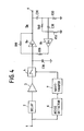
- a second embodiment of the present invention is illustrated in Fig. 4.
- the second embodiment includes a dual funcition amplifier 5a which comprises a noninverting amplifier 8a having a gain G, a feedback resistor R10 coupled fom the output to the input of amplifier 8a.
- the output of amplifier 8b is connected by a resistor R20 to the input of amplifier 8a to which is also connected one end of a capacitor C10 which is grounded at the other end.
- the junction between capacitor C30 and the input of amplifier 8b is coupled to ground by a resistor R50.
- the amplifier 8a acts as a linear amplifier due to the low output impedance of amplifier 3 as in the tirst embodiment, providing amplification of the audio signal.
- the dual function amplifier circuit 5a is represented hy an equivalent circuit shown in Fig. 5.
- Equation 15 the voltage Vo(s)
- Equation 16 By substituting Equations 16, 17 and 18 for e 10 , e 20 and e 30 of Equation 15 and providing an inverse Laplace transformation, the following Equation is obtained:
- the dual function amplifier circuit 5a has the first and second order differentiating capabilities as in the previous embodiment.
Landscapes
- Amplifiers (AREA)
- Noise Elimination (AREA)
Abstract
Description
- The present invention is related to the following copending United States Patent Applications:
- 1) Serial number 516,242, filed July 21, 1983,.by Ishigaki et al, titled "circuit for Reconstructing Noise-Affected Signals";
- 2) Serial number 517,985, filed July 29, 1983, by Y. Ishigaki, titled "Circuit Arrangement for Reconstructing Noise-Affected Signals";
- 3) Serial number 585,925, filed March 2, 1983, by Y, Ishigaki et al, titled "Impulse noise reduction by linear inerpolation having a deemphasis characteristic"; and
- 4) Serial number 585,926, filed March 2, 1984, by Y. Ishigaki et al, titled "Noise reduction by linear interpolation having immunity to white noise".
- All of the copending applications are assigned to the same assignee as the present invention.
- The present invention relates to a noise reduction circuit of the type wherein the noise-affected portion of an information signal is linearly interpolated.
- Linear interpolation techniques are known in the art as a means for reconstructing the portion of audio signals which is disrupted by a noise impulse. As shown and described in the above listed copending U.S. applications, the linear interpolation approach involves the use of two sample-and-hold circuits. The first sample-and-hold circuit is connected in a circuit between input and output terminals for generating a voltage which follows the waveform of the input signal during tracking modes and samples a voltage that occurs immediately prior to the detection of a noise impulse. During a sampling mode in which the information signal is affected by a noise impulse, the second sample-and-hold circuit generates a voltage that represents the rate with which previous gradient is expected to continue during this period and compensates for the voltage stored on the first sample-and-hold circuit.
- An object of the present invention is to simplify.the configuration of a noise reduction circuit by eliminating the second sample-and-hold circuit.
- The noise reduction circuit of the present invention comprises a noise detector connected to an input terminal for detecting a noise impulse introduced in an information signal and generating a sampling pulse time-coincident with the portion of'the signal affected by a noise impulse. A switch is provided for passing the information signal to a node between a capacitor and a noninverting amplifier in the absence of the sampling signal and blocking the signal in response to the sampling pulse. A feedback circuit having a plurality of time constant values is connected between the output and input of the amplifier to provide primary and secondary differentiation of the output signal of the amplifier. The feedback circuit is disabled during tracking modes to enable the amplifier to provide linear amplification of the voltage developed in the capacitor and is enabled during sampling modes to differentiate the voltage that occurred immediately before the switch is turned off, the differentiated signal being applied to the input of the amplifier for linearly interporating the noise-affected portion of the signal.
- The present invention will be described in further detail with reference to the accompanying drawings, in which:
- Fig. 1 is a block diagram of a first embodiment of the present invention;
- Fig. 2 is an illustation of waveforms generated in the circuit of Fig. 1;
- Fig. 3 is an illustration of an equivalent circuit of the first embodiment;
- Fig. 4 is a block diagram of a second embodiment of the present invention; and
- Fig. 5 is an illustration of an equivalent circuit of the second embodiment.
- Referring now to Fig. 1, there is shown a first embodiment of the present invention. The noise reduction circuit shown therein comprises a series combination of a
noise detector 6 and awaveshaper 7. The noise detector produces a pulse output in response to the detection of a noise impulse introduced to an audio signal applied to aninput terminal 1. The pulse output is shaped into a shaprly defined rectangular pulse and applied as a sampling pulse to a normally closed electronic switch 4 which forms part of a sample-and-hold circuit. The audio input signal is delayed by adelay circuit 2 so that the portion of the audio signal which is affected by the noise impulse is rendered time coincident with the sampling pulse. - The delayed audio signal is passed through an
amplifier 3 and switch 4 to a dualfunction amplifier circuit 5. This amplifier circuit comprises anoninverting amplifier 8 and a feedback differentiator formed by a resistor R2 and a capacitor C3 which are series connected from the output ofamplifier 8 to the input thereof to which the output ofamplifier 3 is also applied through switch 4. -
Amplifier 3 and switch 4 form a sample-and-hold circuit with a capacitor Cl which is grounded at one end and connected at the other end to the capacitor Cl. A series combination of a resistor Rl and a capacitor C2 is connected in parallel with capacitor Cl. - Dual
function amplifier circuit 5 operates as a linear amplifier when switch 4 remains closed to deliver an amplified audio signal to anoutput terminal 9 and as a slope detector when this switch is open to generate a linearly varying voltage for interpolating the noise-affected portion of the input signal. Thisnoninverting amplifier 8 has an input impedance much higher than the output impedance ofamplifier 3. - In the absence of a noise impulse, switch 4 remains in a closed circuit condition, coupling the input signal to the capacitor Cl. Since the output impedance of
amplifier 3 is much lower than the input impedance ofamplifier 8, the feedback differentiator ceases to function or disabled during the closed circuit condition with the result that capacitor Cl is charged to the voltage level of the input signal. Therefore, the potential atterminal 9 follows the voltage on capacitor C2 as long as the audio signal is not affected by noise impulses and the noise reduction circuit operates in a tracking mode. - In response to the detection of a noise impulse, shown at 20 in Fig. 2, a
sampling pulse 21 is generated and switch 4 changes over to an open circuit condition. The voltage, which appeared at the moment immediately prior to the detection of the noise, is sampled and stored in capacitor Cl and amplified with a gain G. The feedback circuit is now enabled to begin differentiating the output ofamplifier 8 and the noise-affected portion of the audio signal is interpolated with a linearly varying voltage as shown at 22 in Fig. 2. During the turn-off state of switch 4, the dualfunction amplifier circuit 5 is represented by an equivalent circuit shown in Fig. 3. If impulse noise occurs on a positive or uphill slope of the information signal, the interpolating voltage increases linearly, and if it occurs on a negative or downhill slope the voltage will decrease linearly. - A mathematical analysis of the noise reduction circuit of Fig. 1 is given with reference to the equivalent circuit. The voltage output Vo(s) which appears at
terminal 9 at the instant the open circuit condition occurs is given in Laplace transform notation by Equation 1:
- where, C1 = capacitance of capacitor C1,
- C2 = capacitance of capacitor C2,
- C3 = capacitance of capacitor C3'
- R1 = resistance of resistor Rl,
- R2 = resistance of resistor R2,
- R3 = resistance of resistor R3,
- T1 = time constant R2 x C3'
- T2 = time constant R1 x C2, and e10, e20 and e30 are voltages developed at the moment immediately prior to the detection of a noise impulse in capacitors Cl, C2 and C3, respectively. If the following relations exist:


Equation 1 can be rewritten as follows:
- Assuming that the initial voltage level at the
input terminal 1 just prior to the turn-off of switch 4 is A sin ωt, the voltages e10, e20 and e30 are respectively given by:


- By substituting
Equations 
Equation 8 can be rewritten as follows:
- Since
Equation 9 corresponds to a Tailor's series whose value at time tl and thereafter is given by
terminal 9 varies at a rate which is proportional to the first and second order differentiations of the voltage sampled at the instant immediately prior to the turn-off of switch 4. It is seen that for a noise impulse that exists for a sufficiently small duration in relation to the information signal the noise reduction circuit provides linear interpolation as shown at.22 in Fig. 2 during the noise-affected portion in which the previous gradient is expected to continue. - A second embodiment of the present invention is illustrated in Fig. 4. The second embodiment includes a
dual funcition amplifier 5a which comprises anoninverting amplifier 8a having a gain G, a feedback resistor R10 coupled fom the output to the input ofamplifier 8a. Connected between the output ofamplifier 8a and ground is a series time constant circuit including a capacitor C20 and a resistor R30 with a time constant value T 10 (= C20·R30). The junction between capacitor C20 and resistor R30 is connected to the input of a secondnoninverting amplifier 8b by a parallel time constant circuit formed by a capacitor C30 and a resistor R40 with a time constant value T20 (= C30·R40). The output ofamplifier 8b is connected by a resistor R20 to the input ofamplifier 8a to which is also connected one end of a capacitor C10 which is grounded at the other end. The junction between capacitor C30 and the input ofamplifier 8b is coupled to ground by a resistor R50. - With switch 4 being in a closed state, the
amplifier 8a acts as a linear amplifier due to the low output impedance ofamplifier 3 as in the tirst embodiment, providing amplification of the audio signal. With switch 4 being turned off, the dualfunction amplifier circuit 5a is represented hy an equivalent circuit shown in Fig. 5. - A Laplace transform notation of the output voltage Vo(s) is given by the following Equation:

amplifier 8b, - T30 = a time constant value C30(R40//R50),
- T40 = a time constant value C10(R20/R10),
- n = a constant R50/(R40 + R50), and
- By establishing the following relations,


- Assuming that the input signal at the moment immediately prior to the turn-off of switch 4 is A sin wt as in the previous embodiment, the voltages e10, e20 and e30 developed in capacitors C10, C20 and C30 at the same moment for angular frequencies ω much lower than 2π/T10 and 2π/T20 are given by the following Equations:


- Vo(t) = G·A{sin ωt1 + (t - t1)ω.sin(ωt1 + 90) +

- From Equation 19 it is seen that the dual
function amplifier circuit 5a has the first and second order differentiating capabilities as in the previous embodiment.
Claims (6)
Applications Claiming Priority (2)
| Application Number | Priority Date | Filing Date | Title |
|---|---|---|---|
| JP58144651A JPS6035838A (en) | 1983-08-08 | 1983-08-08 | Reducing device of impulsive noise |
| JP144651/83 | 1983-08-08 |
Publications (3)
| Publication Number | Publication Date |
|---|---|
| EP0136482A2 true EP0136482A2 (en) | 1985-04-10 |
| EP0136482A3 EP0136482A3 (en) | 1986-04-09 |
| EP0136482B1 EP0136482B1 (en) | 1989-05-03 |
Family
ID=15367035
Family Applications (1)
| Application Number | Title | Priority Date | Filing Date |
|---|---|---|---|
| EP84109445A Expired EP0136482B1 (en) | 1983-08-08 | 1984-08-08 | Noise reduction by linear interpolation using a dual function amplifier circuit |
Country Status (4)
| Country | Link |
|---|---|
| US (1) | US4577161A (en) |
| EP (1) | EP0136482B1 (en) |
| JP (1) | JPS6035838A (en) |
| DE (1) | DE3478078D1 (en) |
Cited By (1)
| Publication number | Priority date | Publication date | Assignee | Title |
|---|---|---|---|---|
| GB2472992A (en) * | 2009-08-25 | 2011-03-02 | Zarlink Semiconductor Inc | Reduction of clicking sounds in audio data streams |
Families Citing this family (10)
| Publication number | Priority date | Publication date | Assignee | Title |
|---|---|---|---|---|
| JPS62132434A (en) * | 1985-12-05 | 1987-06-15 | Clarion Co Ltd | Gate circuit |
| GB8706962D0 (en) * | 1987-03-24 | 1987-04-29 | Filtronic Components Ltd | Oscillator |
| JP2570485B2 (en) * | 1990-09-19 | 1997-01-08 | 日本ビクター株式会社 | Signal interpolation circuit |
| DE69221434T2 (en) * | 1991-11-15 | 1997-12-11 | Asahi Glass Co Ltd | Image display device and method for controlling the same |
| IT1272418B (en) | 1993-04-29 | 1997-06-23 | Alcatel Italia | SYSTEM FOR THE TREATMENT OF SIGNALS AFFECTED BY TRANSMISSION ERRORS |
| KR0182943B1 (en) * | 1995-02-04 | 1999-04-15 | 김광호 | Noise filtering circuit for audio signal |
| US5859392A (en) * | 1996-02-09 | 1999-01-12 | Lsi Logic Corporation | Method and apparatus for reducing noise in an electrostatic digitizing tablet |
| IT1308062B1 (en) * | 1999-05-28 | 2001-11-29 | St Microelectronics Srl | PROTECTION CIRCUIT TO REDUCE NOISE ON DENSITY REFERENCES, IN PARTICULAR IN DC-DC CONVERTERS |
| DE102004025300A1 (en) * | 2004-05-19 | 2005-12-15 | Micronas Gmbh | Device and method for noise suppression |
| US7724042B2 (en) * | 2007-07-06 | 2010-05-25 | Texas Instruments Incorporated | Reducing power consumption in an amplification stage driving a sample and hold circuit while maintaining linearity |
Citations (4)
| Publication number | Priority date | Publication date | Assignee | Title |
|---|---|---|---|---|
| US4076969A (en) * | 1975-04-07 | 1978-02-28 | Singer & Singer | Impulse noise reduction system |
| DE2929030A1 (en) * | 1978-07-18 | 1980-02-07 | Matsushita Electric Ind Co Ltd | PROCESS FOR INTERRUPTION OF INTERFERENCE |
| EP0099760A2 (en) * | 1982-07-21 | 1984-02-01 | Victor Company Of Japan, Limited | Circuit for reconstructing noise-affected signals |
| EP0103385A2 (en) * | 1982-07-30 | 1984-03-21 | Victor Company Of Japan, Limited | Circuit arrangement for reconstructing noise-affected signals |
Family Cites Families (1)
| Publication number | Priority date | Publication date | Assignee | Title |
|---|---|---|---|---|
| DE2262560A1 (en) * | 1972-12-21 | 1974-06-27 | Blaupunkt Werke Gmbh | METHOD AND DEVICE FOR SUPPRESSING MALFUNCTIONS IN AN ELECTRICAL SIGNAL |
-
1983
- 1983-08-08 JP JP58144651A patent/JPS6035838A/en active Granted
-
1984
- 1984-08-08 DE DE8484109445T patent/DE3478078D1/en not_active Expired
- 1984-08-08 EP EP84109445A patent/EP0136482B1/en not_active Expired
- 1984-08-08 US US06/638,779 patent/US4577161A/en not_active Expired - Lifetime
Patent Citations (4)
| Publication number | Priority date | Publication date | Assignee | Title |
|---|---|---|---|---|
| US4076969A (en) * | 1975-04-07 | 1978-02-28 | Singer & Singer | Impulse noise reduction system |
| DE2929030A1 (en) * | 1978-07-18 | 1980-02-07 | Matsushita Electric Ind Co Ltd | PROCESS FOR INTERRUPTION OF INTERFERENCE |
| EP0099760A2 (en) * | 1982-07-21 | 1984-02-01 | Victor Company Of Japan, Limited | Circuit for reconstructing noise-affected signals |
| EP0103385A2 (en) * | 1982-07-30 | 1984-03-21 | Victor Company Of Japan, Limited | Circuit arrangement for reconstructing noise-affected signals |
Cited By (2)
| Publication number | Priority date | Publication date | Assignee | Title |
|---|---|---|---|---|
| GB2472992A (en) * | 2009-08-25 | 2011-03-02 | Zarlink Semiconductor Inc | Reduction of clicking sounds in audio data streams |
| US8311229B2 (en) | 2009-08-25 | 2012-11-13 | Microsemi Semiconductor Corp. | Reduction of clicking sounds in audio data stream |
Also Published As
| Publication number | Publication date |
|---|---|
| US4577161A (en) | 1986-03-18 |
| JPS6325543B2 (en) | 1988-05-25 |
| EP0136482A3 (en) | 1986-04-09 |
| DE3478078D1 (en) | 1989-06-08 |
| EP0136482B1 (en) | 1989-05-03 |
| JPS6035838A (en) | 1985-02-23 |
Similar Documents
| Publication | Publication Date | Title |
|---|---|---|
| EP0135081B1 (en) | Noise reduction by linear interpolation using a dual function amplifier circuit | |
| US3636463A (en) | Method of and means for gainranging amplification | |
| EP0136482A2 (en) | Noise reduction by linear interpolation using a dual function amplifier circuit | |
| US4204170A (en) | Impulse noise limiter circuit | |
| US4112381A (en) | Peak detector | |
| EP0135039A1 (en) | Noise reduction by linear interpolation using a single sample-and-hold circuit | |
| US2856468A (en) | Negative feedback amplifier in a measuring system | |
| US3054064A (en) | D.-c. output frequency discriminators using lag lead phase shift networks, sampling, and averaging circuits | |
| US3479599A (en) | Signal sensitive depressed threshold detector | |
| US3036224A (en) | Limiter employing operational amplifier having nonlinear feedback circuit | |
| US4531095A (en) | Impulse noise reduction by linear interpolation having immunity to white noise | |
| GB1563873A (en) | Noise clearing system | |
| US4247823A (en) | Low noise, low phase shift analog signal multiplier | |
| US3287695A (en) | Self-adjusting inverse filter | |
| US4532475A (en) | Impulse noise reduction by linear interpolation having a deemphasis characteristic | |
| US3488597A (en) | Pulse averaging circuit | |
| US3461406A (en) | Delta modulator using operational integration | |
| JPS58111417A (en) | Amplitude controller | |
| US2776369A (en) | Video integrator circuits | |
| US3497805A (en) | Circuit including a constant amplitude pulse generator for adjusting the amplitude of pulses produced by a transducer | |
| US3363189A (en) | Synchronous demodulator | |
| US3096448A (en) | Pulse sampling device employing modulated multivibrator to slice leading and trailing edges of input | |
| SU809522A1 (en) | Shaper for referencing pulses | |
| US4434404A (en) | A.C. Coupled video amplifier with fast pulse recovery | |
| SU1256188A1 (en) | Pulse-width modulator |
Legal Events
| Date | Code | Title | Description |
|---|---|---|---|
| PUAI | Public reference made under article 153(3) epc to a published international application that has entered the european phase |
Free format text: ORIGINAL CODE: 0009012 |
|
| AK | Designated contracting states |
Designated state(s): DE FR GB |
|
| PUAL | Search report despatched |
Free format text: ORIGINAL CODE: 0009013 |
|
| AK | Designated contracting states |
Kind code of ref document: A3 Designated state(s): DE FR GB |
|
| 17P | Request for examination filed |
Effective date: 19860521 |
|
| 17Q | First examination report despatched |
Effective date: 19880204 |
|
| GRAA | (expected) grant |
Free format text: ORIGINAL CODE: 0009210 |
|
| AK | Designated contracting states |
Kind code of ref document: B1 Designated state(s): DE FR GB |
|
| REF | Corresponds to: |
Ref document number: 3478078 Country of ref document: DE Date of ref document: 19890608 |
|
| ET | Fr: translation filed | ||
| PLBE | No opposition filed within time limit |
Free format text: ORIGINAL CODE: 0009261 |
|
| STAA | Information on the status of an ep patent application or granted ep patent |
Free format text: STATUS: NO OPPOSITION FILED WITHIN TIME LIMIT |
|
| 26N | No opposition filed | ||
| PGFP | Annual fee paid to national office [announced via postgrant information from national office to epo] |
Ref country code: DE Payment date: 20010730 Year of fee payment: 18 |
|
| PGFP | Annual fee paid to national office [announced via postgrant information from national office to epo] |
Ref country code: GB Payment date: 20010808 Year of fee payment: 18 |
|
| PGFP | Annual fee paid to national office [announced via postgrant information from national office to epo] |
Ref country code: FR Payment date: 20010810 Year of fee payment: 18 |
|
| REG | Reference to a national code |
Ref country code: GB Ref legal event code: IF02 |
|
| PG25 | Lapsed in a contracting state [announced via postgrant information from national office to epo] |
Ref country code: GB Free format text: LAPSE BECAUSE OF NON-PAYMENT OF DUE FEES Effective date: 20020808 |
|
| PG25 | Lapsed in a contracting state [announced via postgrant information from national office to epo] |
Ref country code: DE Free format text: LAPSE BECAUSE OF NON-PAYMENT OF DUE FEES Effective date: 20030301 |
|
| GBPC | Gb: european patent ceased through non-payment of renewal fee |
Effective date: 20020808 |
|
| PG25 | Lapsed in a contracting state [announced via postgrant information from national office to epo] |
Ref country code: FR Free format text: LAPSE BECAUSE OF NON-PAYMENT OF DUE FEES Effective date: 20030430 |
|
| REG | Reference to a national code |
Ref country code: FR Ref legal event code: ST |